THE AMPLIPHASE TRANSMITTER --AN INVESTIGATION
Apart from the original paper* I have not found a rigorous treatment of Ampliphasse transmitters.
This section of my web site is an attempt to correct this.
It is an open invitation to anyone who has either designed or operated an Ampliphase transmitter to contribute or critisise.
The fourth section of the site contains numerical solutions and rigorous algebraic analysis of the circuitry used in
Ampliphase or Outphasing transmitters.
It is now fairly complete and can be used as a reference in any discussion.
The first and second sections on models and transmitters will be added to as time and received information permits.
*HIGH POWER OUTPHASING MODULATION
by
H. CHIREIX
Proc. IRE November 1935
CONTACT : COMMENTS AND QUESTIONS
back/home
As the name of this Website would suggest, I have had an interest in high fidelity AM tramission on
the broadcast band since mid last century.
The usual transmitter topology using high level modulation with choke coupling from a class B amplifier
exceeded the limitations of most receivers.
There was little incentive for any broadcaster to change this to cater for a very small minority with high
performance tuners.
This is discussed more fully in the "HISTORY" section.
The quest for lower distortion - though of minority interest - then led to the consideration of
alternative topologies.
The abandonment of:-
[1] Class B amplifiers with their accompanying crossover distortion.
[2] All ironmongery - output transformers and coupling chokes.
These produce distortion at low frequencies due to the non-linear B-H magnetising curve and a high
frequency transfer function destabilising to overall envelope feedback due to winding capacity
and leakage inductance.
These considerations dictate LOW LEVEL MODULATION
A transmitter with low level grid modulation followed by class B "linerar" amplifiers with a high degree of
overall envelope feedback can produce high quality AM, but is ruled out because of low efficiency.
In the fifties there seemed to be only two choices left:-
[A] Low level modulation followed by Doherty high efficiency RF amplifiers.
[B] Ampliphase or Outphasing.
The Doherty amplifier employs a separate high level output stage which switches on as the carrier increases
for positive modulation.
This produces a discontinuity in the transfer characteristic equivalent to cross over distortion in
the class B amplifier.
The Ampliphase Transmitter seemed the most likely candidtate for study.
In the Ampliphase transmitter two carriers are phase modulated in opposite directions at a low power level.
The power level of these two signals is increased in identical high efficiency saturated stages - saturated because,
ideally, there is no amplitude modulation on the signal.
It is not until the signals are added algebraically in the antenna circuit that AM appears.
Phase modulation tends to throw up non-linear equations governing the dynamic response.
These non-linear equations can only be solved by numerical methods - tedious and not practible with the
low computer speed in the mid fifties.
Experimental methods using model transmitters at the 10 watt power level were the solution
Because the work was done in isolation, many of the ideas were different from those in the RCA transmitters.
A description of them will be included as time permits.
The previously missing numerical solutions are now included in section four.
The original paper by Chireix was not available in the fifties when this work was done.
It is interestting to reflect that Chireix had the same thoughts, but was at least thirty years ahead.
Chireix on high and low level modulation:-
And Chireix again on the properties of high and low level modulation.:-
The introduction of phase modulation to secure AM was a by-product of a more fundamental consideration in
Chireix's original paper :-
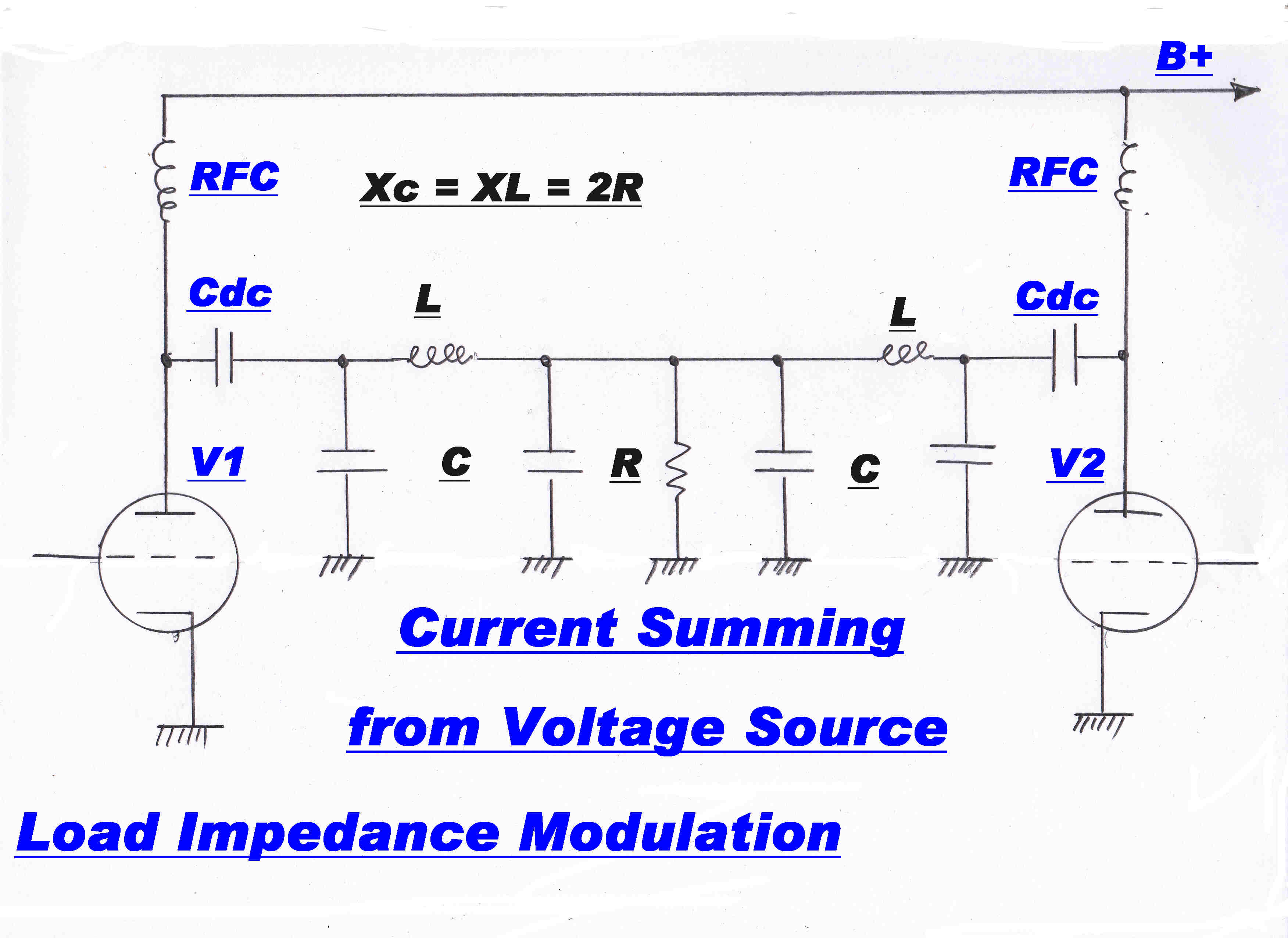
LOAD IMPEDANCE MODULATION
And again from the original paper :-
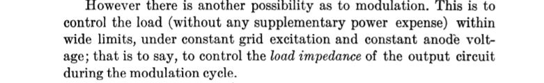
There are a number of methods to modulate the load impedance - mechanical : with the variable
resistance of a carbon microphone (Fessenden) or the variation of the coupling to the load
with a variable saturable reactor as suggested by Chireix :-
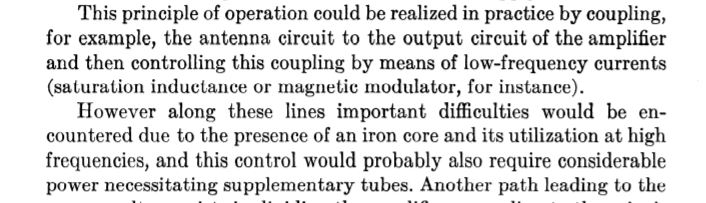
 Load Impedance Modulation was not a new idea.
In fact, it was used by Fessenden in the first great broadcast from Brant Rock on Xmas Eve 1906:-
The circuit shown on the right is a good representation of the system Fessenden used to produce
load impedance modulation of the sinusoidal carrier produced by his high speed variable reluctance alternator.
Lg CTa LTa form a series tuned circuit resonant at carrier frequency.
The output current from the alternator is determined by the total series resistance:-
[A] The alternator output resistance
[B] + The resistance reflected from the antenna through M
[C] + The resistance of the carbon microphone - water cooled because it was subjected to the full transmitter power.
Variation of the resistance of the carbon microphone by audio would vary the resistance and so produce AM.
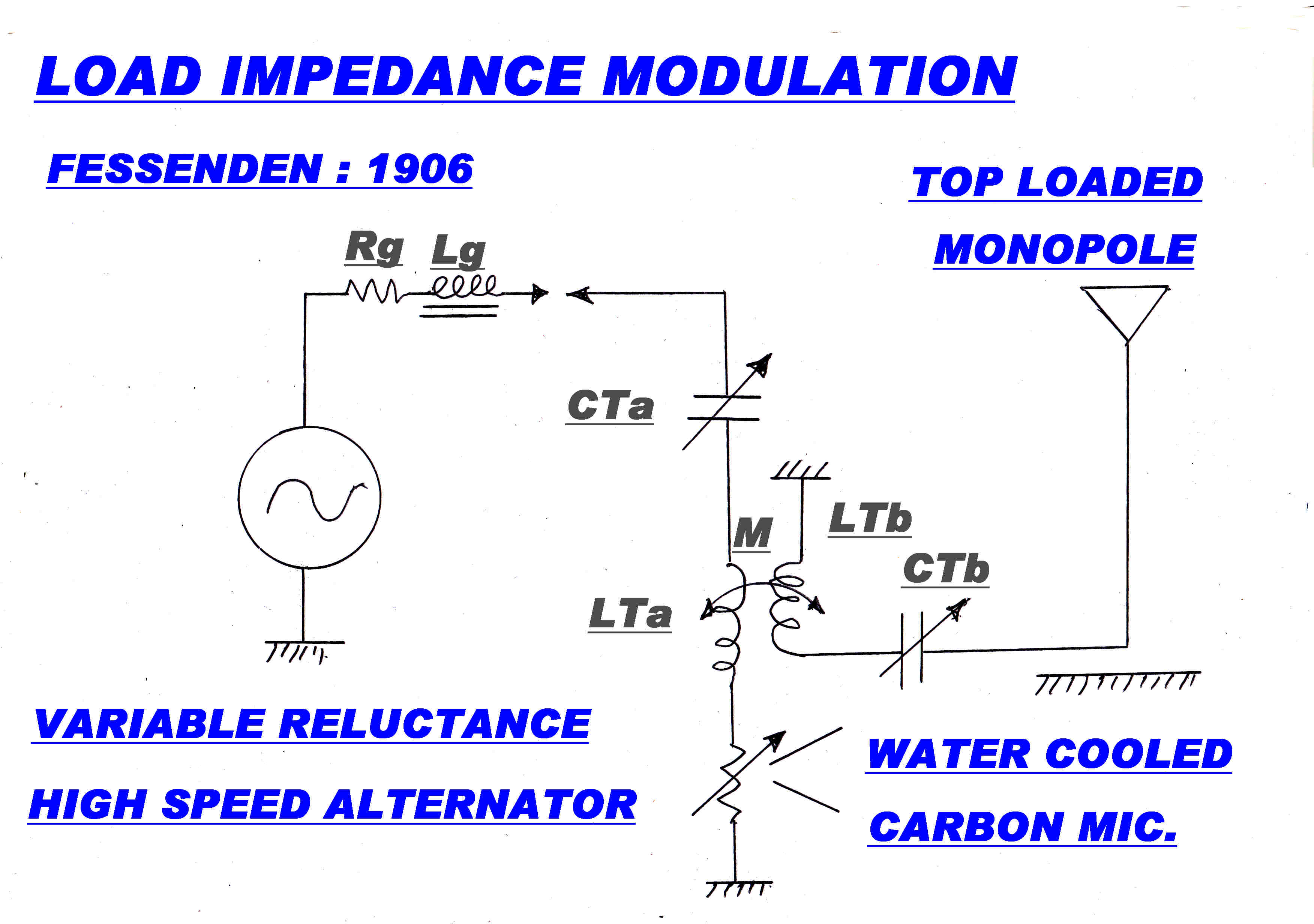
 Although not directly connected to Ampliphase transmitters, a few words on
Fessenden's variable reluctance alternator.
Although not directly connected to Ampliphase transmitters, a few words on
Fessenden's variable reluctance alternator.
The basic idea is important.
It was used in the design of audio equipment - for exmple the WE4A pickup described in another section
of this site.
The trick is to minimise the amount of iron used in magnetic circuits operating at high frequencies where the
losses are high.
The total magbetic flux is held constant in the main magnetic circuit so there are no AC losses.
The flux is then diverted from one short path in laminated iron to another with a high permeability blade
to produce flux variation and so output voltage.
The carrier alternators operated up to frequency of 100KHz.
It is believed Fessenden's broadcast was on 88KHz - the carrier frequency stability depending on the
constanccy of the speed of the driving DC motor.
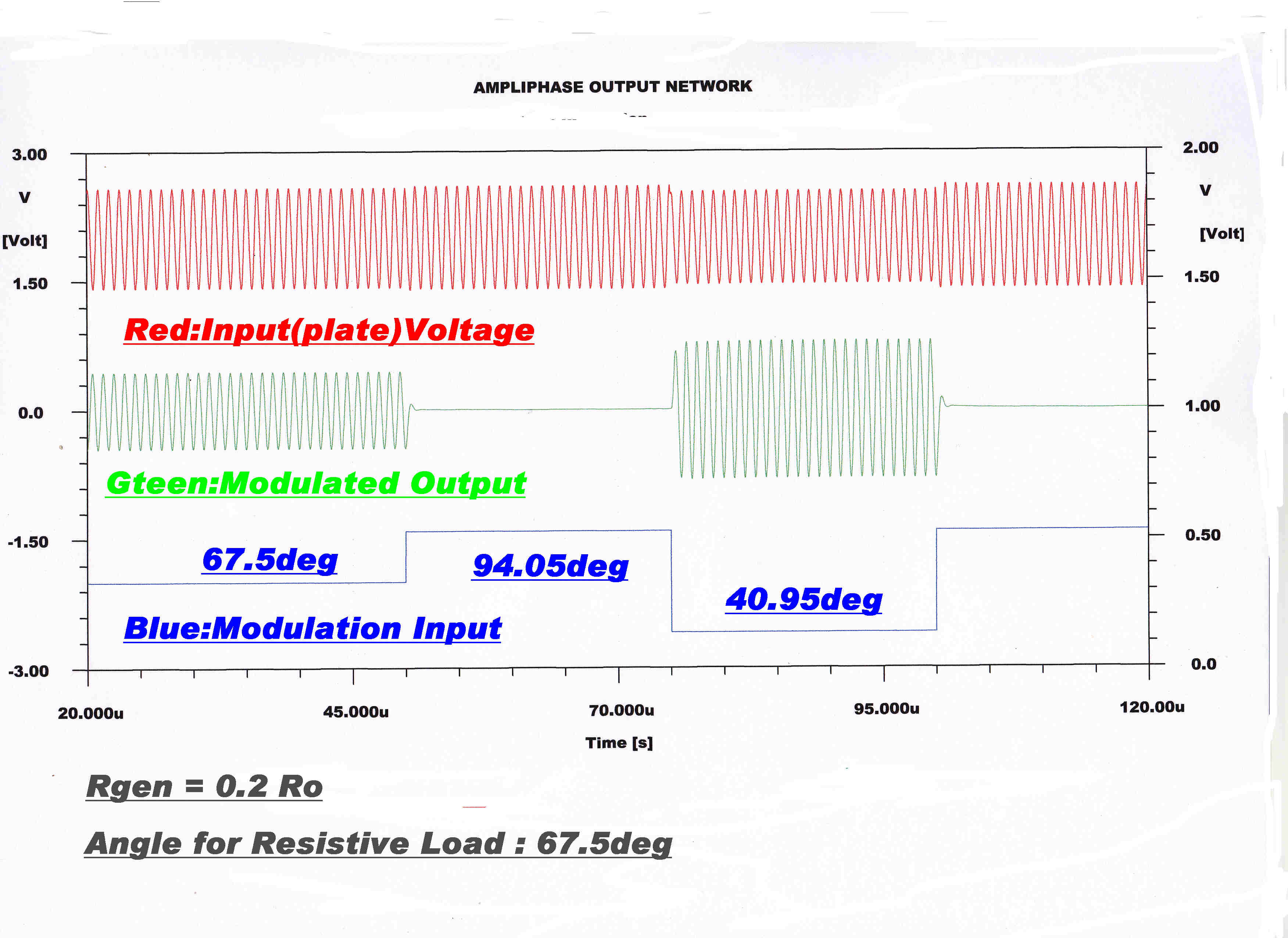
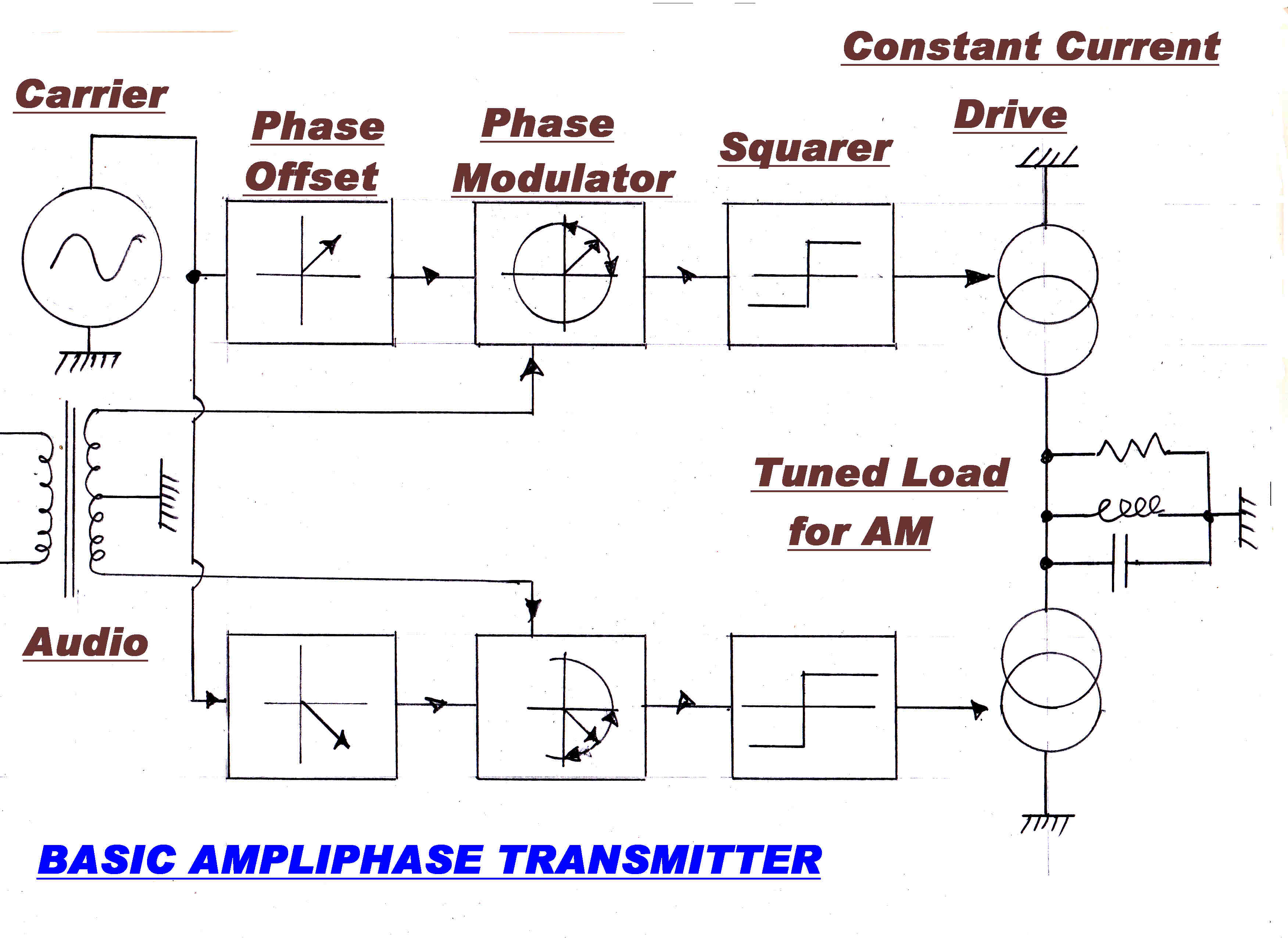 The block diagram of a simple Ampliphase transmitter is shown on the right.
A low level sine wave at carrier frequency drives two identical channels.
In the upper channel there is a phase offset of +45 degrees and in the
lower channel -45 degrees.
Push-pull audio is applied to linear phase modulators to give a phase deviation of
+(-) 45 degrees on one channel and -(+) 45 degrees on the other.
At one limit the outputs will be in phase and at the other 180 degrees out of phase.
Many phase modulators also produce incidental amplitude modulation.
This is removed by a limiter or slicer.
The two phase modulated waves are then added algebraically to produce AM
with no residual phase modulation because of the symmetry.
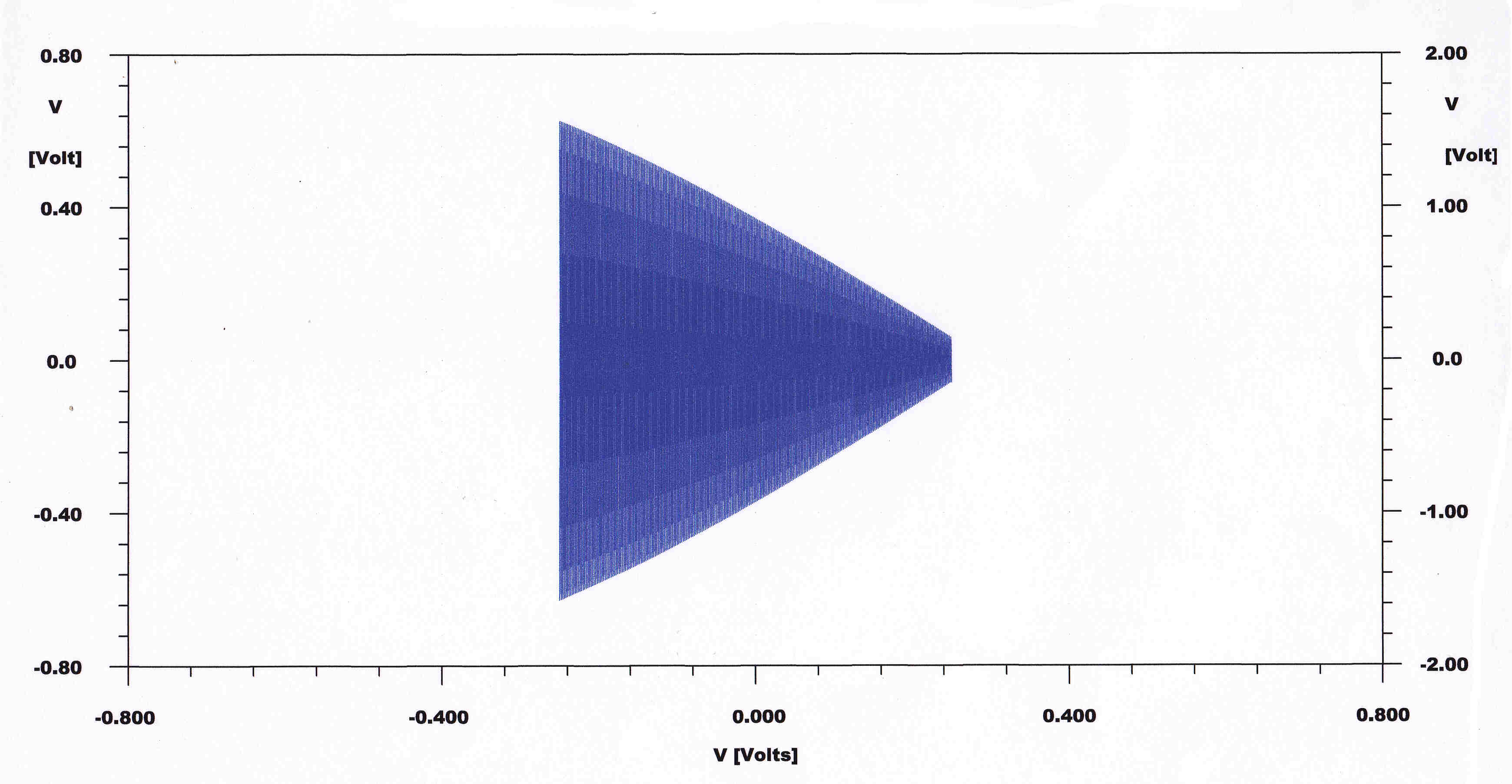
We can now evaluate the transfer characteristic of the simple transmitter.
The output current from one side will be I sin( ω t + φ )
and on the other I sin( ω t - φ ) .
The total output current I(t) will be:-
I(t) = I [ sin( ω t + φ ) + sin( ω t - φ ) ]
= I [ cos(φ) ] sin( ω t )
The transfer characteristic is [ cos(φ) ] which gives the trapezoidal patttern
shown on the right.
The gross non-linearity would result in horrendous distortion.
Three techniques are used to to improve the linearity:-
[1] Use only the more linear part of the curve.
[2] Pre-distort the phase modulation to be the inverse of the cosine curve.
[3] Amplitude modulate the current I with an error correcting voltage.
In the RCA Ampliphase transmitters the techniques in [1] and [3] were used.
[1] The initial offset was 67.5 degrees with linear phase modulation of +(-) 22.5 degrees
to give a (half) phase change from 90 degrees (zero carrier) to 45 degrees ( peak carrier ).
[2] The driver (one stage before the output stage ) was grid modulated to produce corrective AM in the
the grid drive to the final stage.
The non-linear correction signal was produced by distorting the audio in an amplifier
with a tube (6AG7) which turns on only for a part of the cycle giving a break point equivalent
to crossover distortion.
Note that the ideal of saturation in the RF stages has been lost.
They are now required to pass signals with AM.
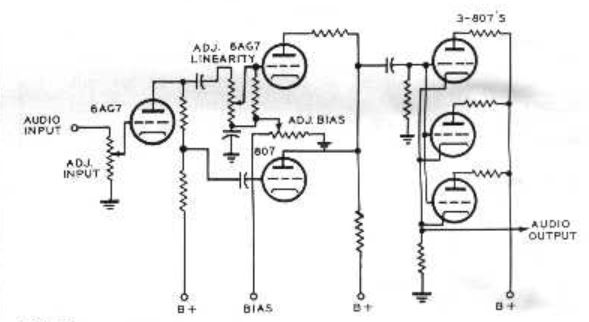 An outline of the circuit to produce the non-linear signal for grid modulation
of the driver stage was published br RCA.
An outline of the circuit to produce the non-linear signal for grid modulation
of the driver stage was published br RCA.
It is shown on the right.
It is rather optimistically called the "linearity" stage : perhaps a better and
more acccurate name would be the "NON-linearity" stage.
Note that there are three interacting preset controls - a test for the temper and
well being of any poor soul who encountered them!
 We can produce phase modulation by taking a suppressed carrier AM wave
Va m(t) sin( ωct + β ) modulated by m(t) and adding it
an out of phase sine wave of constant amplitude Vc sin( ωct + α ) then :-
We can produce phase modulation by taking a suppressed carrier AM wave
Va m(t) sin( ωct + β ) modulated by m(t) and adding it
an out of phase sine wave of constant amplitude Vc sin( ωct + α ) then :-
V(t) = Vc sin( ωct + α ) + Va m(t) sin( ωct + β )
Some algebra results in :-
V(t) = [ sin( ωt )][ Vc cos(α) + Va m(t) cos(β) ]
+ [ cos( ωt ) ][ Vc sin(α) - Va m(t) sin(β ) ]
If the phase angle of V(t) is φ then :-
tan(φ) = [ sin(α) - Va/Vc m(t) sin(β)]/[ cos(α) + Va/Vc m(t) cos(β) ]
If we simplify by putting:-
α = β = ζ and Va = Vc = 1 then :-
tan(φ) = tan(ζ) [ 1 - m(t) ]/[ 1 + m(t) ]
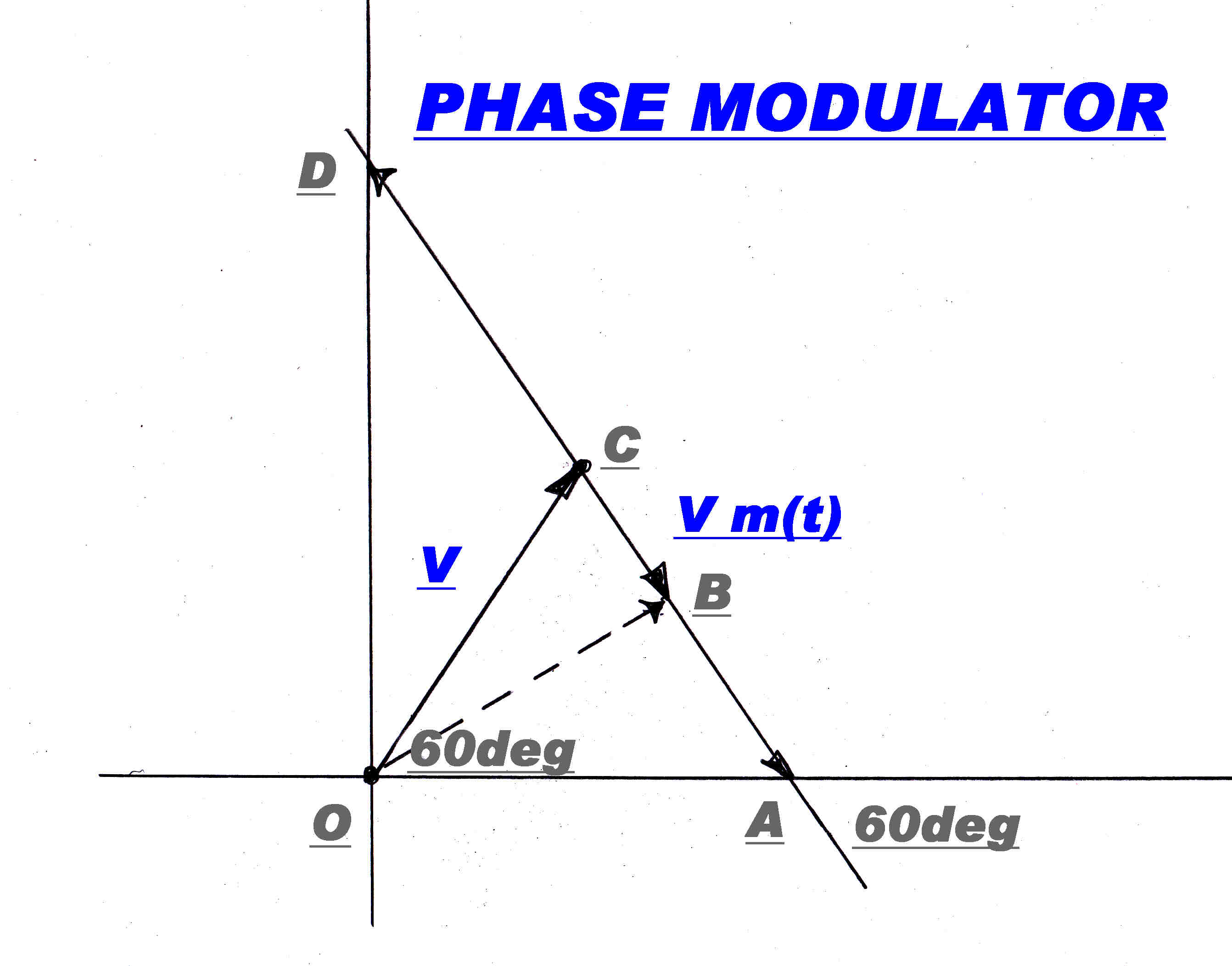
The phasor diagram for ζ = 60 degrees is shown opposite.
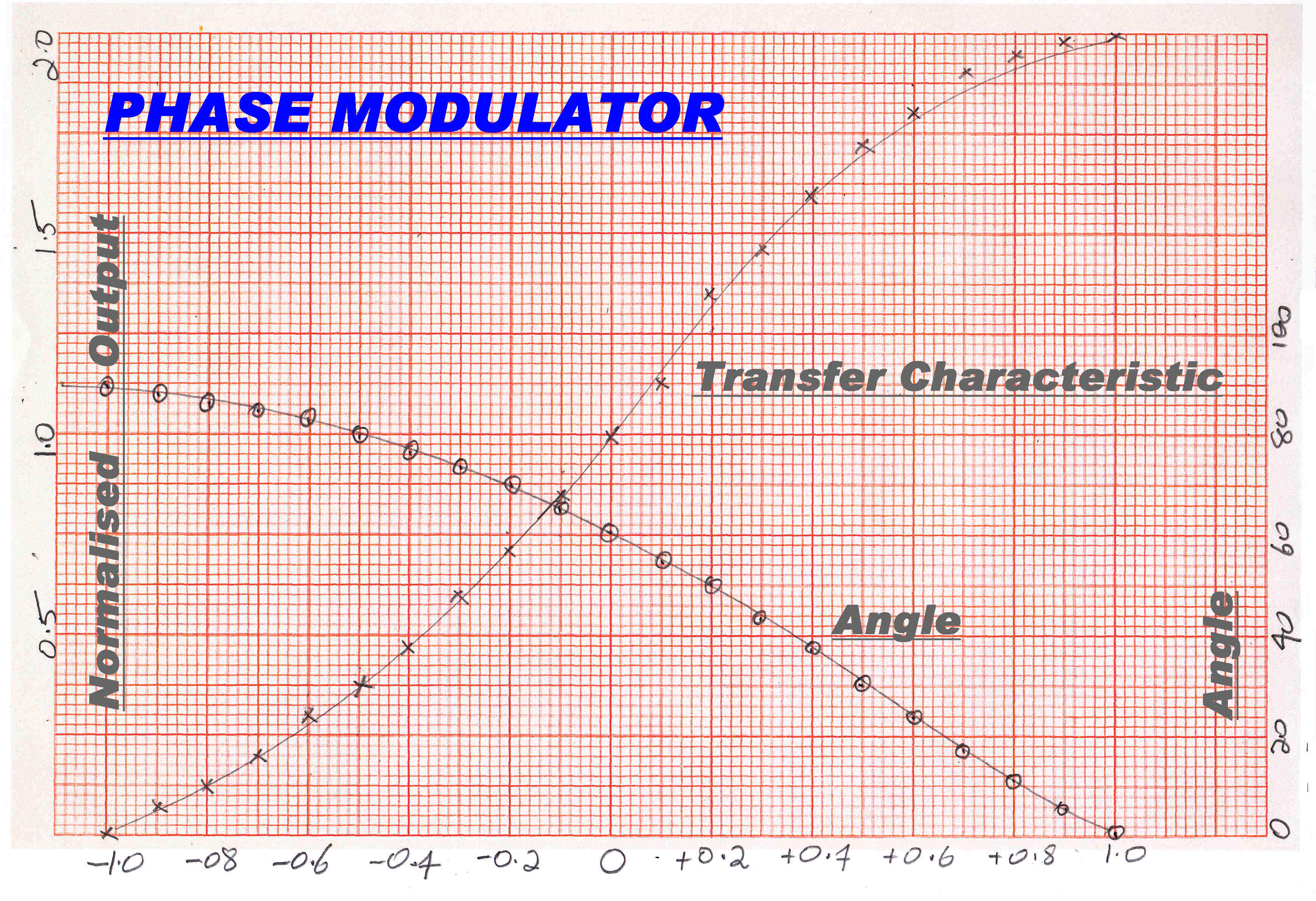
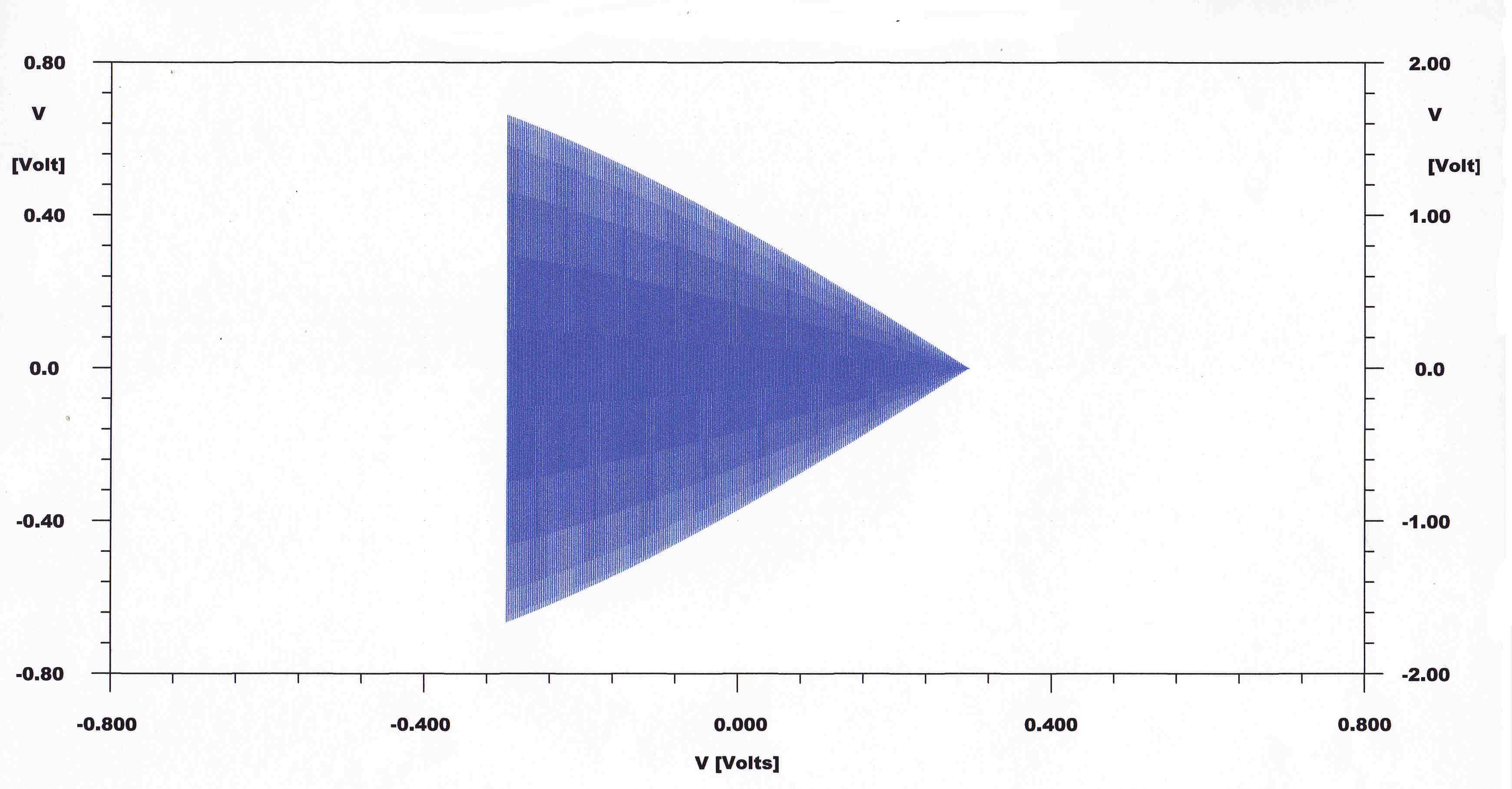
We can evaluate cos(φ) to give the transfer characteristic shown below.
Non-linearity in the phase modulator has corrected some of the non-linearity experienced
with a linear phase modulator.
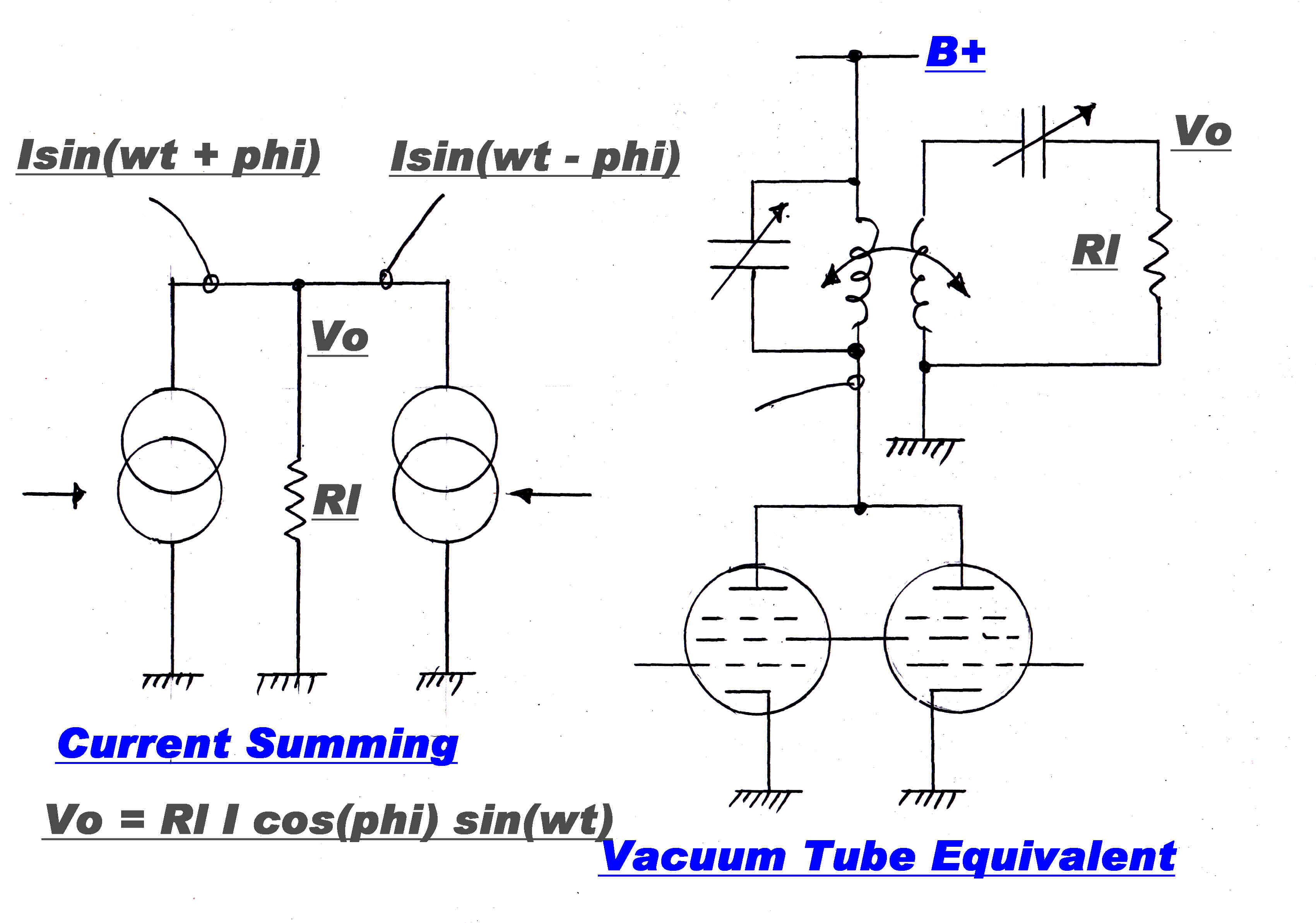
Fessenden used a carbon microphone to modulate the load on a high frequency alternator to produce AM.
The production of load modulation with vacuum tubes is not so obvious.
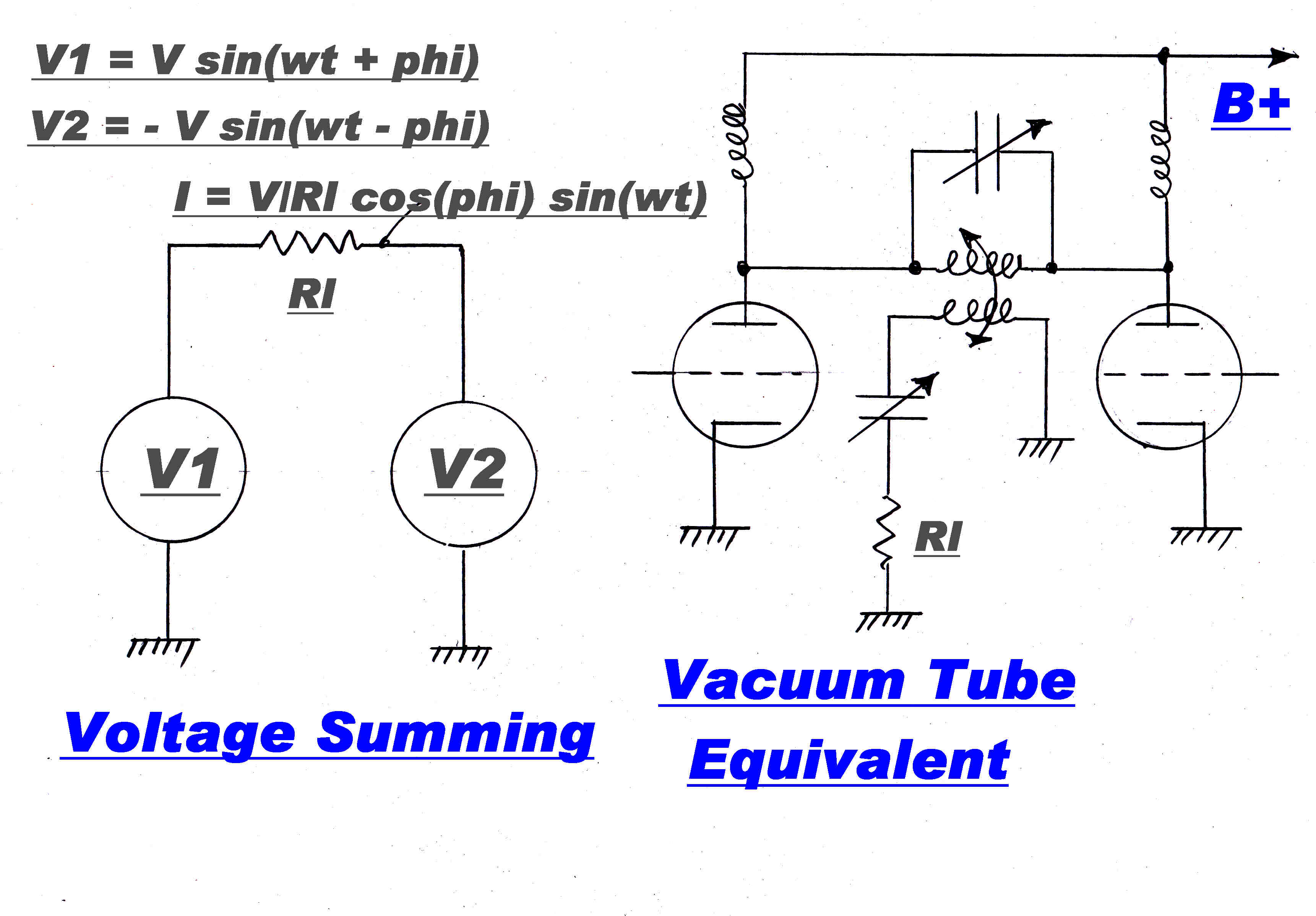
Chireix solved the problem by using two out of phase generators V1 and V2.
The output voltage Vout for the two voltage generators in series ( V1 + V2 ) will be out of phase
with either generator.
Vout = V1 + V2
If Vout is applied across a resistive load R to give a current Iout = Vout/R, then the output current will be out of phase
with the output voltage of either generator, so both generators will see a complex load modulated by the phase
difference between them.
This is the basic trick behind OUTPHASING and AMPLIPHASE transmitters.
The generators may be either voltage or current generators.
 The load current ILis given by:-
IL = I [ sin(ωt + φ ) + sin(ωt - φ ) ]
= I [ sin(ωt)cos(φ) + sin(φ)cos(ωt) +
sin(ωt)cos(φ) - sin(φ)cos(ωt) ]
vout(t) = 2 I R cos(φ) sin(ωt)
Now transferring to steady state complex notation:-
VL = 2 I R cos(φ)
IL = I [ cos(φ) + i sin(φ) ]
ZL = VL/IL
= [ 2 I R cos(φ) ]/ [ I ( cos(φ) + i sin(φ) ) ]
= 2 R cos(φ) [ cos(φ) - i sin(φ) ]/[ cos2(φ) + sin2(φ ) ]
= 2 R cos(φ) [ cos(φ) - i sin(φ) ]
So: |ZL| = 2 R cos(φ ) :: Ang: ZL = -φ
it is easy to produce a constant current generator with vacuum tubes - for instance a pentode with a very
high plate resistance or a triode with cathode current feedback.
The efficiency for amplitude modulated waves must be low.
At peak 100% modulation the maximum plate swing is just below the applied B+ high tension voltage.
This will give the maximum efficiency whether the tube is operated under class A, B, or C conditions.
The DC input current - and so the input power - does not change when the carrier output goes to zero, so the overall efficiency
over a modulation cycle is very low.
The configuration, then, is of no use in the output stage of a high power transmitter.
It is very useful to generate feedback in phase modulators operating at a low power level.
 The output voltage VLis given by:-
VL = V [ sin(ωt + φ ) + sin(ωt - φ ) ]
= V [ sin(ωt)cos(φ) + sin(φ)cos(ωt) +
sin(ωt)cos(φ) - sin(φ)cos(ωt) ]
Iout(t) = 2 V/Rl cos(φ) sin(ωt)
Now transferring to steady state complex notation:-
IL = 2 V/Rl cos(φ)
VL = V [ cos(φ) + i sin(φ) ]
ZL = VL/IL
= [ V ( cos(φ) + i sin(φ) ) ]/[ 2 V/Rl cos(φ) ]
= [Rl/(2 cos(φ)) ][ cos(φ) + i sin(φ) ]
= [Rl/(2 cos(φ)) ][ cos(φ) + i sin(φ) ]
So: |ZL| = Rl /(2 cos(φ ) ) :: Ang: ZL = φ
Vacuum tubes can approximate constant current generators very closely, but are a poor
approximation for voltage generators: yet the voltage generator model is the one chosen for the high
power output stage of an Ampliphase transmitter.
It is possible to obtain high efficiency with the voltage generator model.
Because the output voltage ( the RF voltage swing on the plate) is constant, a value can be taken
nearly equal to the high tension B+ voltage.
This gives the fundamental condition for high efficiency.
From the above equation, the load impedance presented to the plate of the output tube is given by:-
|ZL| = Rl /(2 cos(φ ) )
so the magnitude approaches infinity for low carrier outputs as φ → 90 degrees.
If the grid drive were kept constant, the tube would "bottom" with the RF swing on the plate increasing only slightly,
but with a great increase in grid current.
The grid drive must be reduced for large drive angles.
This requires that the drive be modulated, and so the constant drive ideal is lost.
In the RCA Ampliphase transmitter the AM drive was produced by the non-linear stage described above.
Grid modulation of the driver stage was at a low power level requiring only three 807 pentodes in parallel.
 It is shown above that the output tubes must be operated as constant voltage
generators for high efficiency.
It is shown above that the output tubes must be operated as constant voltage
generators for high efficiency.
The generators must be in series and in series with the load.
This is inconvenient - it is much easier to parallel current generators across a load.
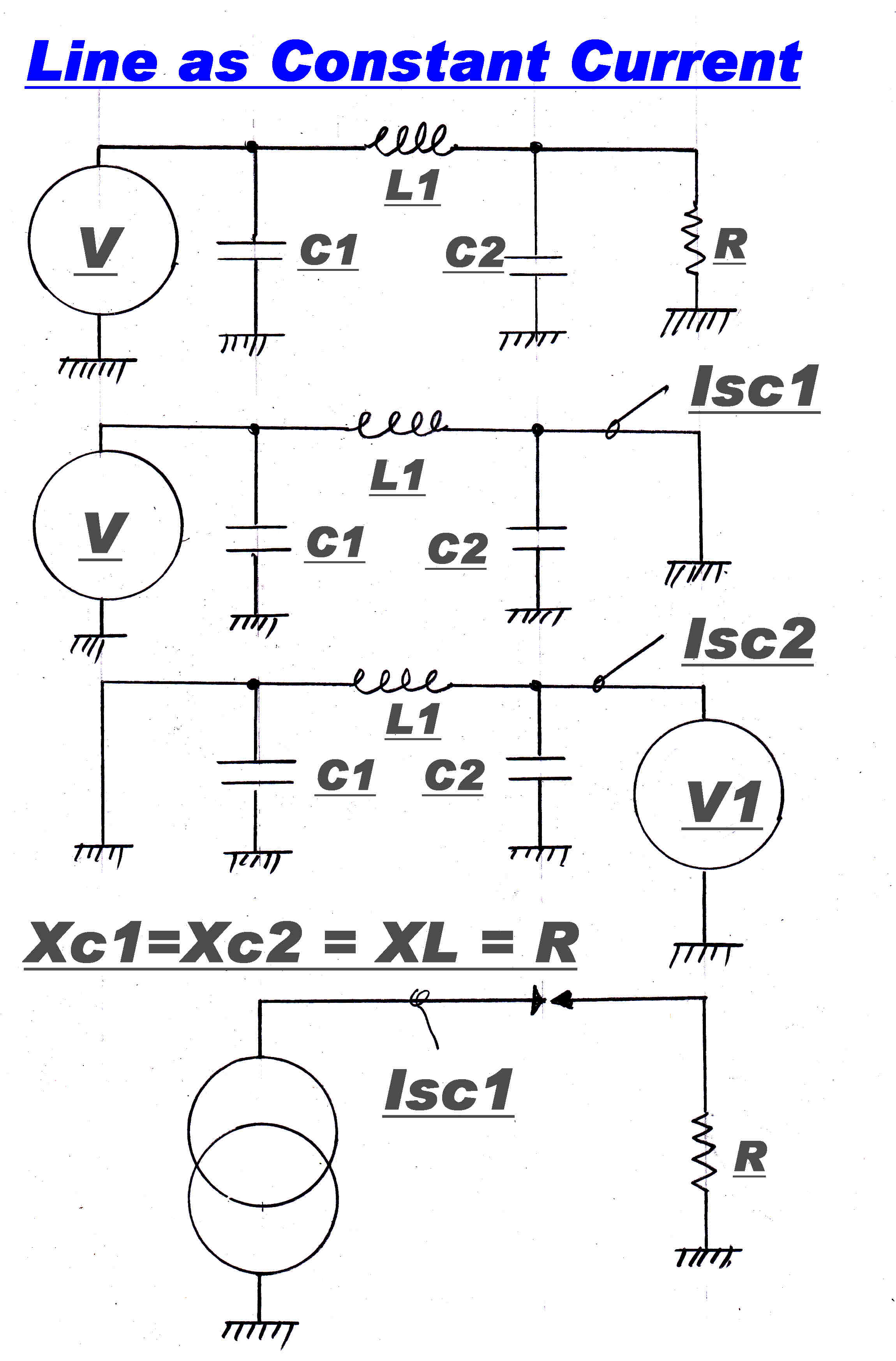
λ/4 lines convert voltage generators to current generators and so allow parallel addition across the load.
This can easily be shown by applying Thevenin:-
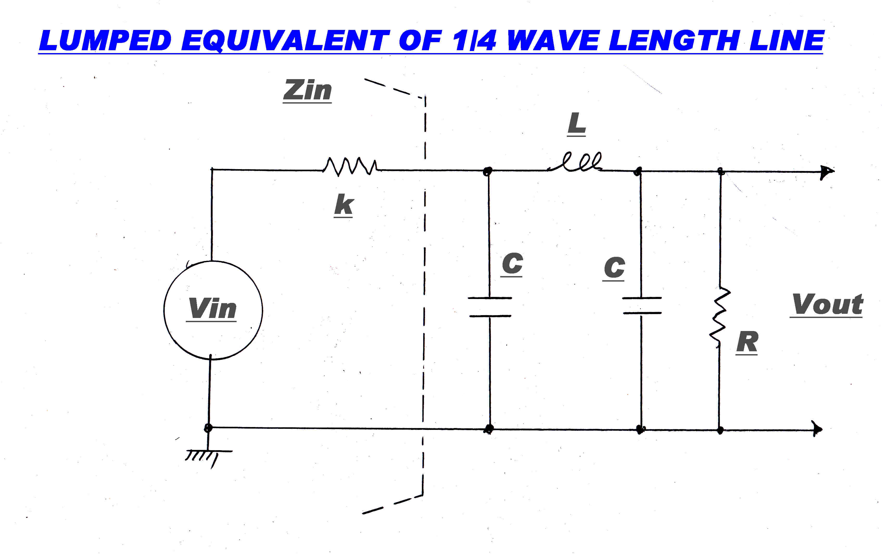
For a λ/4 lumped line we have:-
XC1 = XC2 = XL1 = R
If we short circuit the output, then the current will be:-
Isc1 = V/( i ω L1)
If we determine the output impedance by short circuiting the input and applying a test voltage generator
to the input:-
Then the input impedance is given by L1 and C2 in parallel.
These form a parallel resonant circuit with infinite impedance since:-
XC2 = XL1
The λ/4 network then turns the voltage generator into a current generator I where
I = V/( i ω L1)
There is a phase change of -90 degrees in the network.
The network also has some practical advantages:-
[1] It has capacity to earth across the voltage generator and the load, allowing easy realisation
of a practical output network.
[2] It takes the form of a low pass filter and so helps in attenuating the harmonics in a class C stage.
The λ/4 network is not fundamental to an Ampliphasae transmitter.
It simply produces a convenient output circuit.
The above analysis holds only for carrier frequency, but the transmitter must at least pass all side band
frequencies [ +(-) the modulating frequencies ] about carrier.
If a high degree of envelope feedback is used over the transmitter, a bandwidth of at least 20 times this must be considered.
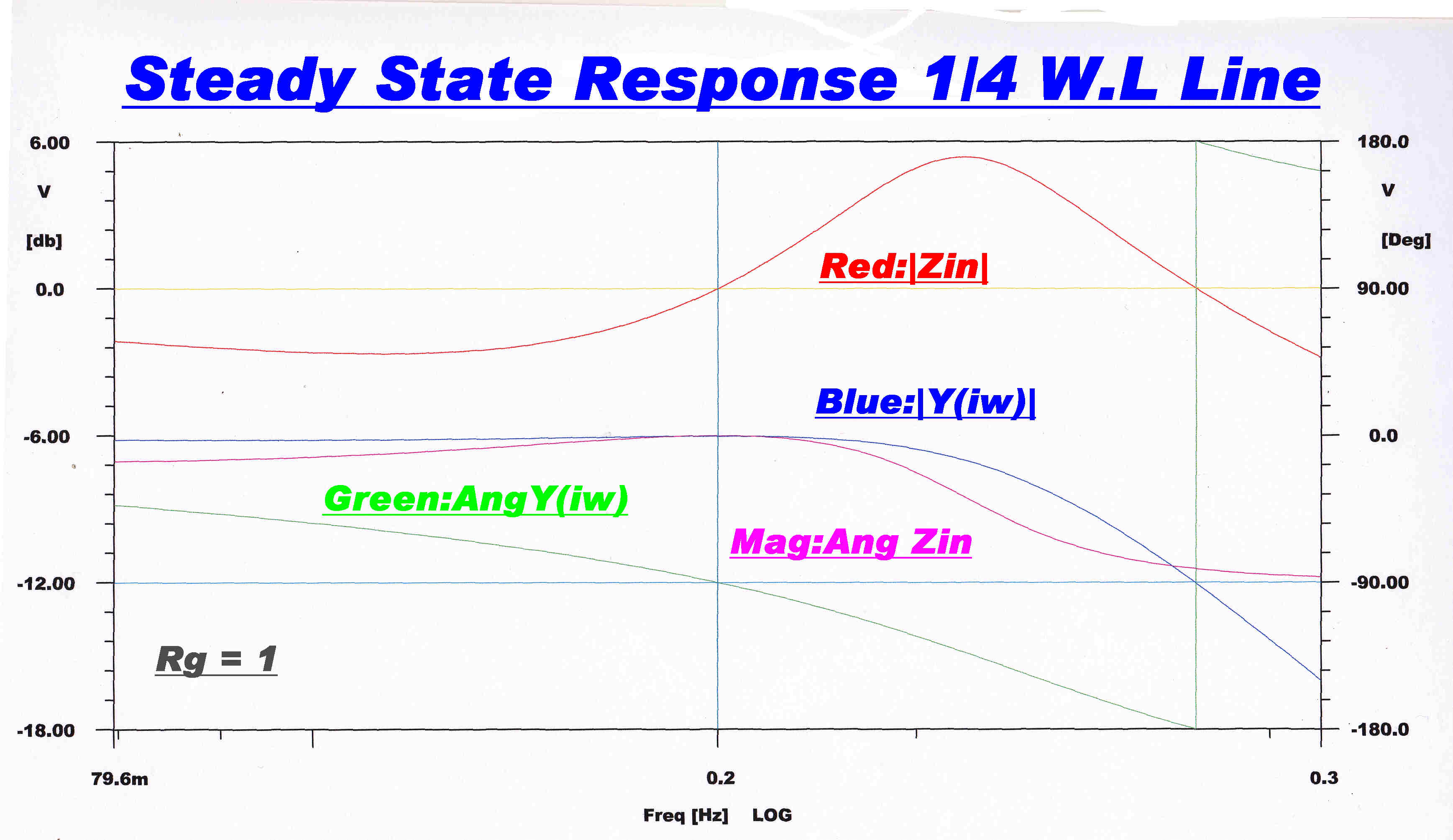
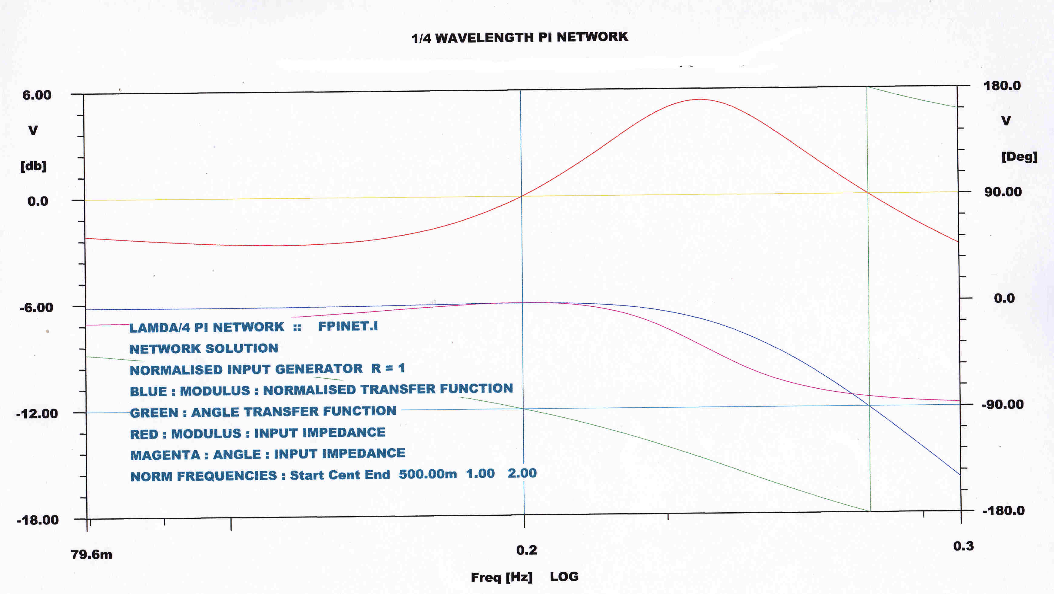
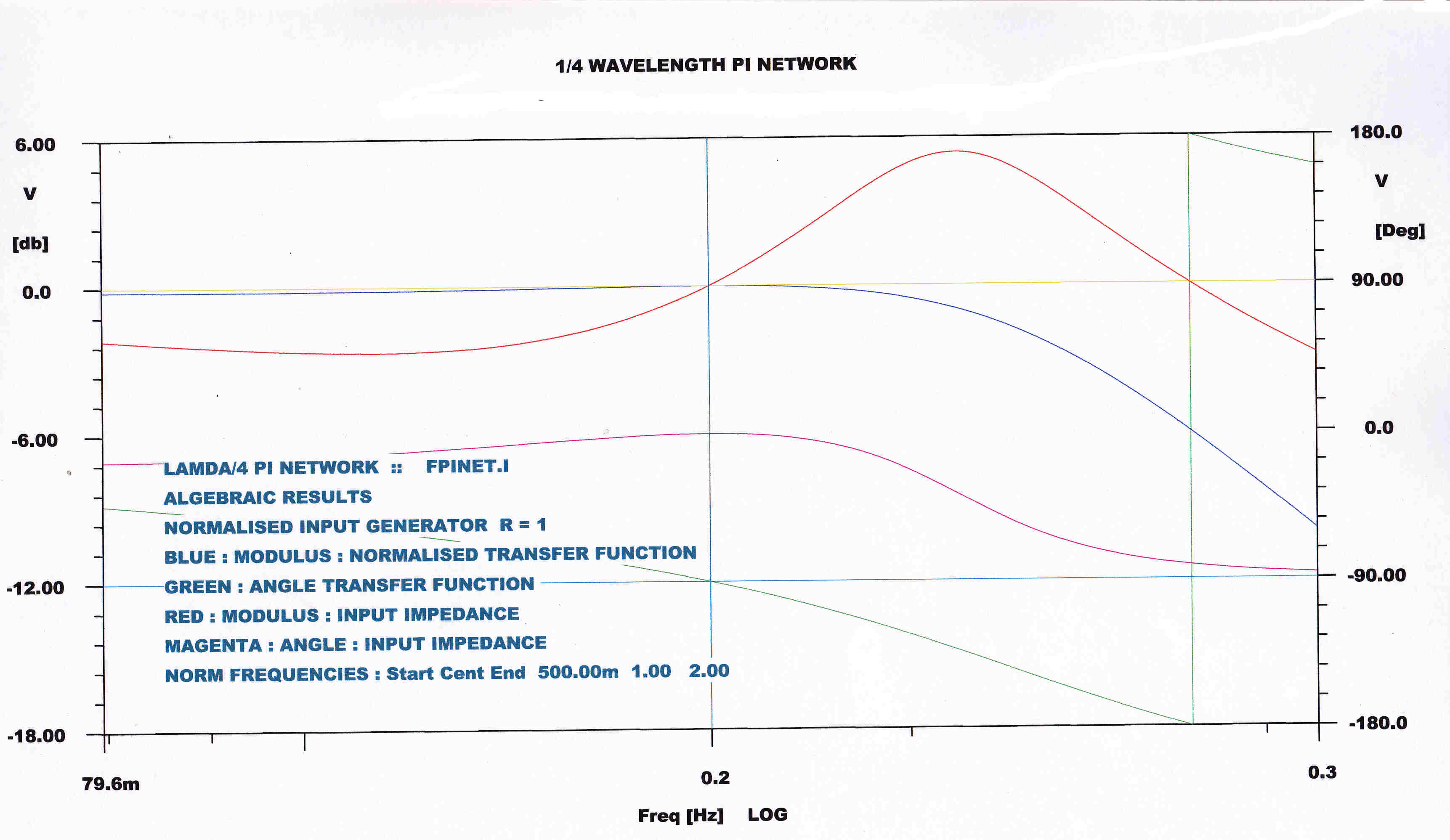
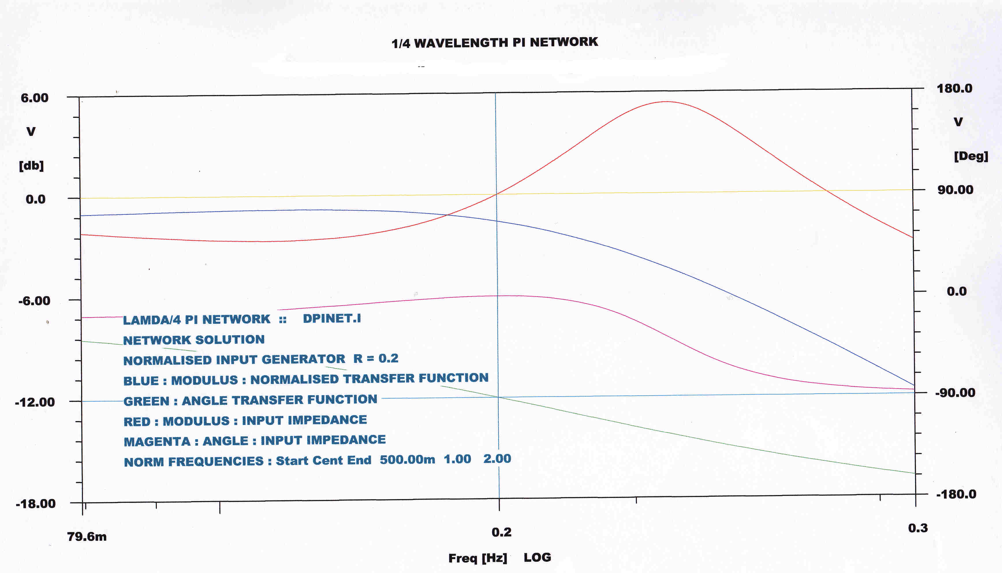
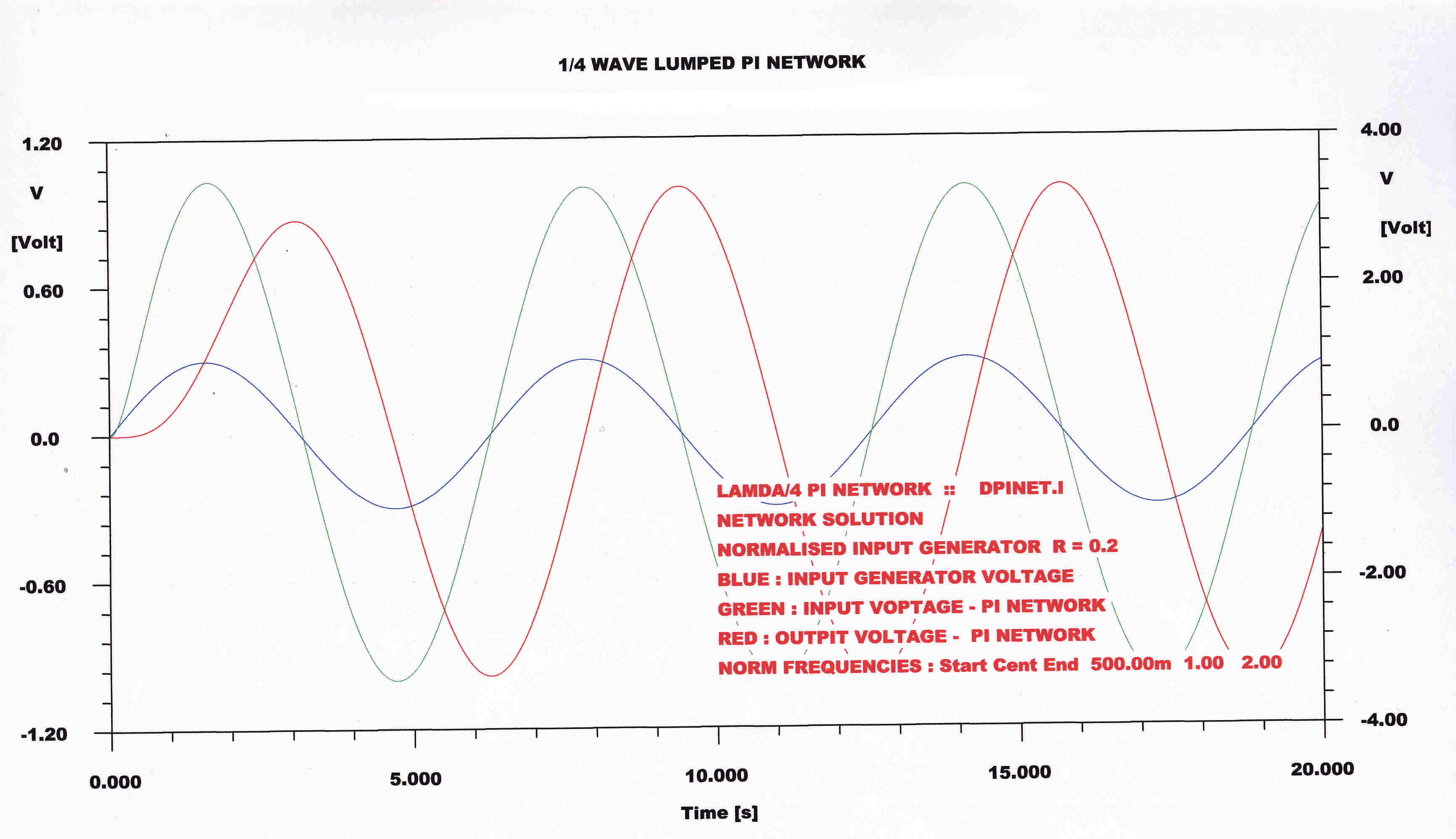
Plots for the input impedance and transfer function are given below.
They are taken from the analysis section.
The general conclusion: the bandwidth of the λ/4 network is so high it does not influence the transmitter response.
For analysis and design the normalised transfer function and input impedance are required:-
The operating frequency ω = 1 radian/sec is chosen to give the condition for the quarter wavelength ( λ/4 ) line.
The load impedance RL = 1
For the input impedance zin(p) :-
zin(p) = [ 1 + p + p2 ]/[ 1 + 2p + p2 + p3 ]
-----------(1)
For the transfer function Y(p) :-
Driven from a voltage generator of normalised output resistance k :-
Y(p) = [ 1/( 1 + k ) ]/[ 1/{ 1 + ( 1 +2k )/( 1 + k) p + p2 + k/( 1 + k ) p3 ) } ] -----------(2)
|
STEADY STATE |
|
|
 The basic network for the output stage of an Ampliphase transmitter
using the λ/4 impedance transformation is shown opposite.
The basic network for the output stage of an Ampliphase transmitter
using the λ/4 impedance transformation is shown opposite.
From the algebraic analysis developed in the analysis section, the impedance Zin seen by the LHS
plate at carrier frequency is given by:-
Zin = 2 R [ 1 + itan(φ:) ]
And the transfer function Y(iω) at carrier frequency is given by:-
Y(iω) = - i cos( φ )
where φ is the 1/2 angle of drive separation.
The modulus of the transfer function |Y(iω)| = cos( φ ) with an the angle of -90 degrees.
The modulus of the plate load is 2 R [ 1 + tan2φ ]1/2 and the angle of the
plate load Ang Zin = φ
In the RCA Ampliphase transmitter the angle φ for the carrier condition was 67.5 degrees.
Substituting for φ= 67.5 degrees in the above equations we have:-
|Zin| = 5.22 R at an angle of 67.5 degrees.
Now a vacuum tube with a highly inductive load has a low efficiency.
Capacity is paralleled across |Zin| to cancel the inductance and give a purely resistive
load at carrier.
Inductance must be paralleled across the other arm.
The symmetry of the output network is lost : a drive angle of 90 degrees no longer produces zero carrier output.
Since corrective elements are paralleled across the input to the Π network, it is convenient to work with
admittance.
The input conductance g and the susceptance b are given by:-
g = [ 1/4R ][ 1 + cos(2 φ) ] ------(2)
and similarly ::
b = [-1/4R][ sin( 2 φ ) ] ------------(3)
The corrective capacitance Ca which must be added to give a purely resistive load
for φo is given by:-
ωCa = [1/4R][ sin( 2 φo ) ] or :-
Ca = [1/(4Rω) ][ sin( 2 φo ) ] :-
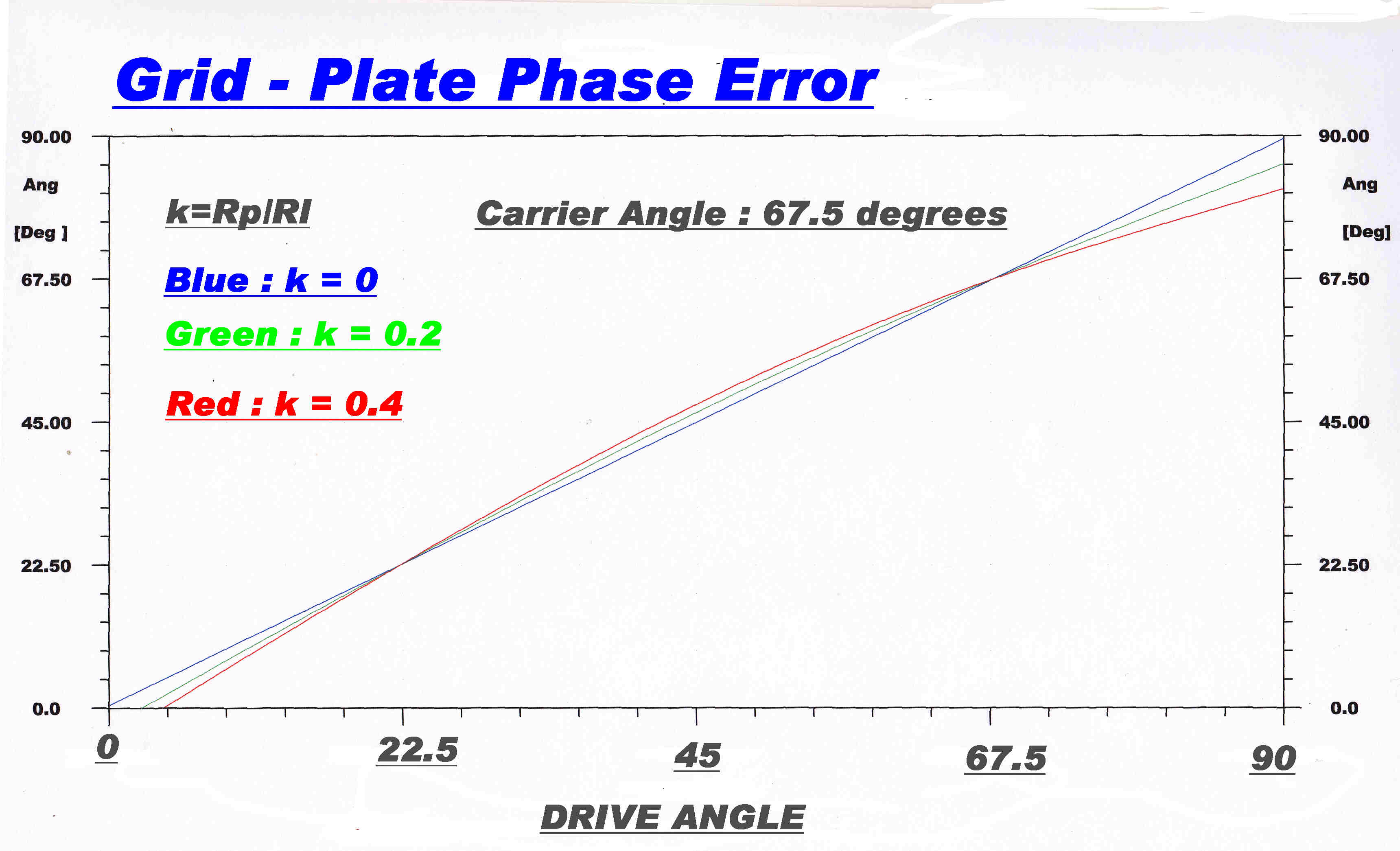 The reactive load for angles about 67.5 degrees produces a phase change betwen the grid and plate voltage.
This phase angle error increases with tubes of higher plate resistance.
The phase error modifies the cosine law.
A phase difference φ = 90 degrees no longer produces zero output.
Let k = Rp/RL where:-
Rp is e plate resistance and:-
RL is the load presented to the plate.
A plot of the grid - plate phase change is shown opposite.
The error is zero at 67.5 degrees and is maximum for k = 0.4 at φ = 90 degrees.
Phase modulation must be greater than 90 degrees to produce zero carrier.
The design philosophy of the RCA Ampliphase transmitter has always been a great puzzle to me.
The overall transfer characteristic is non-linear - a cosine law - yet great efforts were made to produce linear phase
modulation with a phase modulator which was inherently non-linear as shown in the algebraic analysis below.
It was so non-linear that three had to be used in series to approximate a linear response over +(-) 22.5 degrees.
Why not produce a modulator which had the inverse law of the transfer characteristic to give overall linearity?
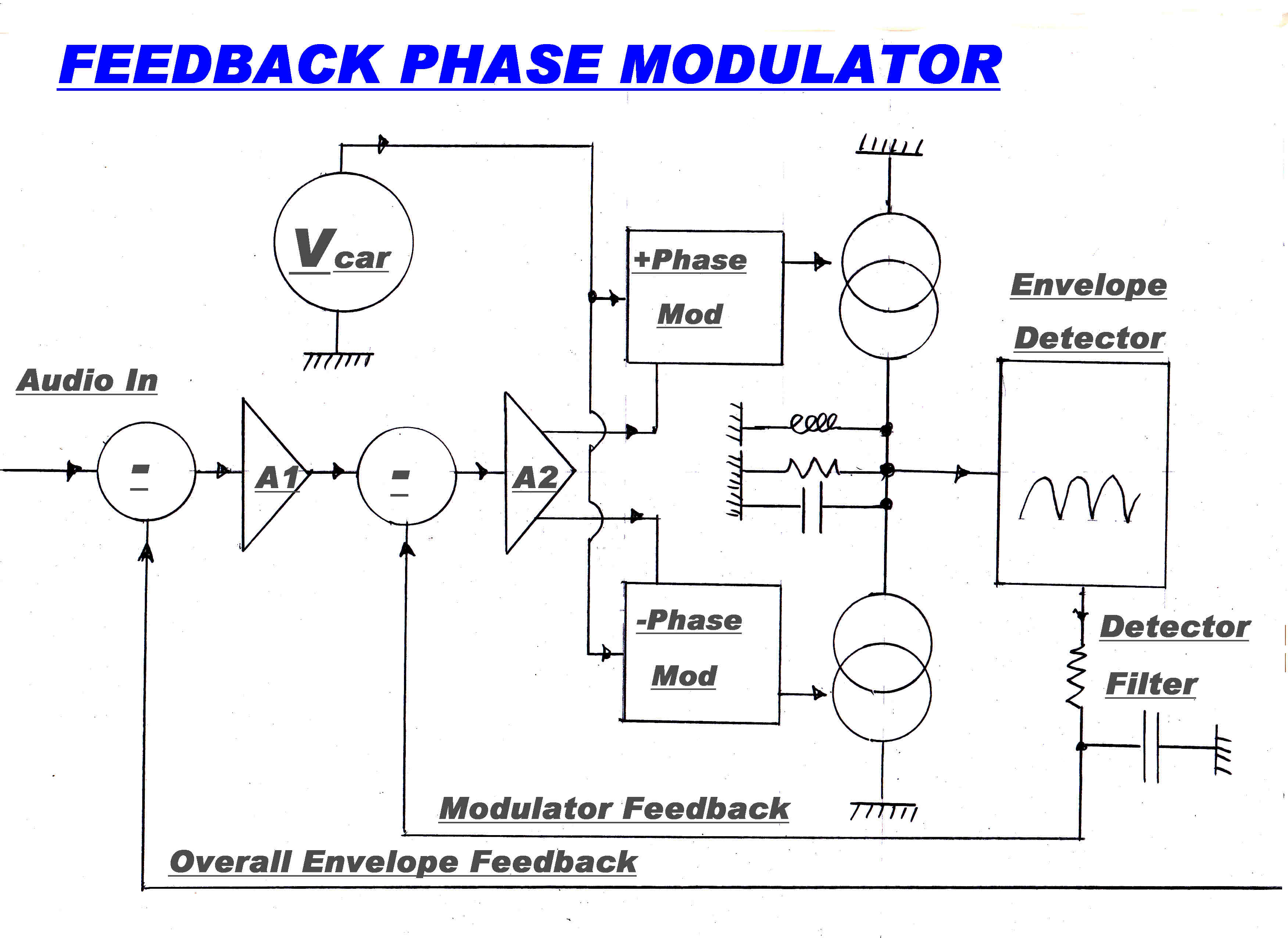 A feedback modulator to produce the complementary tansfer characteristic is shown on the right.
With heavy feedback the modulator transfer characteristic is determined solely by the transfer
characteristic of the current summing.
This can mimic the high power stage, so that the overall response is linear.
Since the system operates at a low signal level, high bandwidth receiving tubes allow for high degrees of feedback.
Simple phase modulators can be used as shown below.
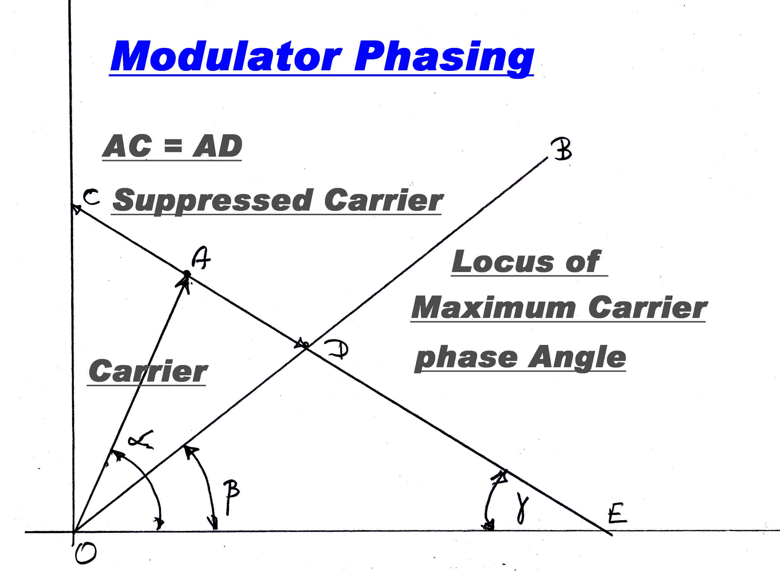 A simple phase modulator can be made by adding suppressd carrier AM to a carrier of different phase.
The phase of the two signals can be determined graphically.
A line OA is drawn at the angle α for carrier - no modulation.
A line OB is drawn at the angle β - the angle for peak modulation.
The angle γ is adjusted until AC = AD .
Symmetrical modulation of the suppressed carrier will then give the full range of phase modulation.
ANALYTICAL SOLUTION
We can now use co-ordinate geometry to get an analytical solution for the angle γ of the suppressed carrier modulation.
Given:the angle at carrier: α
the angle for zero modulation: 0
the angle for 100% modulation: β
the signal from the suppressed carrier modulator is symmetrical and we want to find the angle γ which will just take the
phase from 0 to β
The suppressed carrier angle passes through the point A.
We want to evaluate the angle γ which will make AC = AD
Equation for the line OA
y = x tan(α) --------------[1]
For OB:
y = x tan(β) ---------------[2]
Now make the carrier unity amplitude 1 so that OA = 1
The coordinates of OA are then x = cos(α) : y = sin(α)
Now ADE must pass through the point A with a gradient of tan(γ) so :
[ y - sin(α) ]/[ x - cos(α) ] = tan(γ)
which gives:
y = ( x - cos(α) )tan(γ) + sin(α) ----------[3]
The point of intersection D id given when y[3] = y[2]
So: xDtan(β) = ( x D - cos(α) )tan(γ) + sin(α)
which gives:
xD = [ sin(α) - cos(α) tan(γ) ]/[ tan(β) - tan(γ) ]
Now AC = AD so :
xD = 2 cos( α ) so :
2 cos( α ) = [ sin(α) - cos(α) tan(γ) ]/[ tan(β) - tan(γ) ]
After some algebra we have:
tan{γ) = 2 tan(β) - tan(α)
For the magnitude of the suppressed carrier AD :
AO cos(α) = AC cos(γ)
AC = AO [ cos(α) ]/[ cos(γ) ]
If AO = 1 , then :
Normalised suppressed carrier amplitude = [ cos(α) ]/[ cos(γ) ]
NUMERICAL EXAMPLES
If α = 60 deg : β = 0 : γ = -60 degrees : Anorm = 1
If α = 67.5 deg : β = 45 deg : γ = -22.5 deg : A norm = 0.4142
Under Construction.
Under Construction.
Phase modulation occurs at a low power level in an ampliphase transmitter.
There are usually two or three RF power amplifying stages between the low level modulator and the
final stage.
It is necessary to evaluate the dynamic response of the RF stages to the phase modulation:-
[A] To evaluate the overall response of the transmitter.
[B] To investigate the stability of envelope feedback loops and design stabilising networks if necessary.
It is easy to show algebraically that the response of a linear network to a phase modulated signal is
the same as that for an amplitude modulated signal if the phase modulation is small.
A large phase modulation index - say of Π radians - throws up a non-linear differential equaton
which can only be solved by numerical methods.
It will be shown that the linear approximation holds for the phase deviations encountered in
ampliphase transmitters - typically Π/4 radians.
We now show that the AM and PM responses of a linear network are identical if the PM phase deviation is small.
The phase deviation is considered small if tan(φ) ≈ φ
Consider the signal Vin transmitted through a linear network where :-
Vin =
m sin[ ωct + ωmt ] + m sin[ ωct - ωmt ]
If the network has a symmetrical steady state response about ωc normalised to:-
|Y(iωc)| = 1 and Ang:Y(iωc) = 0
Y(iωc + iωm) = A Ang(α)
Y(iωc - iωm) = A Ang(-α)
The output Vout will be:-
Vout =
A m sin[ ωct + (ωmt + α) ]
+ A m sin[ ωct - (ωmt + α) ]
Now we have the identity:-
sin( a + b ) + sin( a - b ) = 2sin( a ) cos( b )
So:-
Vout = [ sin( ωct ) ][ 2 A m cos( ωmt + α ) ]
This is a carrier suppressed AM wave.
Because the network is linear, superposition can be applied and we can now transmit either a signal
sin(ωct) or cos(ωct) and add it to Vout
The addition of sin(ωct) gives an AM signal:-
Vam = [ sin(ωct) ][ 1 + 2 m A cos( ωmt + α ) ]
The addition of cos(ωct) to Vout gives a signal with both AM and PM modulation:-
Vam = [ cos(ωct) ] +
[ sin( ωct ) ][ 2 A m cos( ωmt + α ) ]
= |V|cos( ωt + φ ) where :-
|V| = [ 2 A m cos( ωmt + α ) ]2
= 4 A2 m2 cos2( ωmt + α )
tan(φ) = 2 A m cos( ωmt + α )
If φ << Π/4 then:-
tan(φ) ≈ φ
and we have for the phase modulation φ
φ = 2 A m cos( ωmt + α )
which is also the response to the amplitude modulation.
Substituting in the equation for |V|:-
|V| = [ 1 + 4 A2 m2 cos2( ωmt + α ) ] 1/2
if m A is small :-
|V| ≈ [ 1 + 2 A2 m2 cos2( ωmt + α ) ]
But cos2( ωmt + α ) = [1/2][ 1 + cos2( ωmt + α ) ]
So :-
|V| ≈ [ 1 + 2 A2 m2 (1/2)( 1 + cos2( ωmt + α ) ]
So there is also a small amount of second harmonic amplitude modulation of amplitude A2 m2
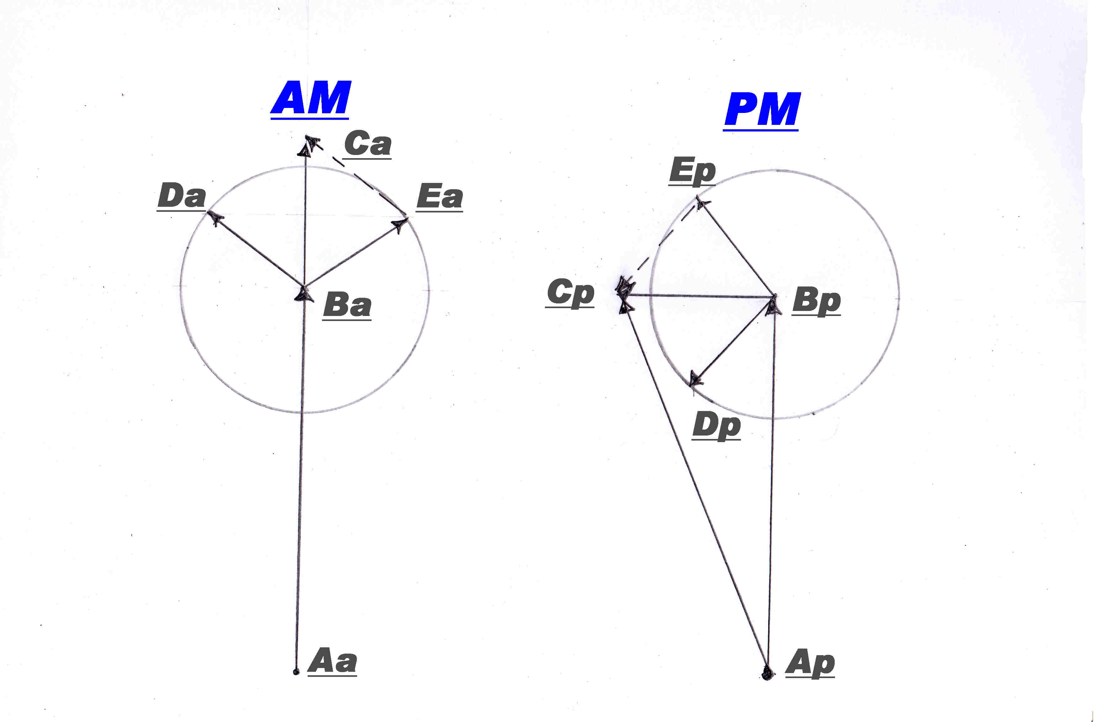 A gometric interpretation of the algebraic equations derived above is shown opposite.
The usual phasor or vector diagram used to describe steady state circuit response is valid only
for single frequencies.
Modulated signals are dynamic - not composed of a single frequency - and require an extended interpretation.
Imagine the three sidebands of an AM signal produced by three single phase generators in series.
The angular velocity of the carrier generator will be ωc
the upper sideband generator [ ωc + ωm ]
the lower sideband generator [ ωc - ωm ]
If we draw diagonals across the armatures of the alternators and project down to the X axis, then the line on the x axis
represents the instantaneous output of the generators and the instantaneous value of the AM wave.
We can slow the whole thing down and make the carrier generator armature stationary by rotating the whole system backwards
at ωc
The armature of the upper sideband generator will then rotate at ωm in one direction
and the lower sideband at ωm in the other.
Two equal vectors rotating with the equal and opposite angular velocities produce a vector whose magnitude
varies sinusoidally and always in the same direction bisecting the two.
This is a suppressed carrier wave.
Adding this to a wave of the same phase and frequency produces pure AM.
Adding to a wave displaced by 90 degrees produces both phase and amplitude modulation.
Da-Ba : Ea-Ba and Dp-Bp : Ep-Bp are the rotating vectors producing the sinusoidally varying
vectors of constant phase Ba-Ca and Bp-Cp.
When added to an in phase carrier Aa-Ba, the magnitude of Aa-Ca varies in amplitude aith a
constant phase producing pure AM.
When added to a quadrature carrier Ap-Bp, the output Ap-Cp varies in phase and amplitude
producing both PM and AM.
The angle of Ap-Cp varies at ωc rate and is very nearly sinusoidal if
[Bp-Cp]/[Bp-Ap] is small giving rise to PM with low distortion.
The length of Ap-Cp varies at 2 ω giving complete second harmonic distortion on the AM
component of the wave.
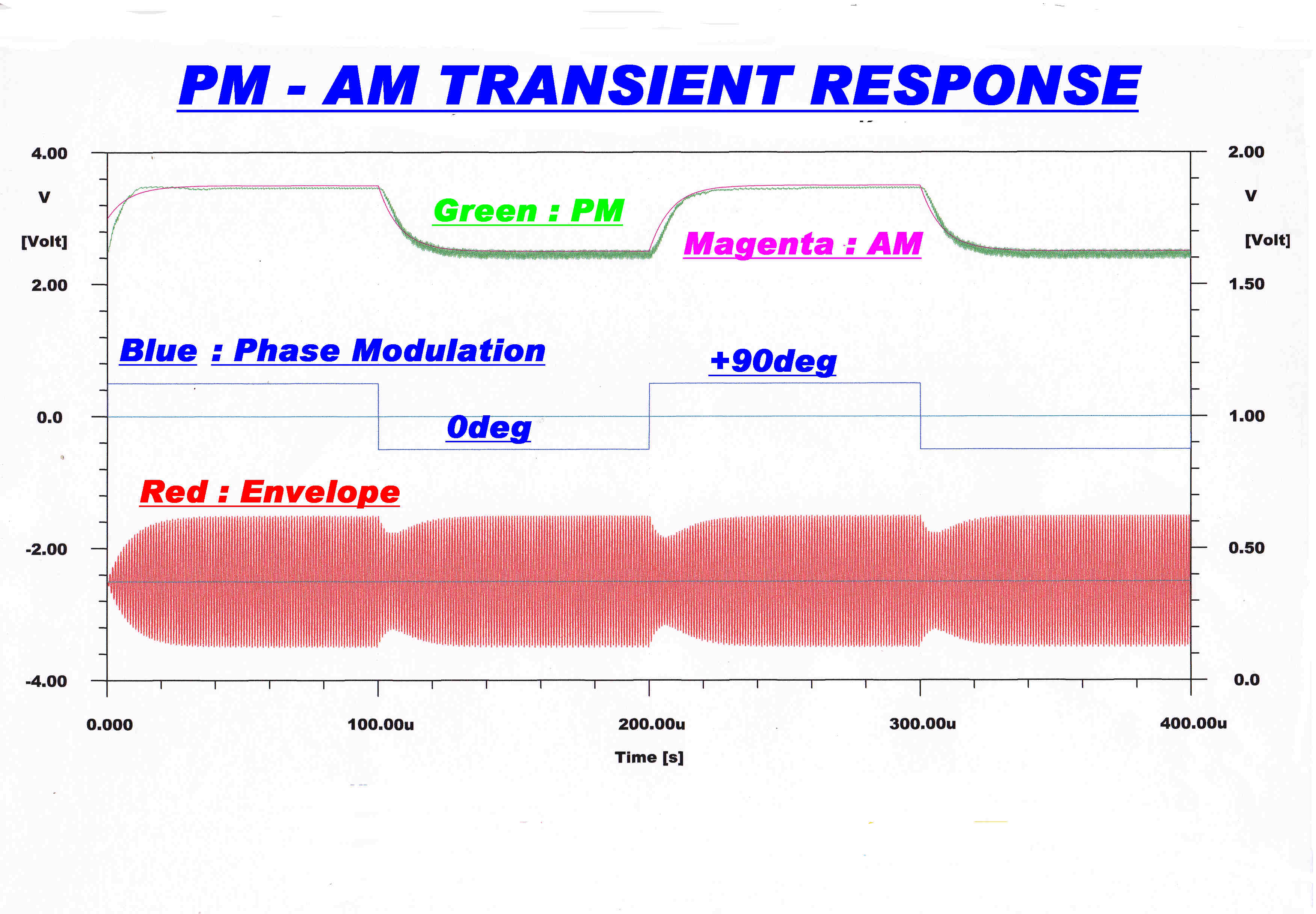
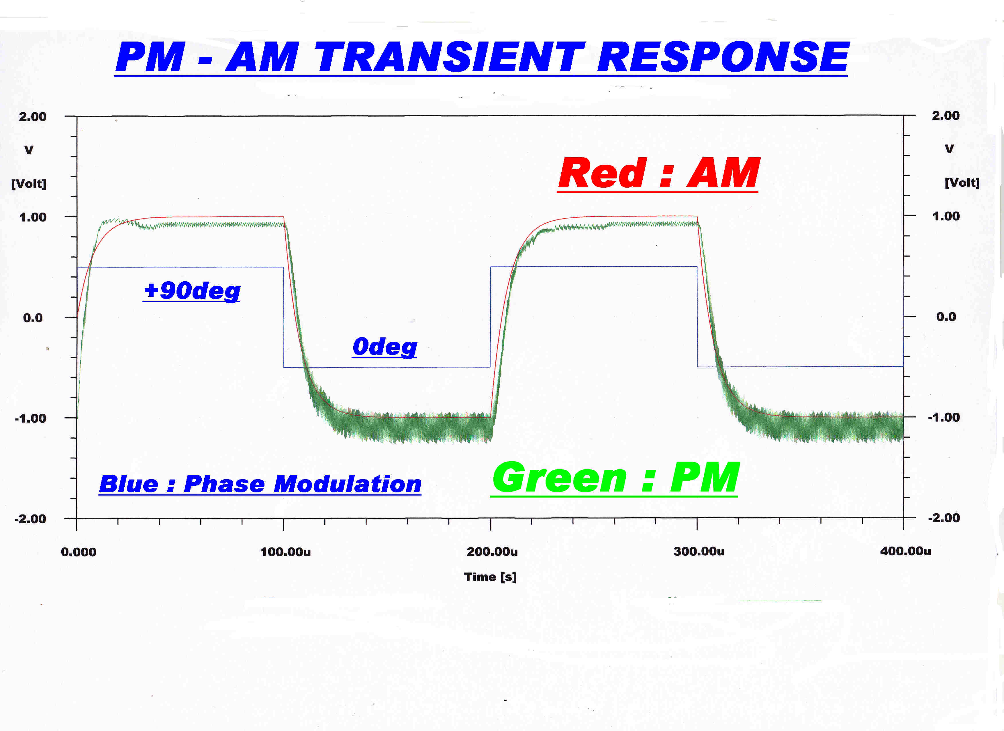
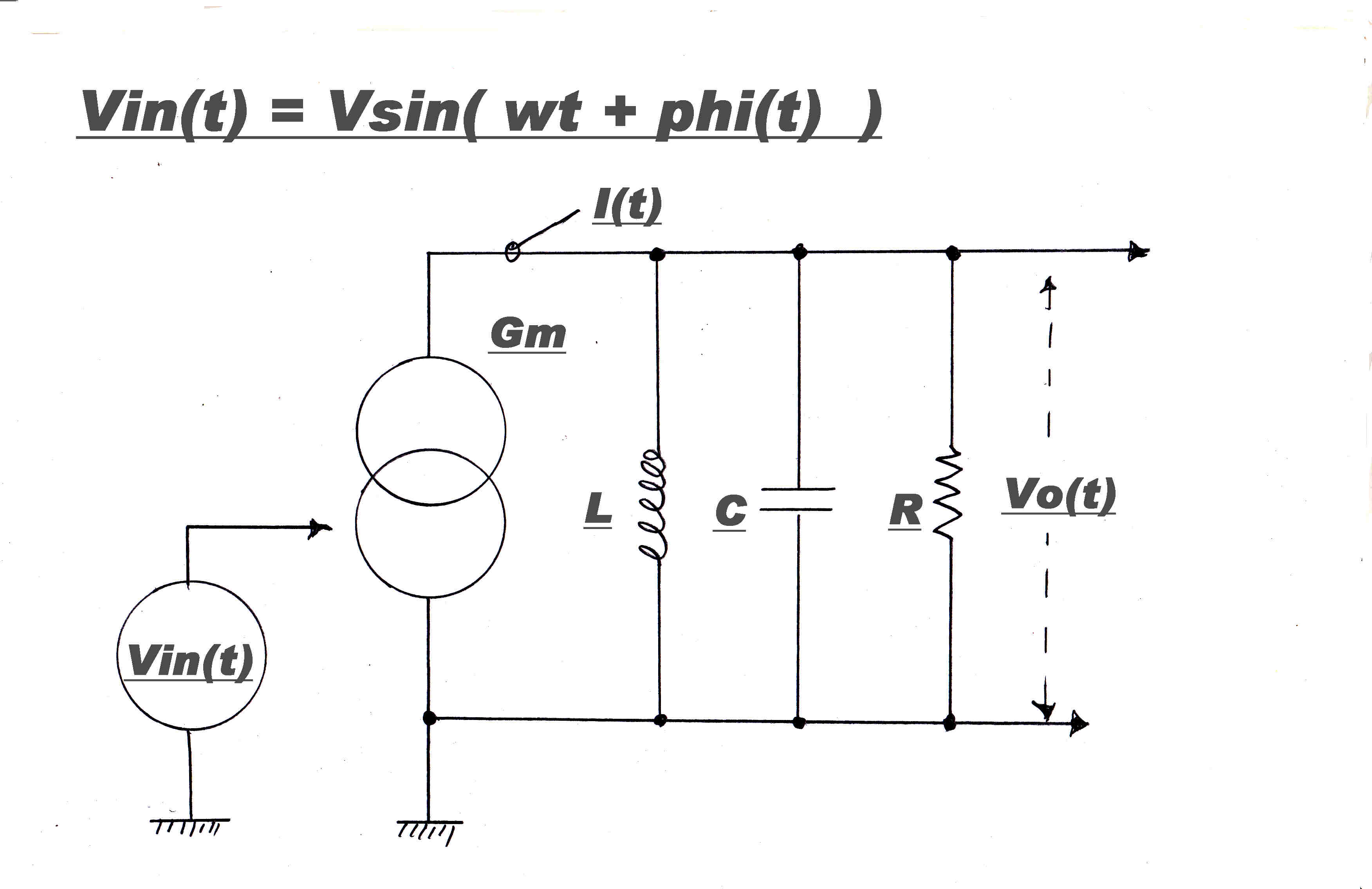 A parallel tuned circuit representing the coupling network between RF stages
in an Ampliphase transmitter is shown opposite.
A parallel tuned circuit representing the coupling network between RF stages
in an Ampliphase transmitter is shown opposite.
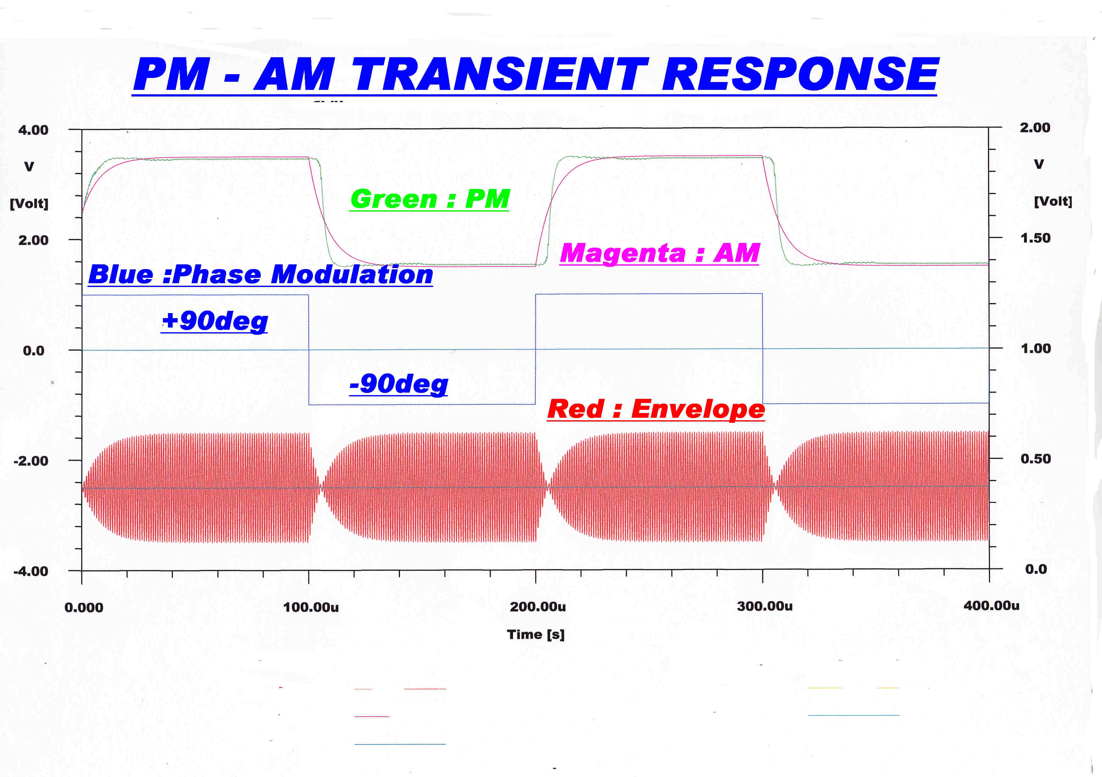
Below are shown the responses of this network to an amplitude and phase modulated wave.
The amplitude response is governed by a linear differential equation and the algebraic
solution is plotted.
The numerical solution is given for the phase response.
For a phase modulation index of Π/2 radians there is virtually no difference between the
AM and PM response.
Fortunately, the maximum phase deviation used in Ampliphase transmitters does
not exceed Π/2 radians. In the RCA ampliphase transmitters the maximum phase deviation
was +(-) Π/8 radians.
|
|
|
Blue :Modulating Signal |
Blue :Modulating Signal |
|
|
|
Blue :Modulating Signal |
Blue :Modulating Signal |
 The circuit is shown on the right.
The λ/4 Π network is the basic building block of the Ampliphase and Doherty high efficiency output networks.
It mimics the behaviour of a λ/4 (quarter wavelength ) line at one frequency f
where λ = c/4 f c = velocity of light.
For the λ/4 condition:-
1/ωC = ωL = R
If we normalise both angular frequency and impedance level:-
ω = 1 : R = 1
So 1/C = L = R = 1
k becomes the fractional driving resistance.
In practice this would be the output resistance of the final tube.
Since the input resistance to the network is R ( = 1 ), the signal is attenuated by 1/( 1 + k )
If the output is short circuited, L resonates with the input C to form a parallel tuned circuit producing an infinite input impedance.
If the output is open circuited by removing R, L forms a series resonant tuned circuit with the output C to produce zero input impedance.
At frequency f there is a phase change of -90 degrees through the network.
So if Vin = Vcos( 2 Π f t) then Vout = Vsin( 2 Π f t)
This is the behaviour of a quarter wavelength line.
The transmitter output stage is not confined to one frequency under modulation, so it is necessary to study the steady state
and dynamic behaviour over a range of frequencies.
For analysis and design the normalised transfer function and input impedance are required:-
For the input impedance zin(p) :-
zin(p) = [ 1 + p + p2 ]/[ 1 + 2p + p2 + p3 ] -----------(1)
For the transfer function Y(p) :-
Y(p) = [ 1/( 1 + k ) ]/[ 1/{ 1 + ( 1 +2k )/( 1 + k) p + p2 + k/( 1 + k ) p3 ) } ] -----------(2)
The steady state transfer function and input impedance are plotted over a wide bandwidth
of 1/2 the carrier frequency.
Both the direct digital computer and algebraic solutions are plotted.
|
|
|
The magnitude of the transfer function has fallen to 1/2 at centre frequency. |
The plot from the operational equations (1) and (2 ) above is identical with the computer
solutions : establishing their veracity. |
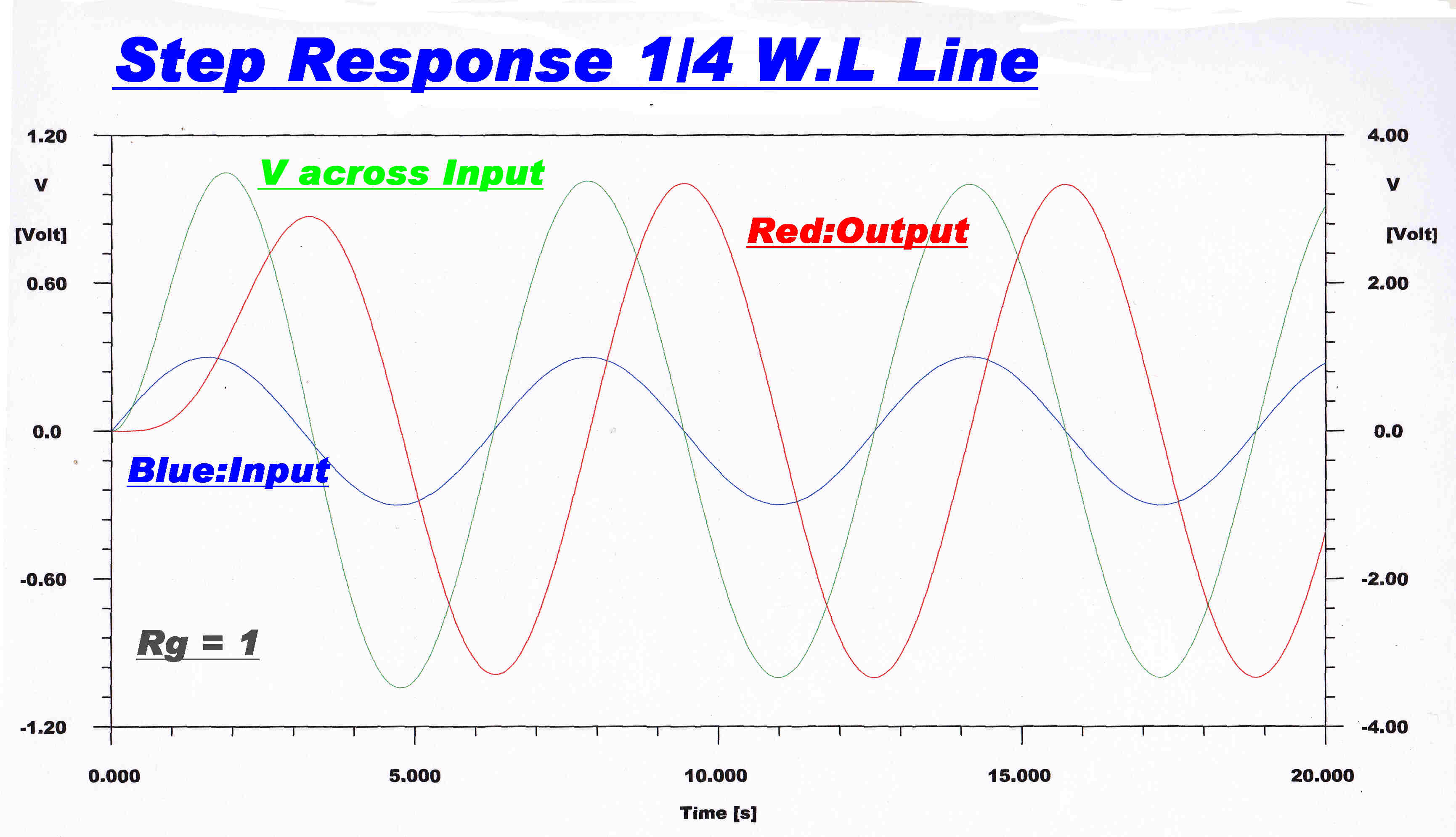
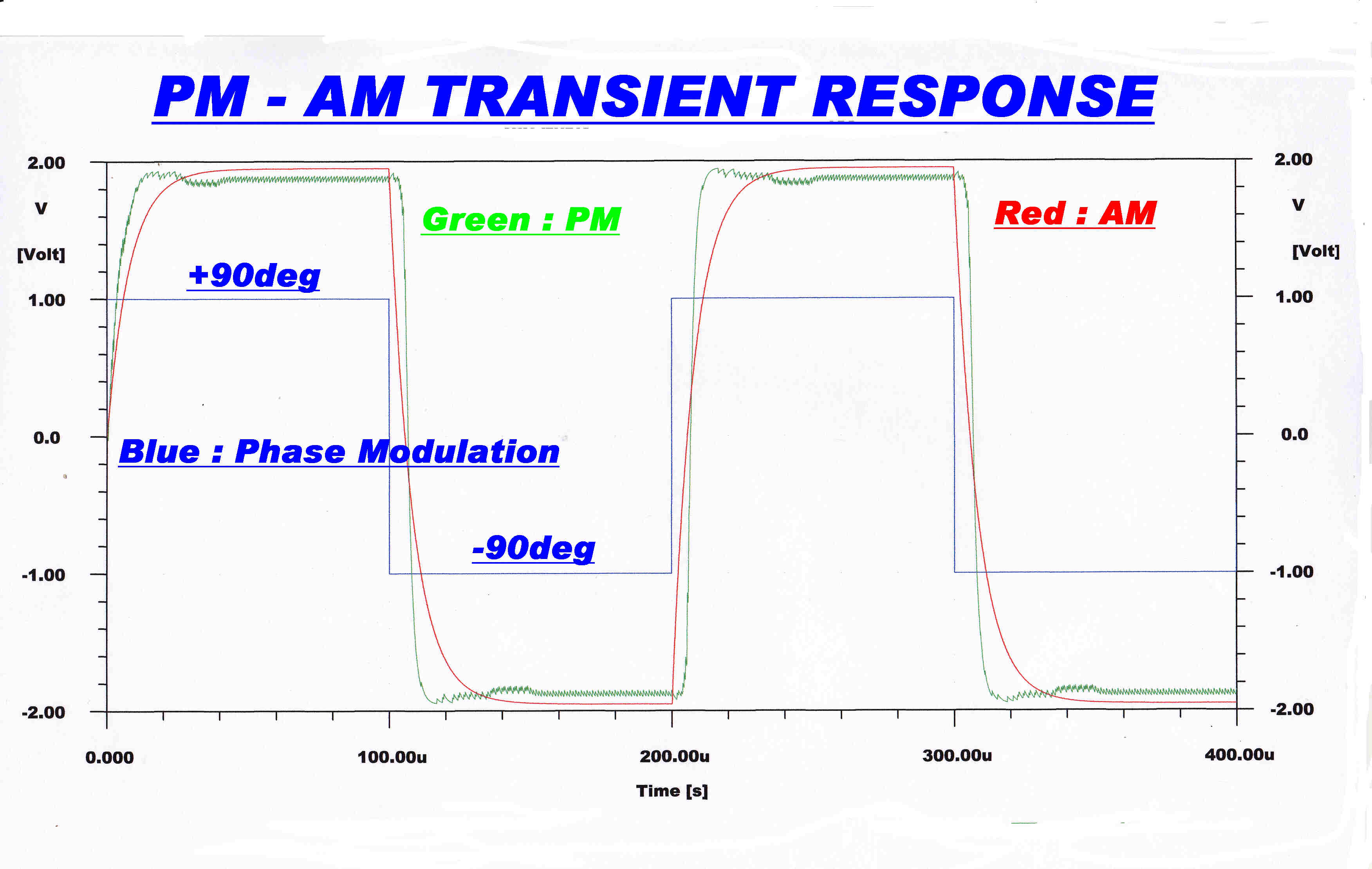
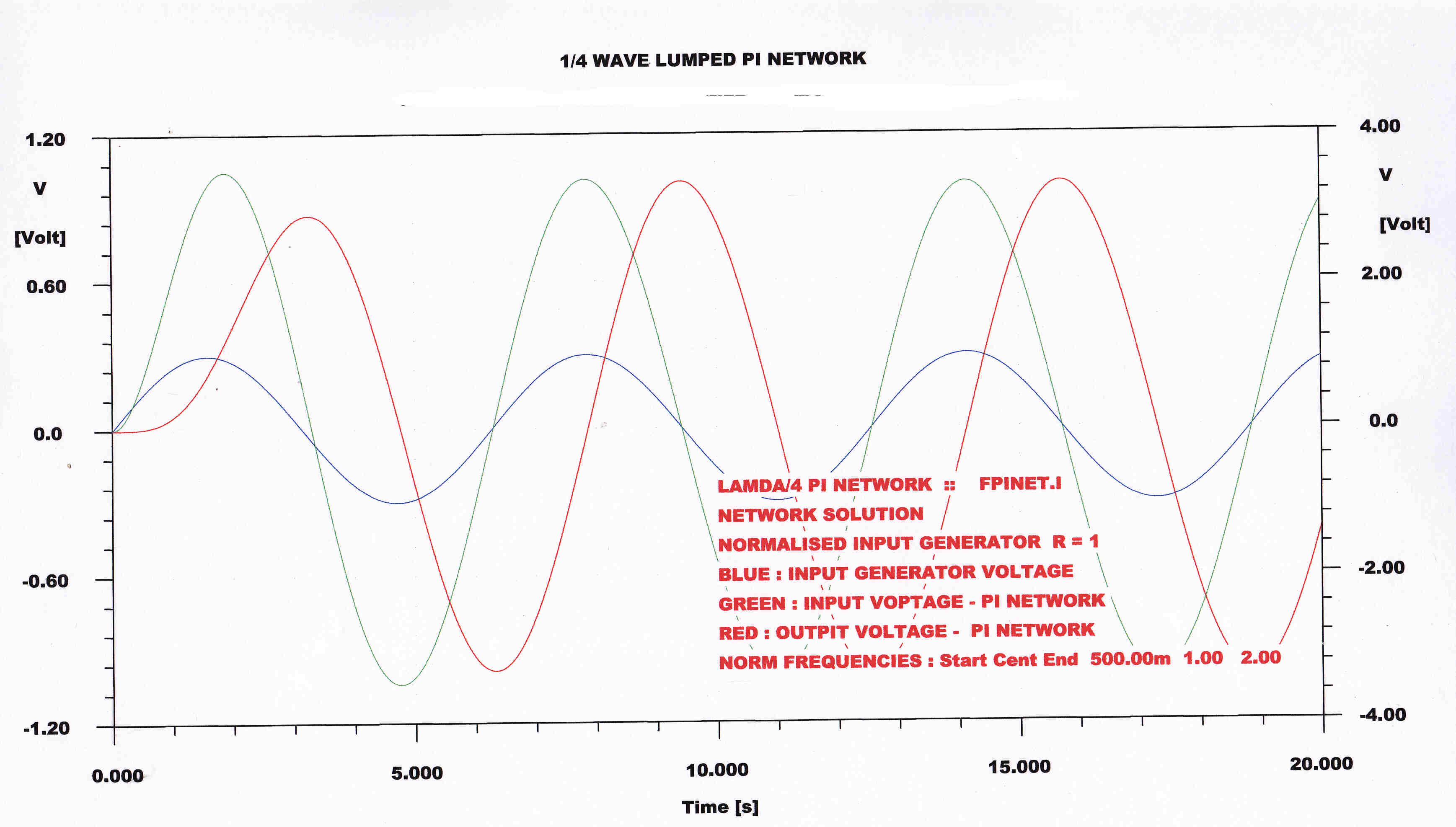
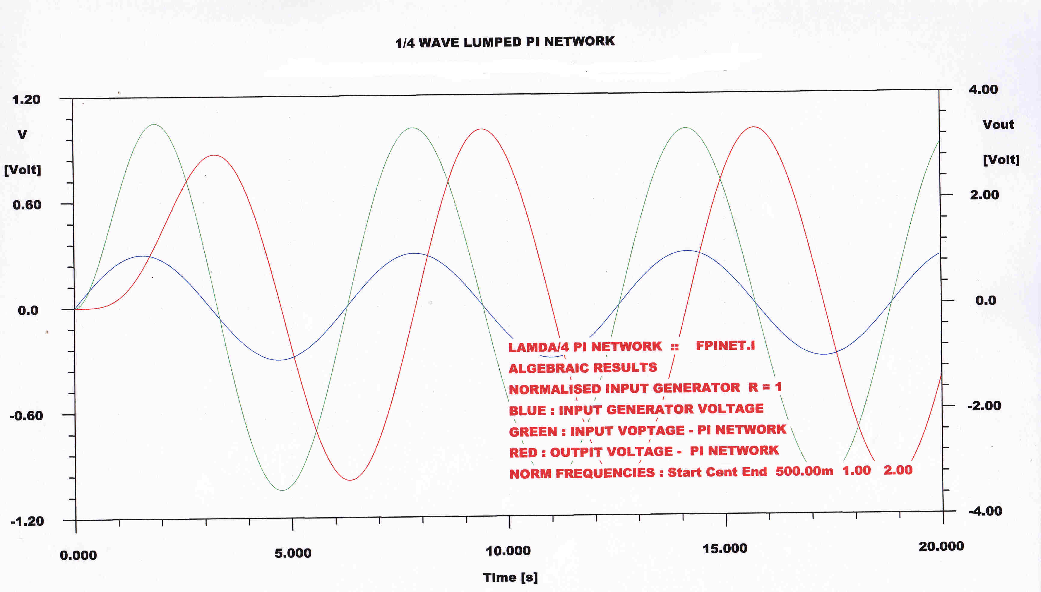
The transient response to a step function of amplitude modulation is plotted
The carrier is at the center frequency f.
Note: The transient response of any network is the same for amplitude and phase modulation if the phase
deviation is small.
Both the direct digital computer and algebraic solutions are plotted.
|
|
|
The output voltage is 90 degrees behing the input. |
The solution from the algebraic equations is identical with the computed network solution. |
The steady state and transient responses are plotted for k = 0.2
This would be a typical value for a high power triode in the output stage.
|
|
|
Blue: Input Step Function on The Carrier |
Blue: Input Step Function on The Carrier |
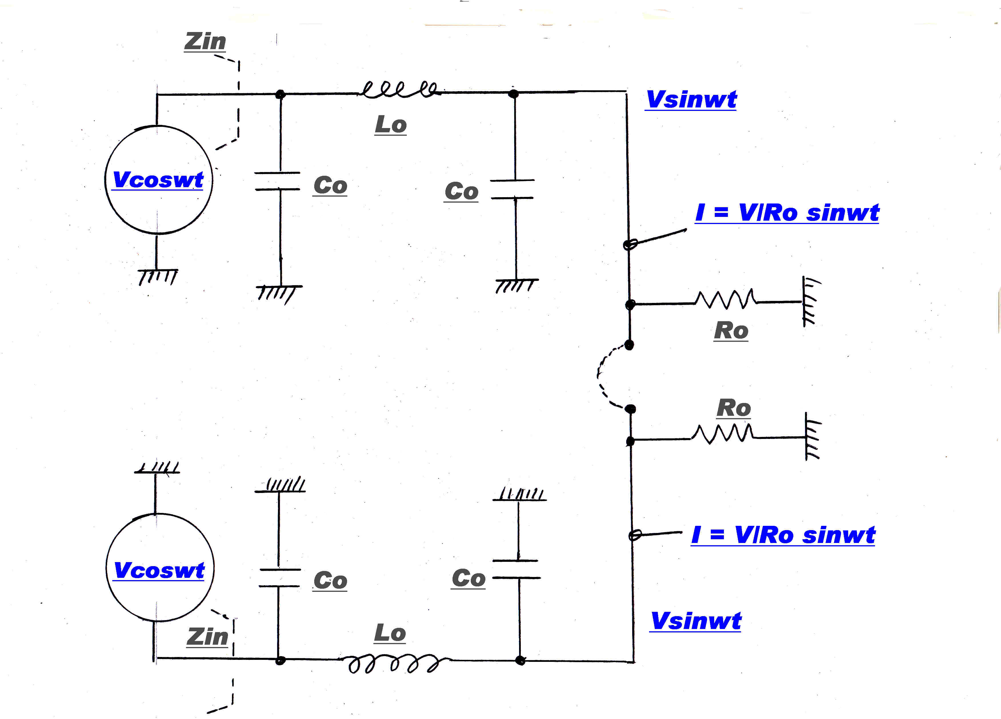 Imagine the link broken, so that we have two identical λ/4 Π networks Lo Co Co terminated in their characteristic
impedance Ro.
Imagine the link broken, so that we have two identical λ/4 Π networks Lo Co Co terminated in their characteristic
impedance Ro.
Circuit analysis shows that, If the networks are driven from identical generators Vcos(ωt), the terminating voltage will be Vsin(ωt)
(to allow for the 90 degree lag in the network.)
The voltages at all nodes of the network will be the same, so that corresponding nodes may be joined without disturbing the network.
Close the link.
The terminating impedance will now be Ro/2 , the output voltage Vsin(ωt), and the load current [ 2/Ro ] Vsin(ωt)
If the input voltages are equal and opposite say Vcos(ωt) and -Vcos(ωt) then,
because of the symmetry of the networks,
the output voltage across Ro will be zero.
This is an important point.
In an Ampliphase transmitter inductors and capacitors are shunted across opposite sides of the network to modify the input impedance.
This destroys the symmetry of the network.
Then equal and opposite voltages do NOT produce zero output.
 TRANSFER FUNCTION MODULUS
Take the circuit with the switches as shown.
Now drive each side with the voltage generators
Vsin(ωt + φ ) and Vsin(ωt - φ )
These generators can be resolved into two equivalent generators:-
Vsin(ωt + φ ) = [ Vcos(φ) ] sin(ωt) and [Vsin( φ )]cos(ωt)
and
Vsin(ωt + φ ) = [ Vcos(φ) ] sin(ωt) and - [Vsin( φ )]cos(ωt)
The switches may now change without altering the circuit in any way.
By superposition in a linear circuit, the two generators produce current independently, so we have:-
[1] The two equal voltages [ Vcos(φ) ] sin(ωt) will produce the voltage [ Vcos(φ) ][ - cos(ωt) ]across
the output load Ro .
[2] The modulus of the transfer function then must be cos(φ) since only the [ Vcos(φ) ] sin(ωt) generators
can produce output.
|Vout| = |Vin| cos(φ)
[3] The two equal and opposite voltages will always produce zero volts across the load Ro.
[4] We can short circuit the load if it has zero volts across it without any disturbance. The inductor Lo
is then short circuited to earth and forms a parallel tuned circuit with Co to give an infinite input impedance
at carrier frequency for :-
fo = 1/2 Π [ LoCo ]1/2
Equal and opposite voltage generators produce NO input current.
INPUT IMPEDANCE :: INPUT ADMITTANCE
Since the out of phase generators can produce no input current, the current Iin is given by:-
Iin = [1/Ro][ Vcos(φ) ] sin(ωt)
for an input voltage Vsin(ωt + φ )
It is now convenient to move to complex notation to perform the steady state analysis.
Vsin(ωt + φ ) becomes Veiφ = Vcos(φ ) + i sin( φ ) = Vin
Iin = [V/Ro]cos(φ:)
Rin = Vin/Iin = Ro [ Vcos(φ ) + i sin( φ ) ]/[ Vcos(φ:) ]
= Ro [ 1 + i tan(φ:) ]
So:- Rin = Ro [ 1 + i tan(φ:) ] ---------(1)
In an ampliphase transmitter compensating elements are added in parallel across the inputs, so it is more
convenient to have equation (1) expressed as an admittance yin
yin = 1/Rin = 1/ Ro [ 1 + i tan(φ:) ]
= [ 1/Ro][ 1 - i tan(φ) ]/[ 1 + tan2(φ) ]
= [ 1/Ro]/[ 1 + tan2(φ) ] - [ i tan(φ)]/[ 1 + tan2(φ) ]
Now yin = g + i b
where g = [ 1/Ro]/[ 1 + tan2(φ) ] and b = - [ i tan(φ)]/[ 1 + tan2(φ) ]
Examining g :: g = [ 1/Ro]/[ 1 + sin2(φ)/cos2(φ) ]
g = [cos2(φ)]/Ro
But cos2(φ) = 1 + cos( 2 φ )
So ::
g = [ 1/2Ro ][ 1 + cos(2 φ) ] ------(2)
and similarly ::
b = [-1/2Ro][ sin( 2 φ ) ] ------------(3)
NOW TEST THESE EQUATIONS AT LIMITS
When φ = 0
g = 1/Ro OK
b = 0 OK
When φ = 90 degrees
g = 0 OK
b = 0 OK
It turns out that the equations agree with the direct digital analysis of the circuit.
RCA EQUATIONS
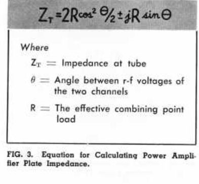 The equations shown opposite are given in an RCA article on the AMPLIPHASE TRANSMITTER*
* D R Musson
Broadcast News Vol. 119 Feb. 1964
The equations seem to fail at the limits:-
If Θ = 0 then ZT = 2R OK
If Θ = 180 then ZT = 0 NOT OK : should be infinity
Note different definitions of R and Θ from ones used in my equations above.
 DESCRIPTION
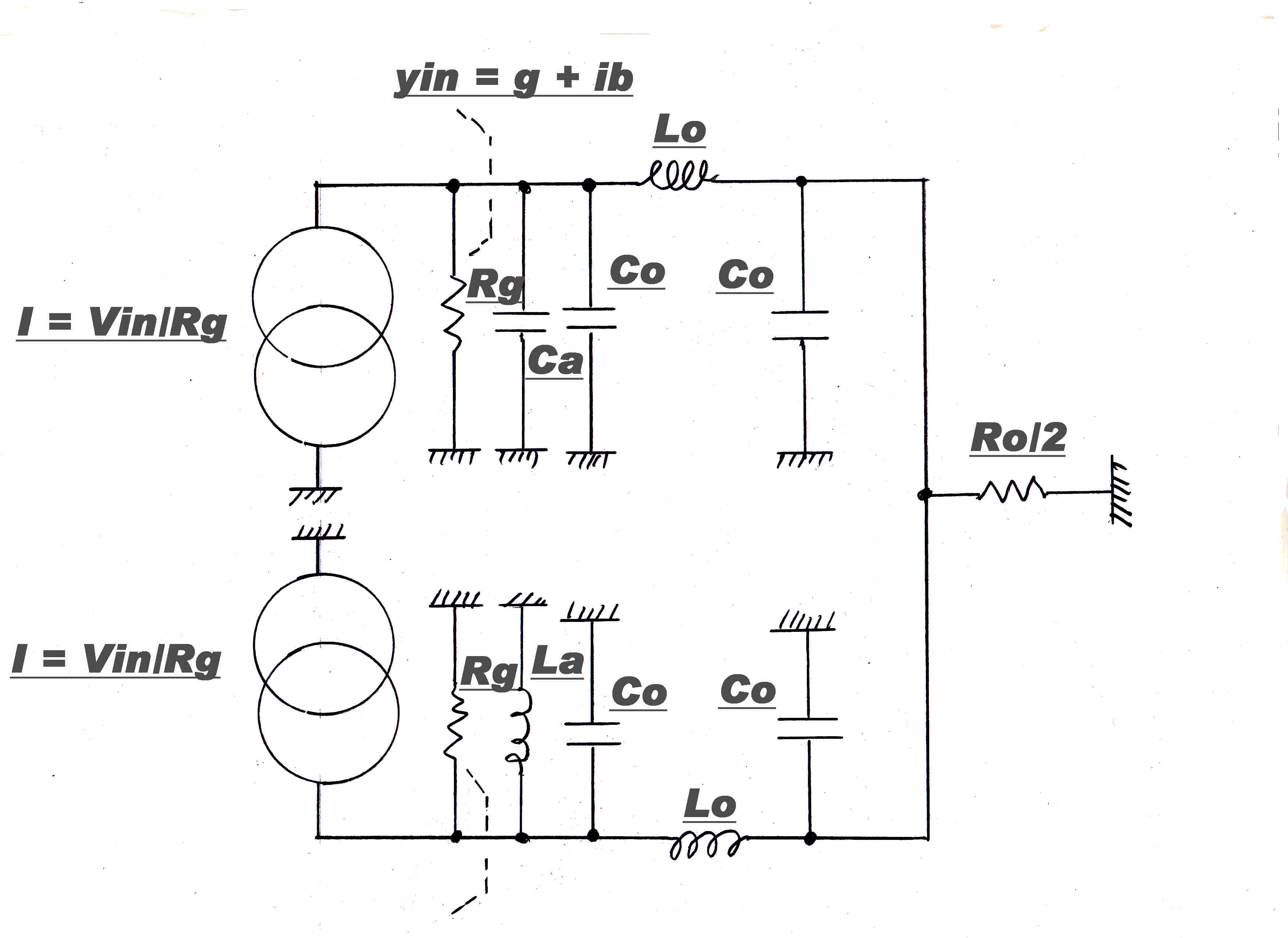
The circuit representing the output stage of an Ampliphase transmitter is shown opposite.
It departs from the circuits analysed above in two ways:-
[A] The capacitor Ca and inductor La are shunted across the inputs of the λ/4 networks
to modify the input impedance.
These additions make the input impedance purely resistive at some designated drive
angle Θ - usually 67.5 degrees.
They also destroy the symmetry of the network.
If an output resistance Rg is now added to the voltage generator, the asymmetry will now
manifest itself.
Equal and opposite input voltages will no longer cancel across the output load Ro/2.
[B] The networks are driven by vacuum tubes.
These are not pure voltage generators, but have an output resistance Rg
This introduces a further complication in design:-
The angle of the voltage on the plate differs from the grid drive angle.
ANALYSIS
From above the input conductance and susceptance are given by:-
g = [ 1/2Ro ][ 1 + cos(2 φ) ] ------(2)
and
b = [-1/2Ro][ sin( 2 φ ) ] ------------(3)
If we want to cancel the susceptance to produce a purely resistive input for a drive angle Θ
at a frequency ω then we must add a susceptance ba where :-
ba = [1/2Ro][ sin( 2 Θ ) ] = ωCa
So that :-
Ca= [1/2 ω Ro][ sin( 2 Θ ) ]
Similarly on the other side we must add La in parallel where :-
La = [ 2Ro ]/[ ω sin( 2 Θ ]
We now have the modified equation for the input susceptance:-
b = [ 1/2Ro][ sin(2 Θ) - sin(2 φ) ] -----------(4)
and
g = [ 1/2Ro ][ 1 + cos(2 φ) ] ----------(1)
If ζ is the angle of the input admittance of the modified network then :-
tan(ζ) = b/g = [ sin(2 Θ) - sin(2 φ) ]/[ 1 + cos(2 φ) ] --------(5)
TRANSFER IMPEDANCE
The modulus of the transfer impedance versus carrier separation angle is
a parameter of interest in the design of an ampliphase transmitter.
The transfer impedance ZT is defined as:-
ZT = Vload/Iin
If we add Rg in parallel to get the total input conductance gT we get:-
gT = [ 1/2Ro ][ 1 + cos(2 φ) ] + 1/Rg
So :-
gT= [ 1/2Ro ][ 1 + 2 Rg/Ro + cos(2 φ) ] ------(6)
The susceptance remains unchanged so the total susceptance bT is given by:-
bT= [ 1/2Ro][ sin(2 Θ) - sin(2 φ) ] -----------(4)
The voltage across the input node (plate voltage)Vin is given by:-
Vin= IinZinT
where :-
Vin = 1/[ gT + i bT ]
The modulus | Vin | of this is given by:-
| Vin | = 1/[ gT2 + bT2 ]1/2
at the angle ζ given above .
The total driving angle is now ( φ + ζ )
So that the transfer characteristic Y( φ ) of the complete output network is given by:-
Y( φ ) = [ cos( φ + ζ )]/[ gT2 + bT2 ]1/2
Note: The transfer characteristic Y( φ ) is the amplitude of the voltage across the load at carrier frequency
as a fnction of φ
This is best plotted as a trapezoid modulation pattern on an oscilloscope.
THEVENIN EQUIVALENT OF OUTPUT STAGE
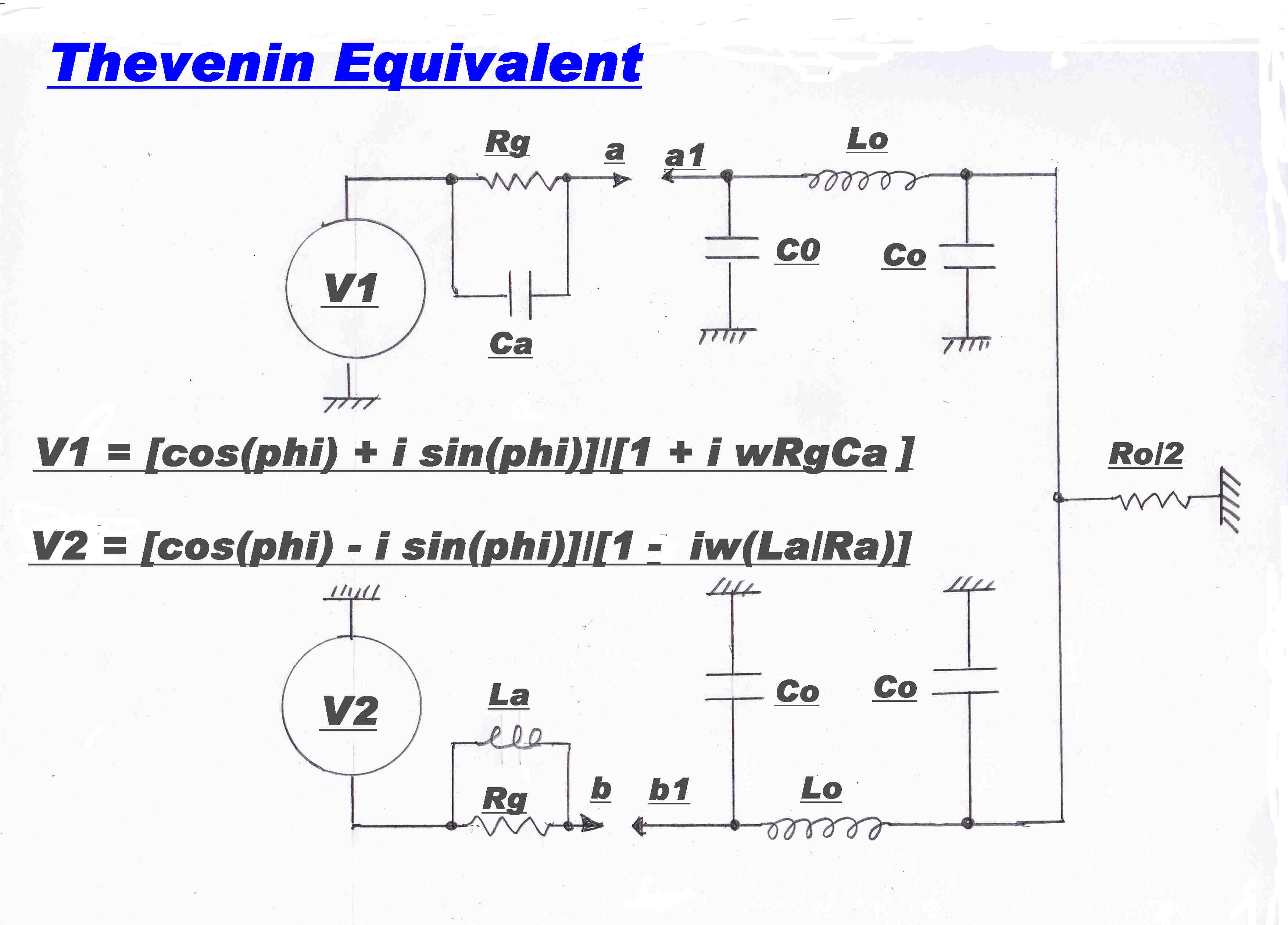 The Thevenin equivalent circuit is shown opposite.
Here the added capacity Co and inductance Lo are included with the generator to give a better intuitive understanding
of the output stage.
[1] The generator with the positive phase modulation V1 has its angle decreased by Δφ1
where: Δφ1 = tan-1( ω Rg Ca )
[1] The generator with the negative phase modulation V2 has its angle decreased by Δφ2
where: Δφ2 = - tan-1( ω ( La/Rg ) )
From the values of Ca and La derived above:-
| Δφ1| = |Δφ2|
The phase drive - or phase modulation - has been decreased, but the symmetry of the drive has been preserved.
The output impedance of the generator looking back from the terminal a and the input impedance of the PI network at a1
form a voltage divider.
This also changes the drive angle while preserving symmetry.
We get the very important result:-
The added components Rg Ca La maintain the symmetry of the phase drive while decreasing it.
A 90 degree phase drive no longer produces zero carrier output.
The phase deviation must be greater than 90 degrees to achieve zero carrier.

|
|
|
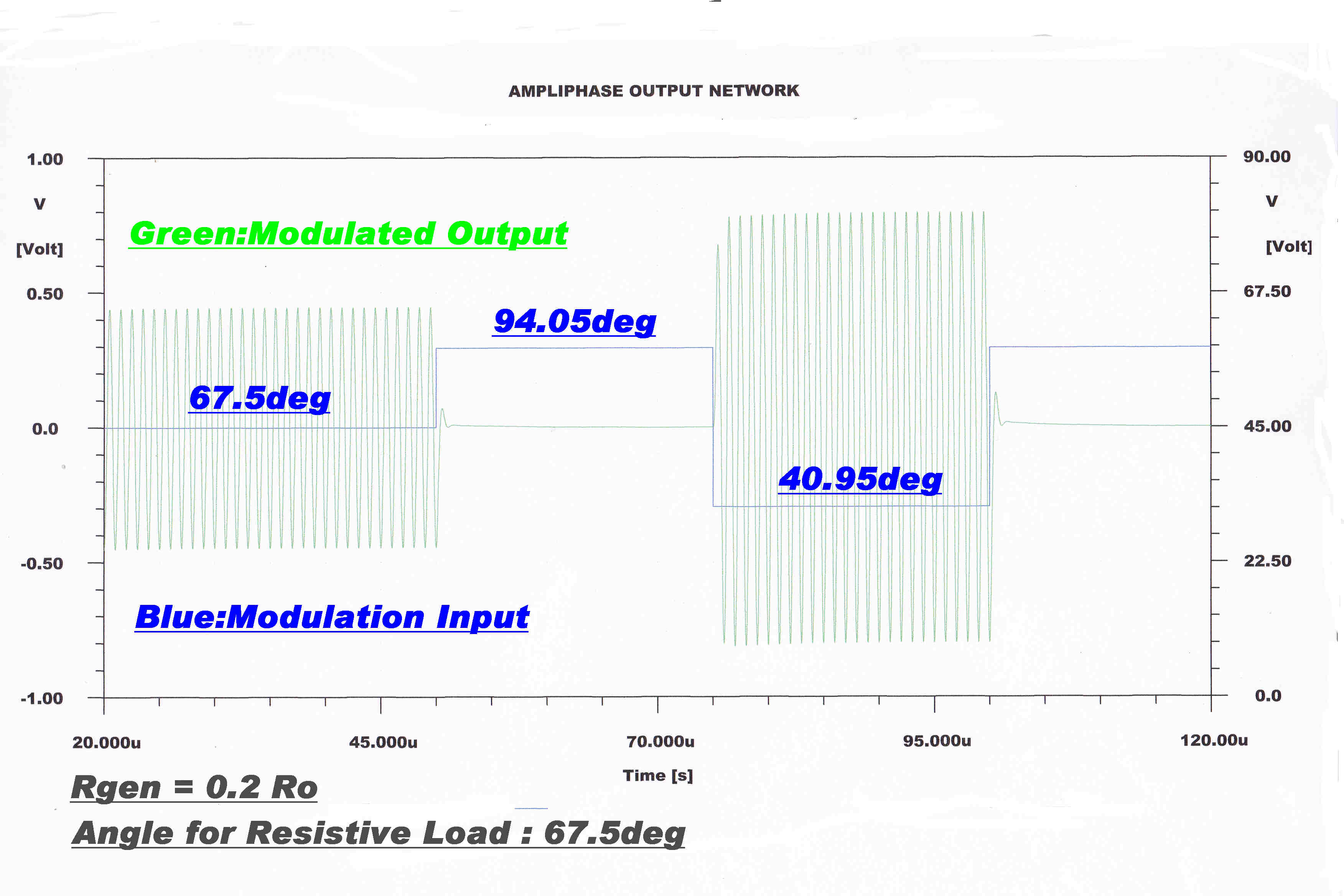
A computer solution for the Ampliphase network is shown. |
A computer solution for the Ampliphase network is shown. |
MORE COMPUTER SOLUTIONS FOR THE OUTPUT NETWORK
An important variable - the voltage on the plates of the output tube is included.
|
|
|
A computer solution for the Ampliphase network is shown. |
A computer solution for the Ampliphase network is shown. |
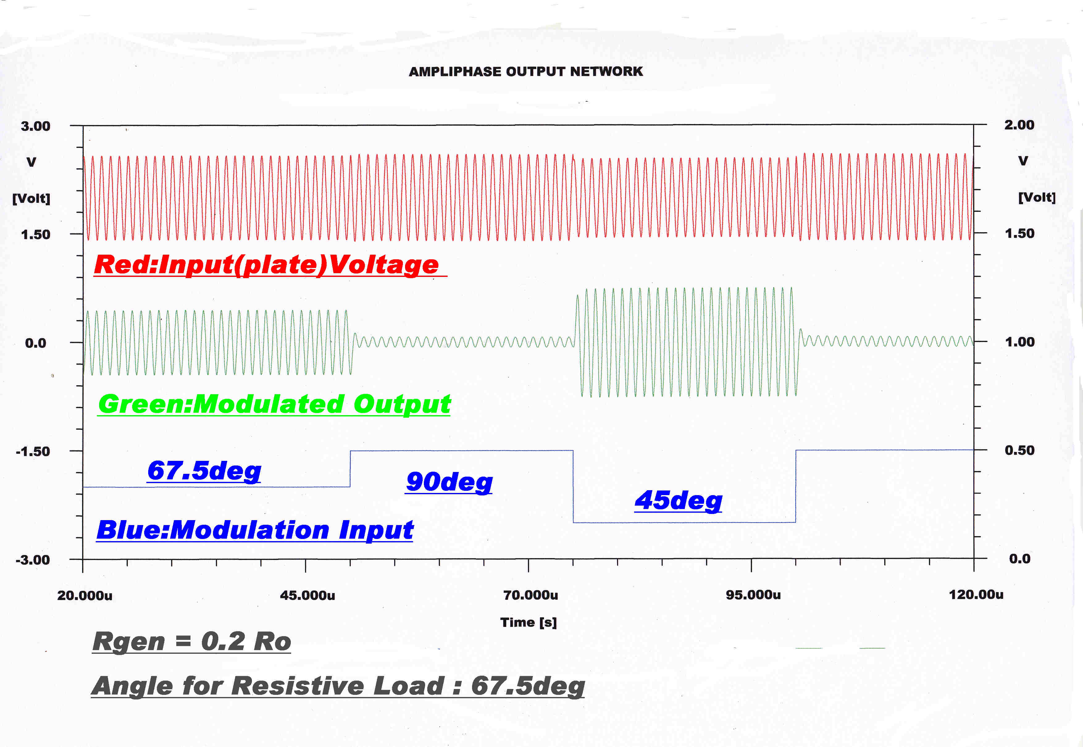
TRAPEZOIDAL PATTERNS FOR THE OPERATING CONDITIONS GIVEN ABOVE
|
|
|
A computer solution for the TRAPEZOIDAL PATTERN of the Ampliphase network is shown. |
A computer solution for the TRAPEZOIDAL PATTERN of the Ampliphase network is shown. |
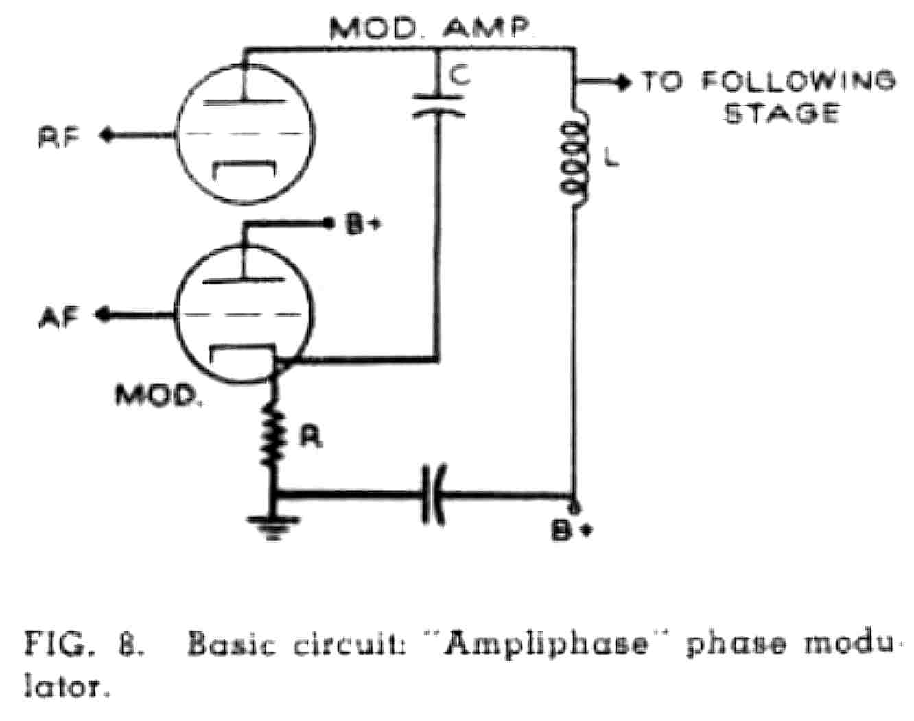
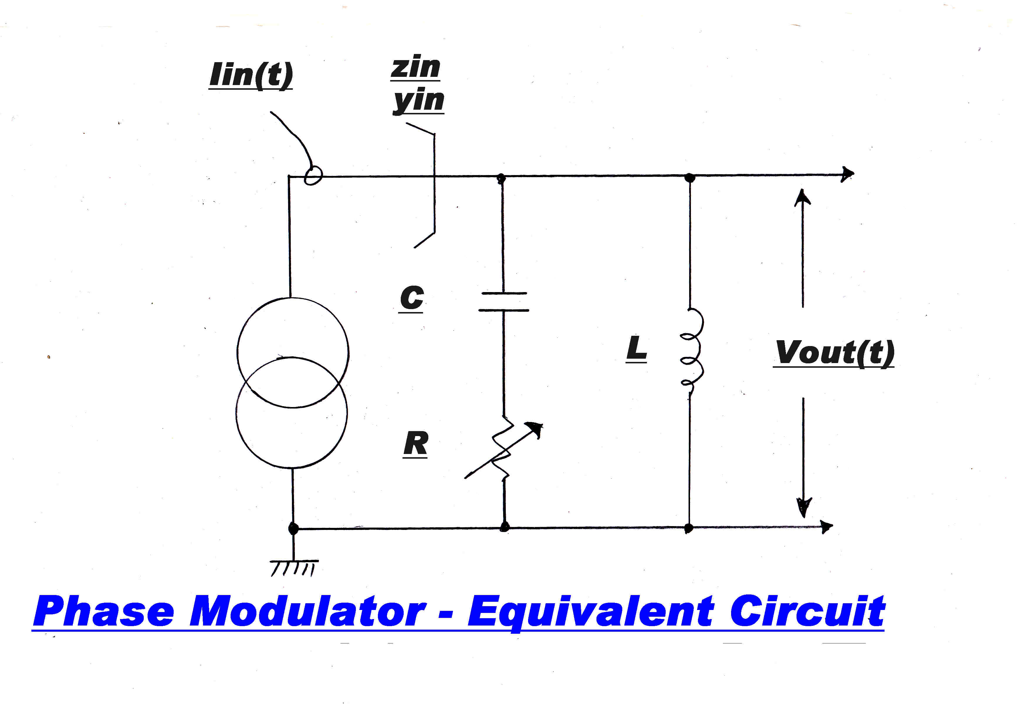 The basic circuit of the variable R phase modulator is shown on the right.
It comprises an LC tuned circuit driven by a sinusoidal current generator Iin(t)
of frequency fc.
The phase modulated sinusoidal voltage Vout(t) appears across the tuned circuit.
If R changes fron 0 to ∞, the phase of the output voltage can be made to change from -90 deg.
to +90 deg. with the correct dimensioning of the L-C network.
If R is infinite , all the current must flow in the inductor L and the phase change is + 90 deg.
If R is 0 we want the phase change to be - 90 degrees.
This can only happen if the tuned circuit is capacitive : the tuned circuit must resonate
at a frequency below fc.
Note:- Some modulators have the R in series with the inductor. Here the tuned circuit is
resonant above the frequency fc.
It will be shown later:-
(A) If the tuned circuit is resonant at fc/√2, then the amplitude of the output
is independent of R, that is it is free from amplitude modulation.
(B) That the relationship between the phase modulation φ and R is highly non-linear
and is given by:-
φ = tan-1[ 1/2 ( ωCR - 1/ωCR ) ] -----------------(1 )
where ω = 2 Π fc
(C) The R required for any given angle φ is also derived:-
R = [ 1/ω C][ tanφ + ( 1 + tan2φ )^( 0.5 ) ] -------------(2)
where -90 < φ < 90
These results are obtained by steady state analysis, so they are valid only for slow changes
in R. A numerical analysis for fast changes is given later on.
It turns out that the steady state analysis is valid for the conditions encountered in an
Ampliphase transmitter.
 The basic circuit used by RCA* in their early Ampliphase transmitters is shown opposite.
D R Musson RCA Broadcast News Vol. No. 119 Feb. 1964*
The upper tube represents the current source and the bottom tube represents the the
resistance R which is varied by the audio input.
For a linear modulation transfer characteristic, the resistance should vary according to the law
given in equation (2) above. This can be approxinated only over a very limited range by the
variation of input resistance into the cathode of the bottom triode with plate current.
The range is limited to about +(-) 8 degrees about 0 in the RCA modulator.
In general, I tend to shy away from any circuit design in which one non-linear law is
approximated by another entirely different law - difficult and questionable design!
The R in the cathode of the bottom triode is made large enough so that the cathode current
is a linear function of the audio on the grid.
We can now get a rough estimate of the variation of input resistance into the cathode
with cathode current.
Let the cathode current = IK : the cathode voltage = VK :
the incremental cathode resistanc RK
Then IK = k V3/2---- (three halves power law )
dIK/dVK = (3/2) k ( VK )1/2
Then: [ IK/k]1/3 = VK1/2
Which gives:-
RK = dVK/dIK =
(2/3) k-2/3 IK-1/3 ---------(3)
So the non-linear law in equation (3) is used as an approximation of the
non-linear law in equation(2) - not an enviable task for any design engineer!
The bottom tube is essentially a cathode follower with a capacitive load C.
The audio current in this capacitor must be small compared with the standing
cathode current.
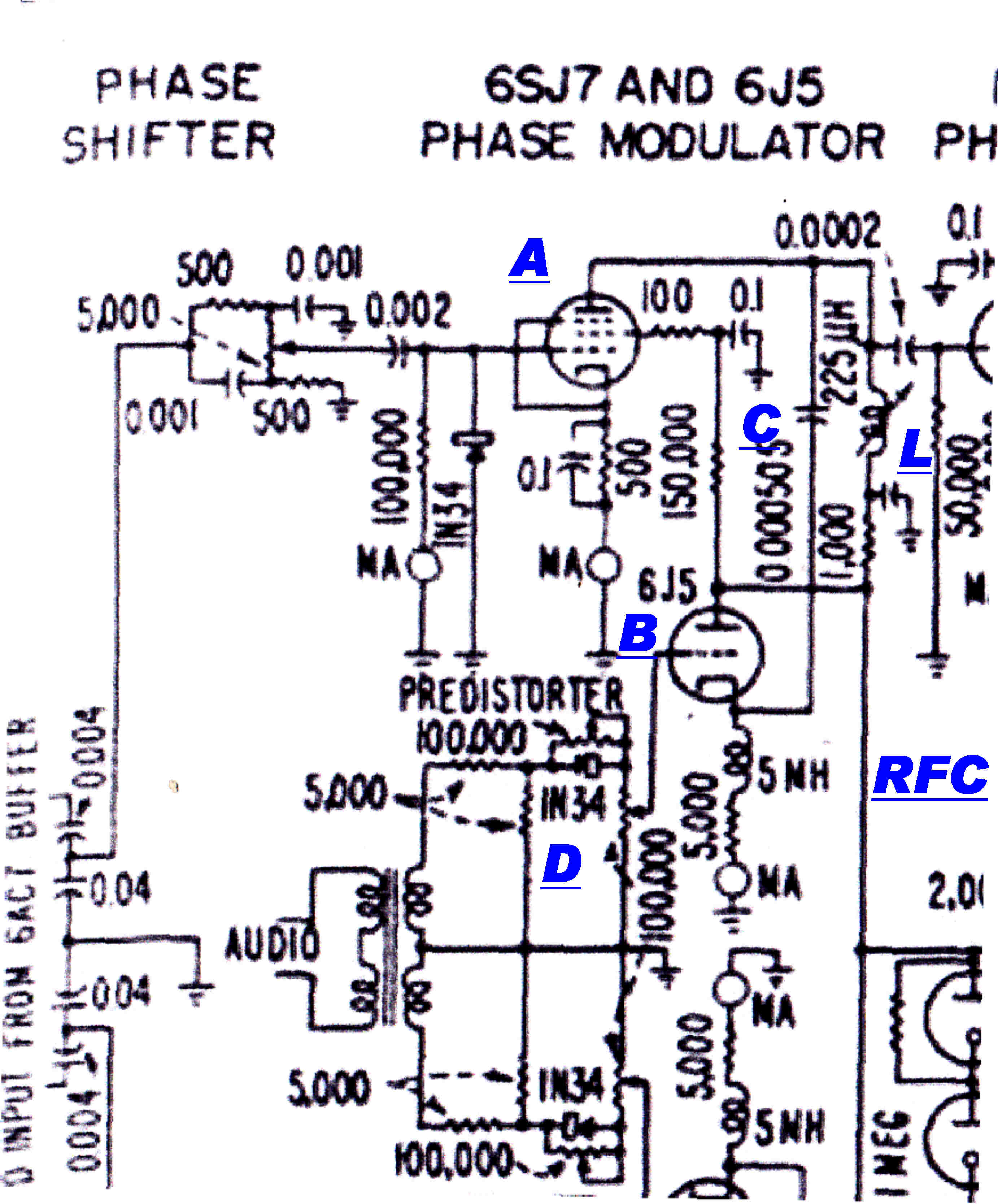 The phase modulator in the KFBK transmitter is shown on the right.
This transmitter preceeded the RCA dsesign.
The 6SJ7 (A) is the current source. The input resistance to the cathode of the 6J5 (B)
is the variable resistance.The resonant circuit is marked L and C.
The 5mH choke in the cathode of the 6J5 prevents the 5K cathode resistor from
shunting the cathode input resistance at carrier frequency, but is not large enough to
interfere with the variation of cathode current at audio frequencies.
f3db = 1/( 2 Π L/R )
= 1/( 2 Π 5 10-3/ 5 103 )
= 159KHz
The quiescent cathode current in the 6J5 is approx. 2.75Ma
The diode D gives an upward kink to the overall transfer characteristic to compensate
for the flatening at modulation peaks - so characteristic of ampliphase modulation.
Only one phase modulator is used to give a maximum phase shift of +(-) 8 deg.
The phase modulator is followed by a 6SJ7 frequency tripler to increase this to about
+(-) 22.5 deg. < br>
A steady state analysis of the phase modulator is now developed.
The transfer impedance Vout(p)/Iin(p) = z(p)
z(p) = [ ( R + 1/Cp )( Lp) ]/[ R + 1/Cp + Lp ]
= [ Lp + RCLp2] /[ 1 + RCp + LCp2 ]--------------(4)
For the steady state p = iω so :
z(i ω ) = [ - ω2RLC + iωL ]/[ 1 - ω2LC + iωRC ] ----------(5)
In other analysis it is easier to work with the transfer admittance which is:-
y(iω) = 1/z(iω) = [ 1 - ω2LC + iωRC ]/[ - ω2RLC + iωL ] ----------(6)
The amplitude of the carrier output is given by the modulus of z(iω) = |z(iω)|
If this is to stay constant and independent of R , then d|z|/dR = 0 and so d|y|/dR = 0
Also d( |y|2 )/dR = 0
Now from (6)
|y|2 = [ 1 + ω2R2C2 - 2ω2LC
+ ω4L2C2 ]/[ ω2L2
+ ω4R2L2C2 ]-------------(7)
Now d(x/z)/dy = (-x/z2)dz/dy + ( 1/z)dx/dy -----------------------(8)
If d(x/z) = 0 then (-x/z2)dz/dy + ( 1/z)dx/dy = 0
So x/z = (dx/dy)/(dz/dy) ---------------------(9)
Now using the numerator and denominator in equation (7)
Let x = [ 1 + ω2R2C2 - 2ω2LC
+ ω4L2C2 ] ------------------------(10)
y = [ ω2L2
+ ω4R2L2C2 ] --------------(11)
Then dx/dR = 2Rω2C2 and------------(12)
dz/dR = 2Rω4L2C2 ---------------(13)
Substituting back into equation(9)
[ 1 + ω2R2C2 - 2ω2LC
+ ω4L2C2 ]/[ ω2L2
+ ω4R2L2C2 ]
= 1/[ ω2L2 ] -----------------------------(14)
So [ 1 + ω2R2C2 - 2ω2LC
+ ω4L2C2 ] =
[ ω2L2
+ ω4R2L2C2 ]/
[ ω2L2 ] ----------------------(15)
Then ω2 = 21/2/LC
So ω = 21/2/[LC]1/2------------------------(16)
But ω = 2Πfc
where fc is the carrier frequency
So 2Πfc = 21/2/2Π[ LC ]1/2---------(17)
But 1/2Π[ LC ]1/2 = ft ---------------(18)
where ft is the resonant rfrequency of the LC tuned circuit
We then have
ft = fc / 21/2--------------------------(19)
That is: For no amplitude modulation, the LC circuit must be tuned down by 21/2
From above, the transfer impedance z( iω ) is given in equation (5) :-
z(i ω ) = [ - ω2RLC + iωL ]/[ 1 - ω2LC + iωRC ] ----------(5)
The phase modulation φ is the angle of this transfer impedance Ang[ z(i ω ) ]
φ = Ang[ z(i ω ) ] = tan-1[ ( ωL )/( - ω2RLC ) ]
- tan-1[ ( ωRC )/( 1 - ω2LC ) ] ----------------(20)
We have the identity:-
tan( a - b ) = [ tan(a) - tan(b) ]/[ 1 + tan(a)tan(b) ] so:
tan( Ang z ) = [ -ωL/ω2RLC - ωRC/( 1 - ω2LC )]/
[ 1 - ( ωL/( ω2RLC )) x ( ωRC/( 1 - ω2LC ) ) ] ---------(21)
The condition for no amplitude modulation derived above gave :-
ω2 = 21/2/LC
Substuting this in (21) we get:-
tan( Ang z ) = [1/2][ ωCR - 1/ωCR ] -----------------------(22)
The resistance Ro for zero phase change is then given by:
Ro = 1/ωC ---------------(23)
The function of R to give linear phase modulation from -90deg to +90deg is now derived.
If we multiply tan( Ang z ) = [1/2][ ωCR - 1/ωCR ] by ωCR we get the quadratic equation in R :-
ω2C2 R2 -2 ωC tan(φ) R - 1 = 0 --------------------(23)
The solution is:-
R = [ 1/ωC] [ tan(φ) + ( 1 + tan(φ)2)1/2 ] -----------------(24)
The input resistance into the cathode of a triode given above (equation 3) is a poor approximation to this law.
This limits the useful modulation range to about +(-) 8 degrees.
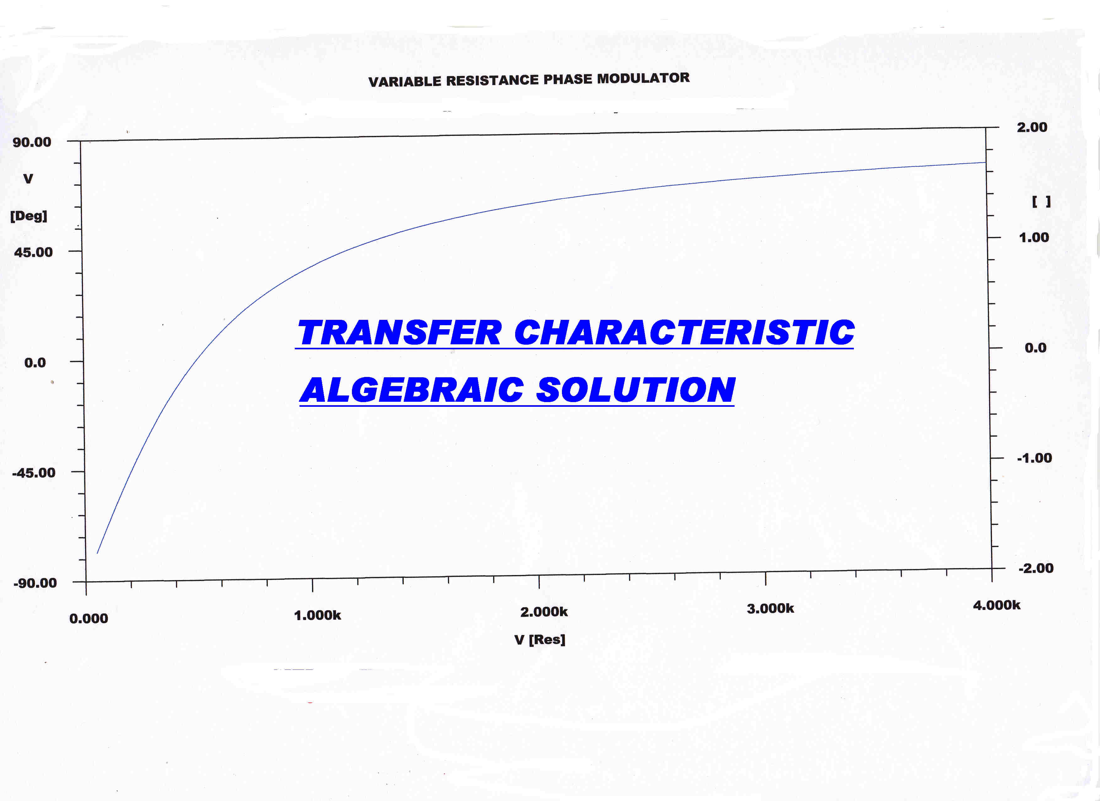
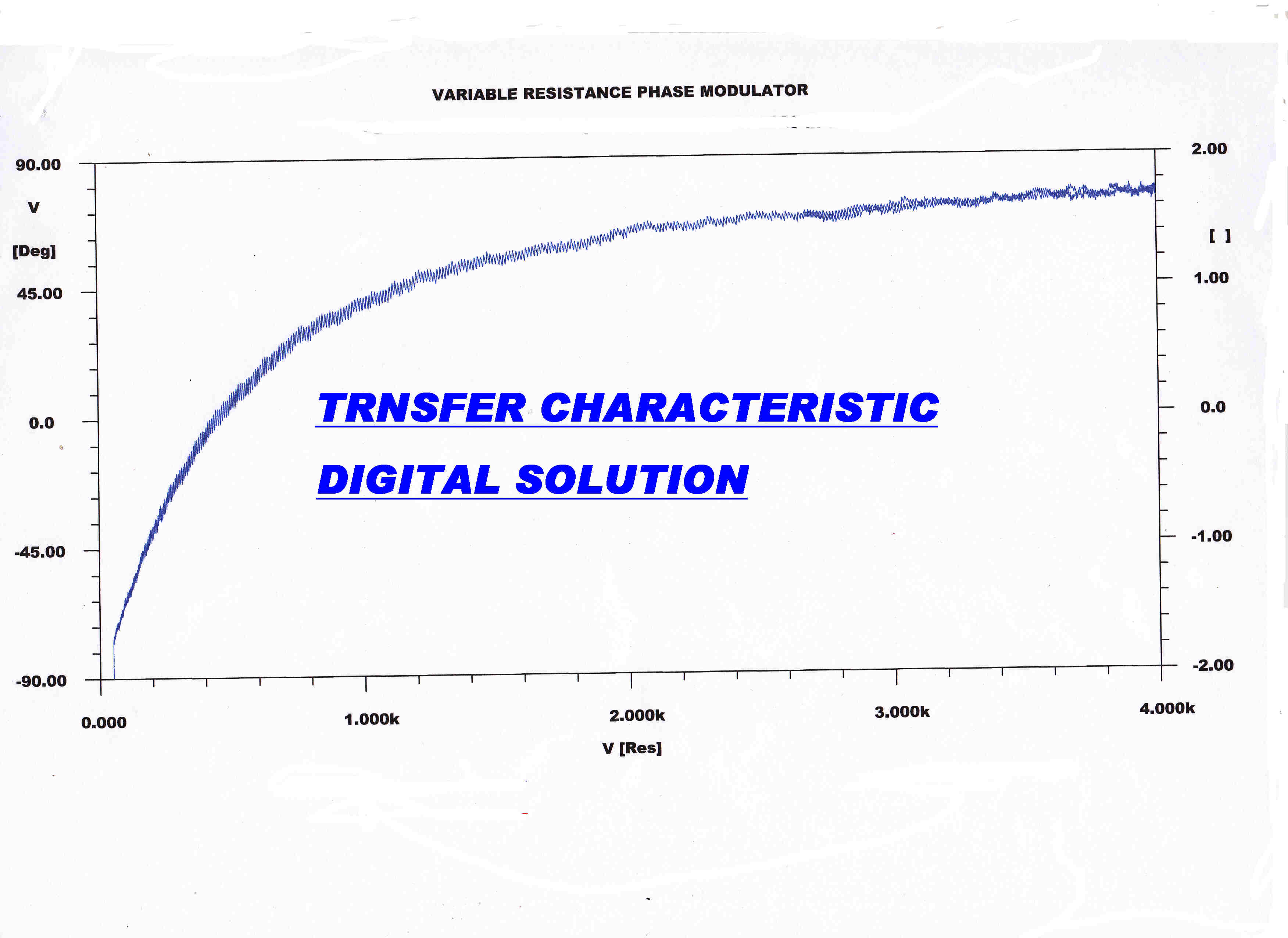
A plot of the transfer characteristic ( equation 22 ) together with a direct digital solution of the phase modulator circuit is given below.
|
|
|
A plot of the transfer characteristic - phase angle φ versus R - according to the equation:- |
A direct digital solution of the modulator circuit independent of the algebraic equation. |
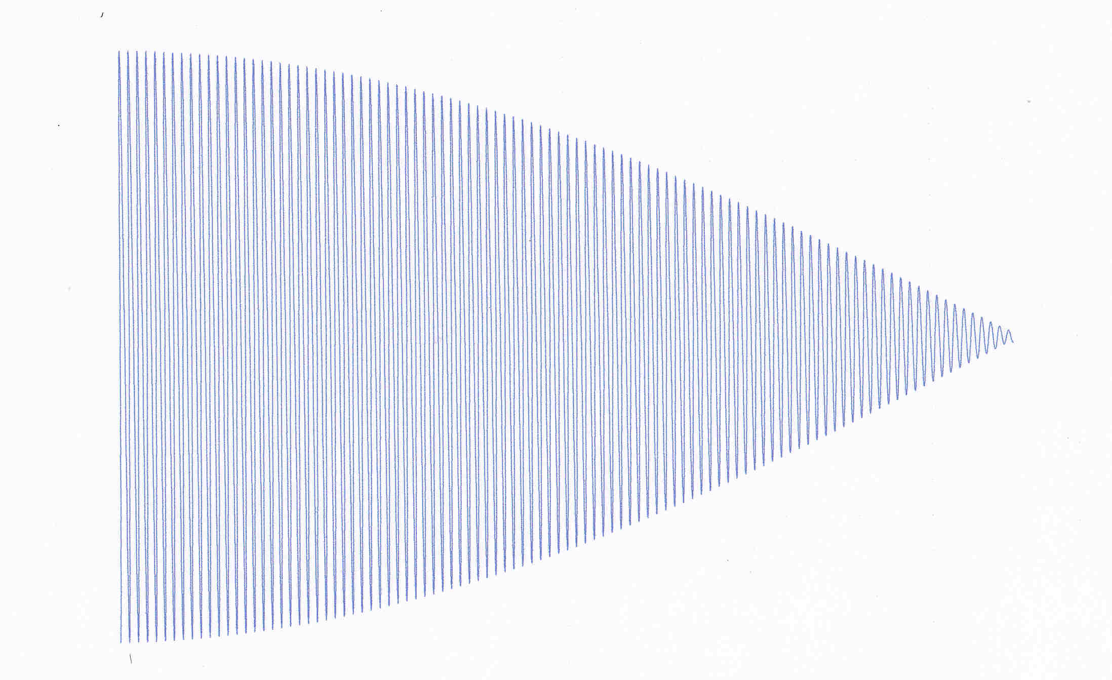
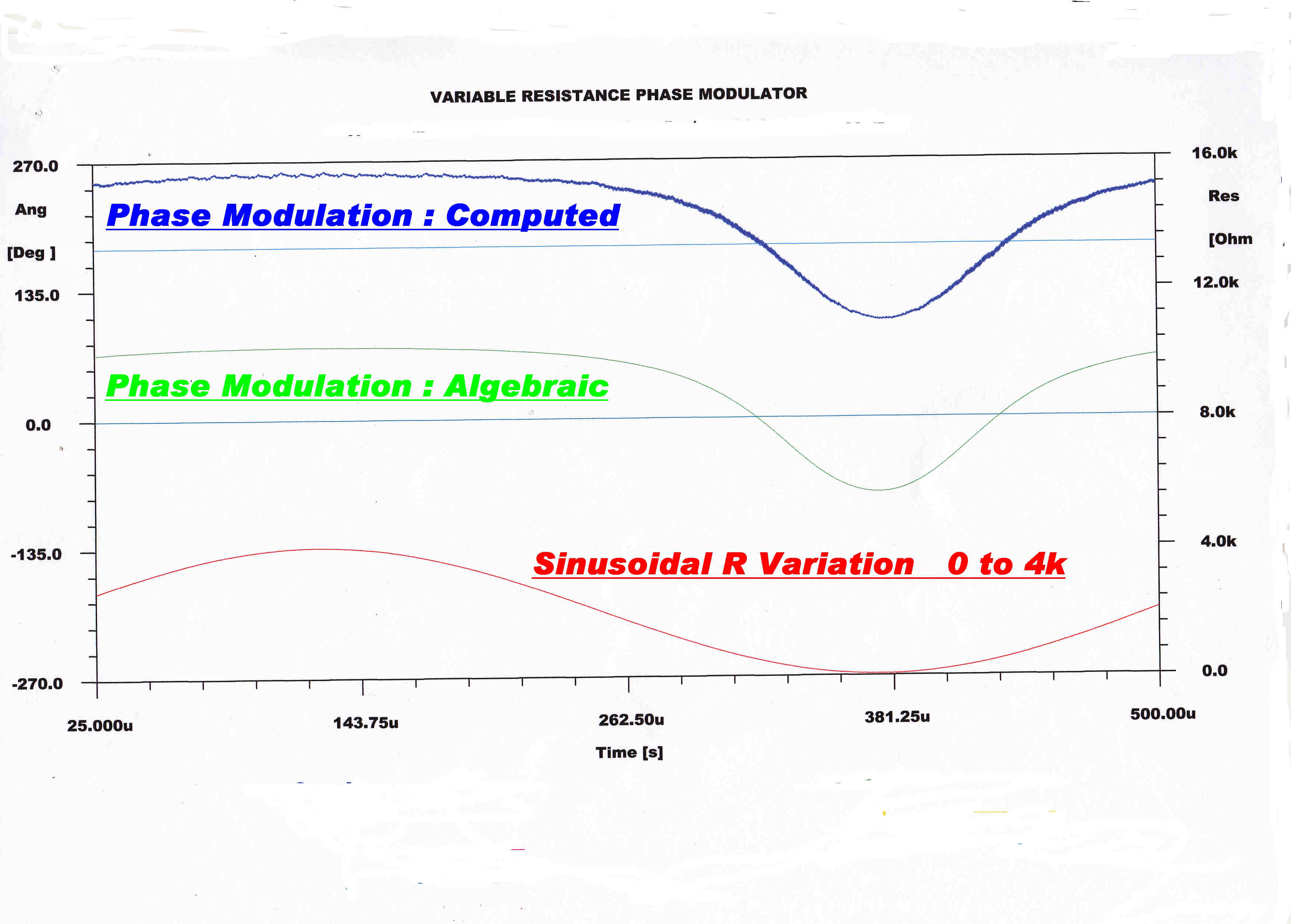 The output from the phase modulator for a sinusoidal input illustrating the extreme non-linearity.
The resistance R is varied in a linear manner fom 0 to 4Kohms.
The algebraic solution is developed with steady state equations.
It is valid only for slow input changes.
A time variable circuit element [ R - L - C] in a network invariably throws up a non- linear differential equation
which cannot be solved by classical methods.
Numerical methods on a digital computer overcome the problem.
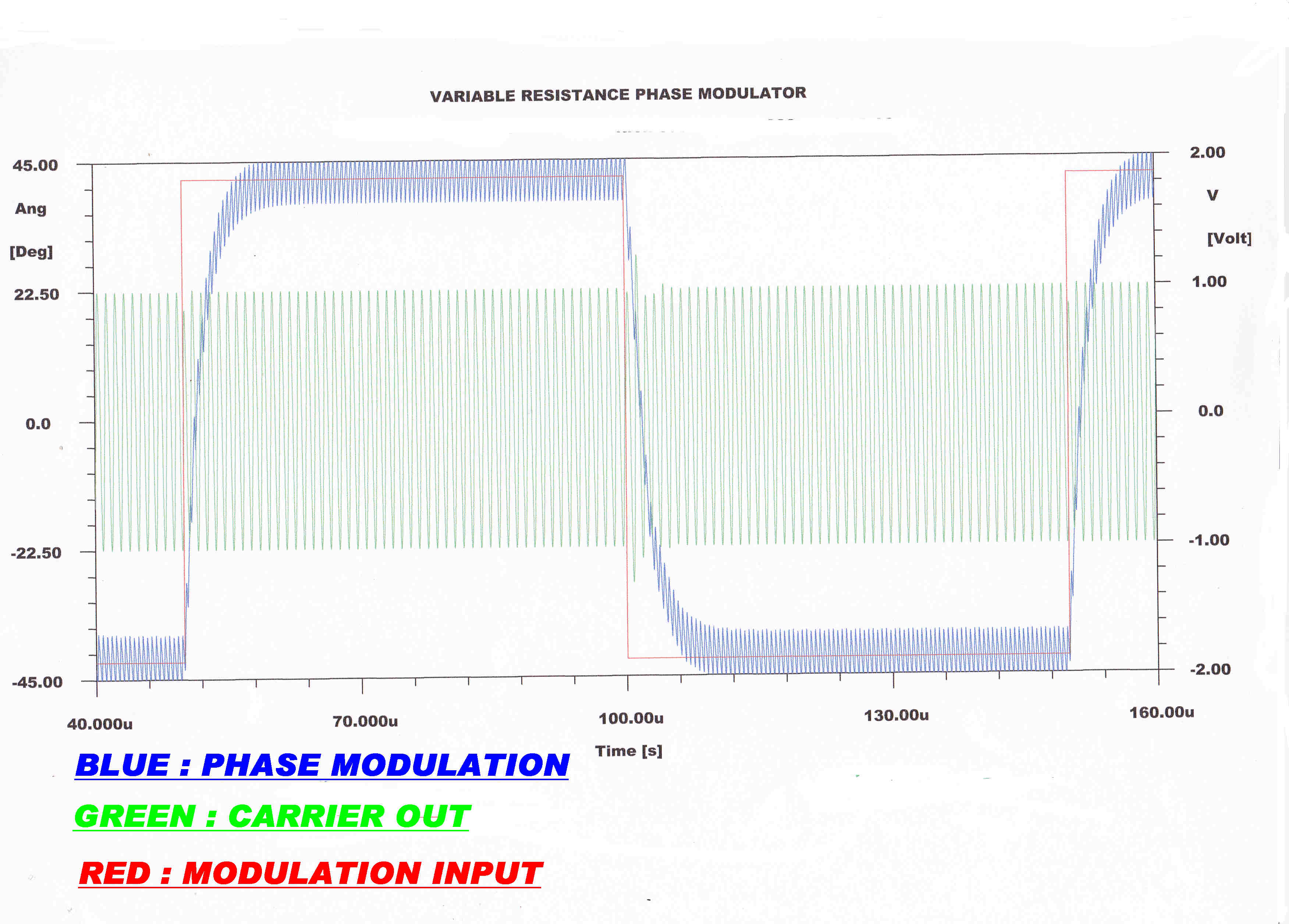
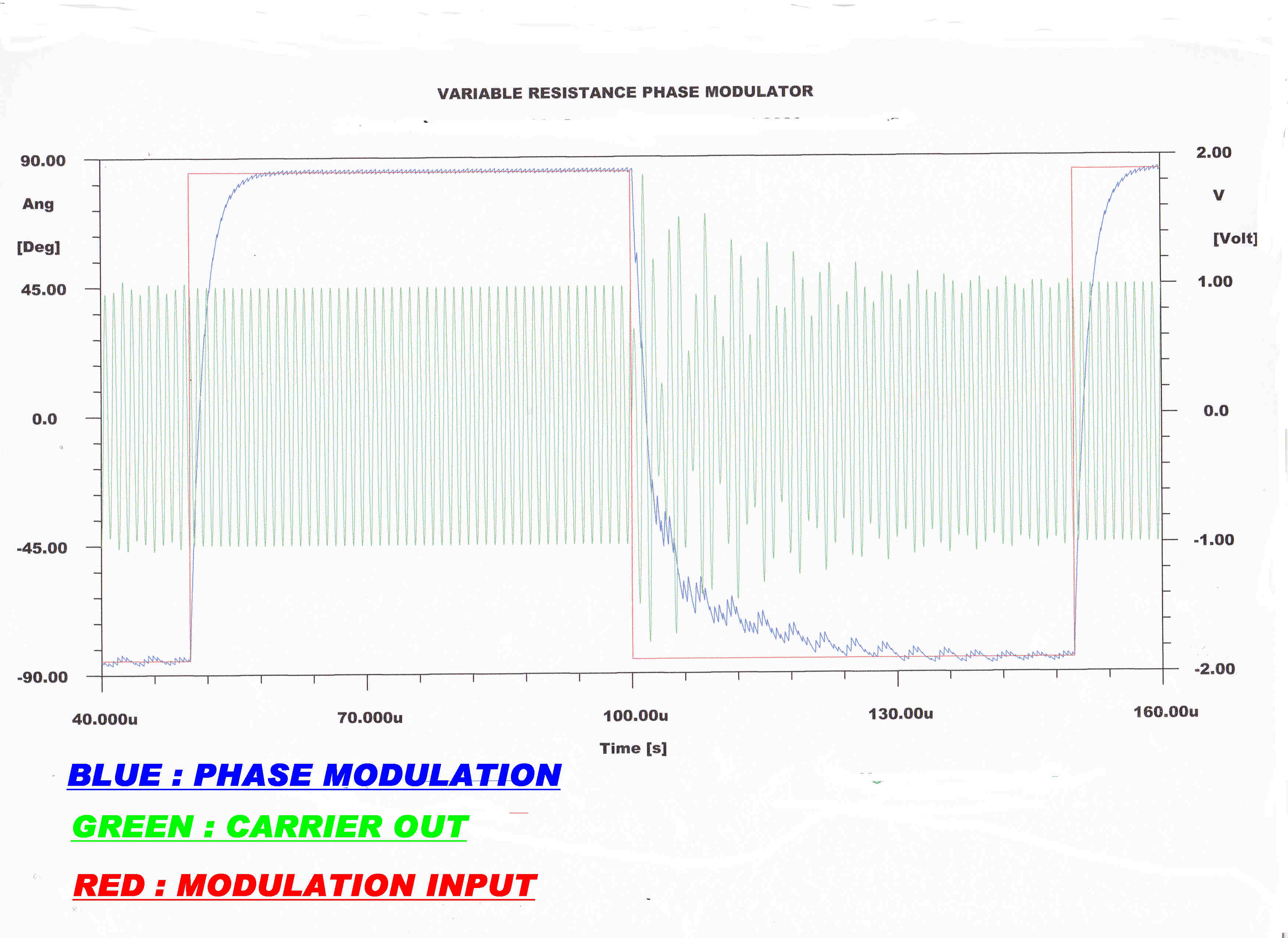
The complete solution of the transient response or step inputs is given below.
It is shown that transients do appear for fast (step) inputs.
Fortunately, these are outside the range encountered with an audio input to the modulator and the
steady state analysis can be used in design.
|
|
|
A step function is the fastest input available, but transients only start to develop
with modulation between +43 degrees. and - 43 degrees. |
Modulation is now between +88 degrees and -88 degrees. |