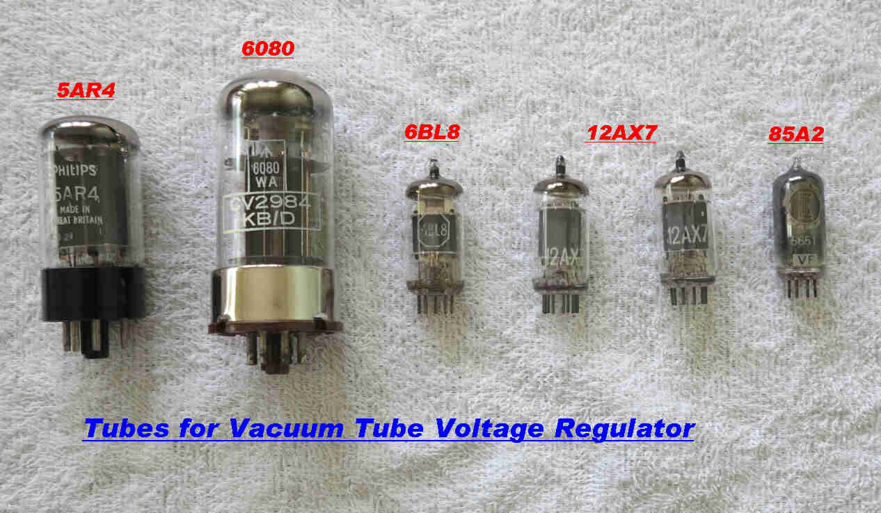
VACUUM TUBE VOLTAGE REGULATOR
CONTACT : COMMENTS AND QUESTIONS
back/home
This voltage regulator is designed to provide the 300 volt high tension for the low level
stages of a vacuum tube audio system.
The low level stages consist of:-
(1) A high gain low noise pre-amplifier for a magnetic pickup.
(2) A mixer stage in which the channels can be added or subtracted to make the system
responsive to lateral or hill and dale recordings.
The relative gains of the channels can be changed to give excellent cancellation
of the response which is not required.
(3) A universal disc equaliser.
(4) A universal tone control.
(5) An output amplifier to drive a long length of 75 ohm coax cable between the low level
audio stages and the power amplifier.
The cable operates into a high impedance at the receiving end and is driven
from the characteristic impedance at the sending end.
It is generally agreed that test equipment requires regulated high tension
to achieve stability and accuracy.
A good case can be made for highly regulated high tension supplies for high
performance low level audio stages.
The maximum gain of the pre-amplifier is 47 db.
The RIAA bass equalisation requires a 6db/octave slope between 500 Hz
and 50 Hz -- adding another 20 db of gain at low frequencies.
The universal tone control can add an extra 20 db of boost at 50 Hz
- giving a total gain at 50Hz of 87db.
The low level stages are designed to be flat down to 10 Hz,
so, in reality, this gain extends down to a few Hz.
To reduce the 100Hz on the HT rail at least two stages of LC filtering are required.
This filter is not terminated by the output resistance of the rectifier.
This results in:-
(1) Peaks in the output impedance at frequencies below 100 Hz.
These introduce spurious coupling between stages which modify the overall
response and may lead to instability.
(2) Peaks in the response of the filter at frequencies below 100Hz.
Slow speed changes in mains voltage appear on the rectifier output.
These can be amplified by peaks in the filter response.
If passed on to the low level stage of a power amplifier they can cause
serious overloading.
If the power amplifier is DC coupled, large slow speed excursions of the
speaker cone result.
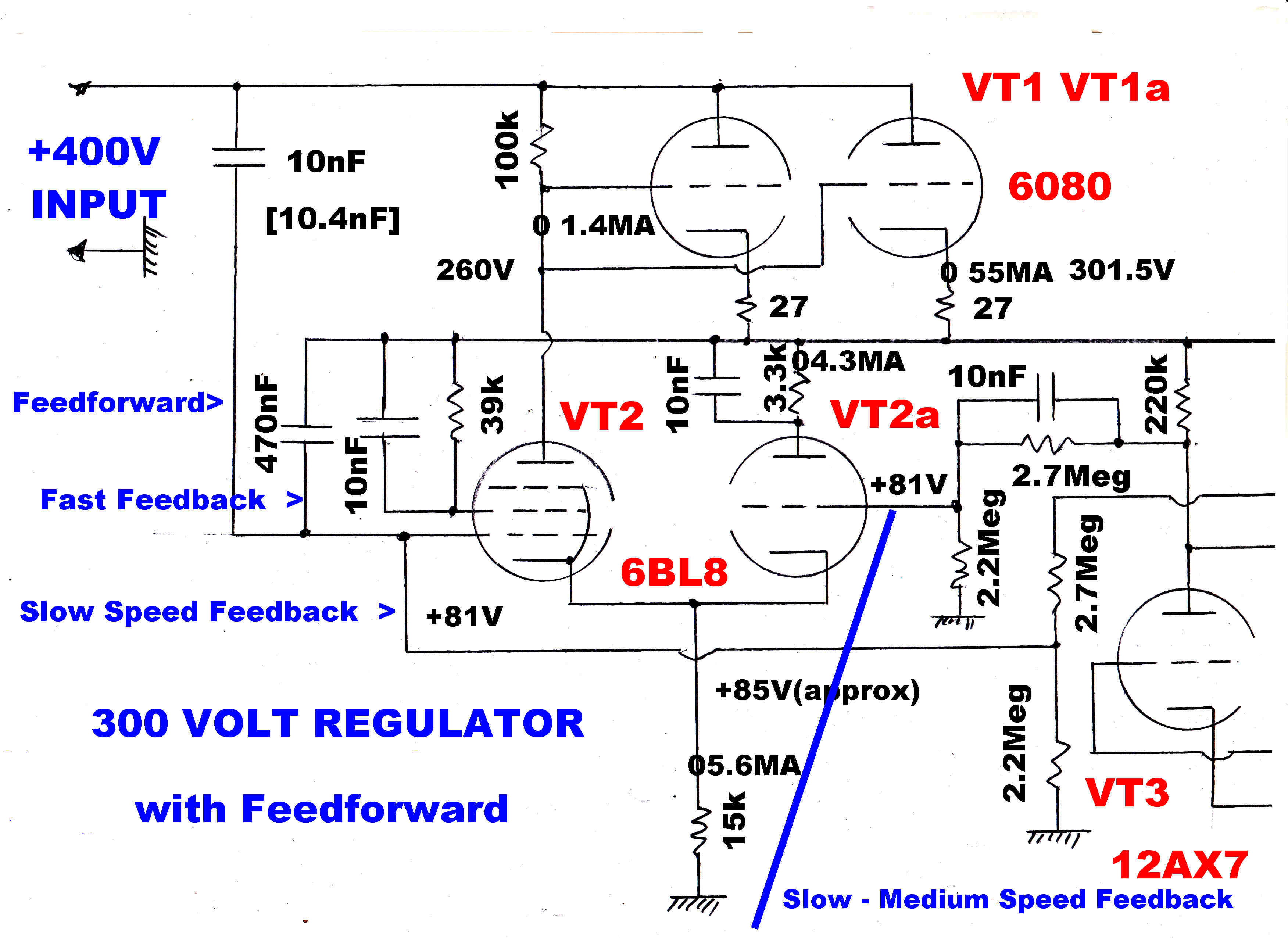
The block diagram of the regulator is shown below:-

[A] It is imperative that the ouput impedance remain low at high frequencies.
This dictates the presence of a large capacitor in parallel with the output
of the regulator.
Most amplifiers have a large bypass capacitor on the high tension rail,
so this capacitor would appear anyway when the regulator is connected to the load.
Together with the output resistance of the regulator pass tube, this capacitor
produces a dominant pole on the negative real axis in the feedback loop transfer function.
The output resistance of the pass tube is 88.1 ohms. The output capacitor is 22uF.
Together they form a time constant of 1.938mS - giving a pole on the negative
real axis at 82.1 rad/sec.
[B] To achieve low frequency output impedance in the milli-ohm range, the DC
loop gain must be of the order of 104.
This implies at least three stages of DC amplification.
Each stage introduces at least one extra pole into the loop giving rise to
dynamic stability problems.
The solution is to use two feedback loops in parallel:-
A DC to medium speed high gain loop and a high frequency low gain loop.
The final amplifier stage has two inputs:-
One from the high gain DC coupled amplifier and another taken directly
from the output.
The level of both inputs is equal at about 3KHz, and above this the high
speed loop dominates and determines the overall stability of the system.
Comparison with the gas tube voltage reference is made at the input of
the DC amplifier, so this amplifier uniquely determines the DC voltage output.
The HF loop is AC coupled.
The turnover frequency is determined by the 480.4 ( 470 + 10.4 )nF capacitor and the
1.2Meg driving resistor to give a time constant of 0.576S and a frequency of 0.276Hz.
[C] The two stage DC coupled amplifier has a total DC gain of 292 and a turnover
frequency of about 20Hz.
Unity gain is at about 2.5KHz with a phase change of 90 degrees.
Above about 3KHz the response of the high frequency loop begins to dominate
and uniquely determine the stability of the regulator.
The output stage has a gain of 64.7.
The total DC gain is therefore 292x64.7 = 18,892 (85.5db).
The pentode output capacity, the input capacity of the pass tube and stray C form
a second pole in the high frequency loop with a time constant 3.945 usec
to give a pole at - 2.532x10⁵ rad/sec.
Notice the other pole in the HF loop is at 82.1 rad/sec.
The difference in magnitude is important and leads to stability.
Further capacitive loading across the output pushes the 82.1 rad/sec pole
towards the origin. It will be shown later that this increases the stability margin.
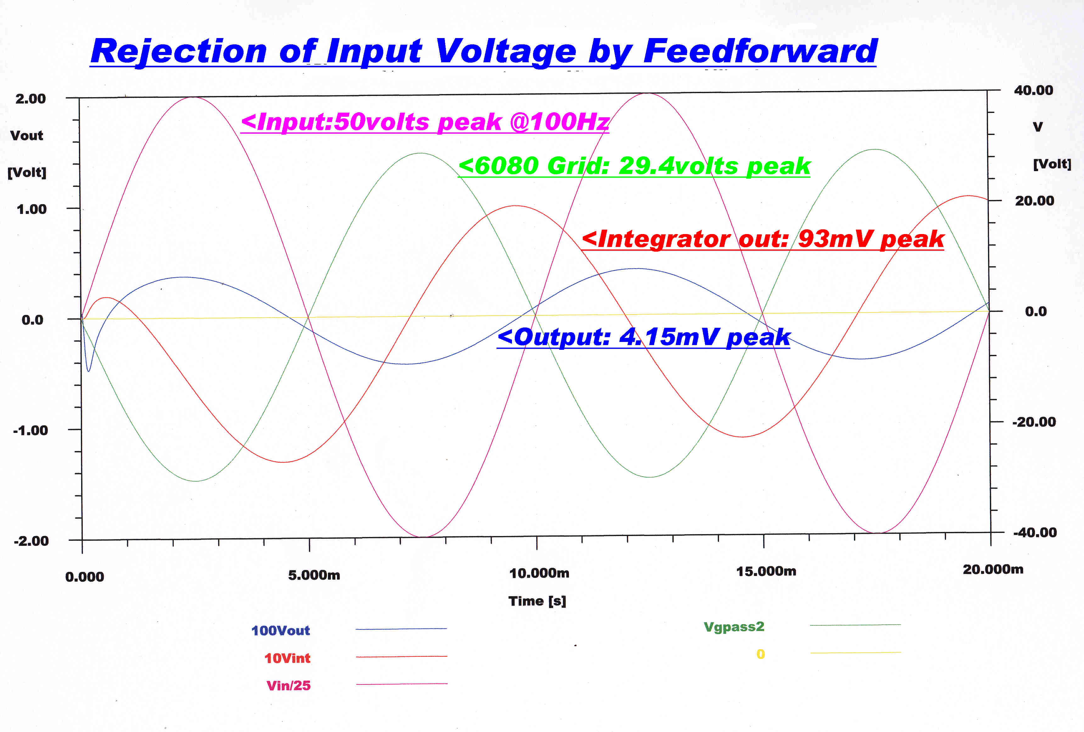
[D] It is possible to use feedforward to reduce the level of hum
and slow speed mains transients on the regulator output.
Suppose the rectifier has a 50 volt peak ripple output at 100 Hz.
Since the pass tube triode has a low μ of 1.7, a voltage of 50/1.7 ( 29.4V)
is required on the grid to suppress this input.
At 100 Hz the gain of the DC coupled amplifier is 26db (20) and the gain of
the high frequency amplifier is 64.7 to give a total gain of 1294.
This means that 29.4/1294 (22.7mV) must appear on the output.
The 29.4V grid voltage on the pass tube can be provided by feeding
an attenuated version of the input into the the grid of the high frequency
amplifier - feedforward.
Virtually no 100 Hz ripple then appears on the output.
The attenuator formed by the 10.4 and 470nF capacitors gives the correct
loop gain for feedforward cancellation.
The complete circuit of the regulator is shown below:
|

|
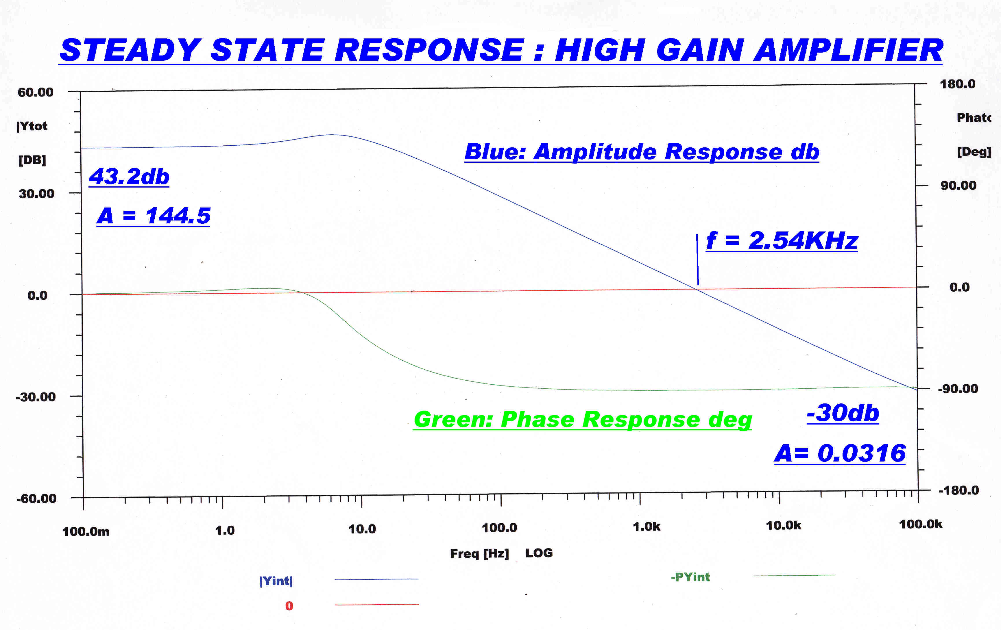 The response of the high gain DC coupled amplifier is shown on the right.
The amplifier consists of two cathode coupled 12AX7 stages.
The usual name for such a stage was "long tailed pair" - probably because
the common cathode resistor looked like a tail attached to the two triodes.
The input stage acts as a differential amplifier, comparing the output voltage
divided down in the resistive divider with the 83 volt reference.
Since any grid current will develop a spurious voltage in the divider, it is
important to keep this as low as possible.
The grid current has two main components:-
(1)Fast thermionic electrons on the tail of the Maxwell distribution
intercepted by the grid.
(2) Positive ions produced by residual gas in the tube.
The quiescent plate current (0.5Ma) and plate voltage (100V) are chosen to give
a grid bias of -1volt. This is high enough to repell virtually all fast emitted
electrons from the grid.
In a well made tube the ion grid current is usually well below 1nA. The driving
point reasistance to the grid is 71k // 187k to give 51.5k. Any spurious voltage
would then be below 50 uvolts.
An RC low pass filter is placed between the gas tube and the other grid to
filter out noise. The output resistance of this is 56k, comparable with the
divider output resistance, to give balance.
The response of the DC coupled 12AX7 high gain amplifier should
fall off at 6db/octave, so the single stage high frequency loop
can predominate at high frequencies.
The 6db/octave slope is generated by the 330pF feedback resistor.
To ensure loop stability:-
[1] A 17db shelf is produced by the 15k resistors and
2.7nF capacitor between the plates of the first stage.
[2] The top resistors of the coupling dividers are bypassed
by 10nF capacitors.
Left unbypassed, the output capacity and input capacity produce
two poles on the real axis in the forward path.
The bypass capacitors combine the capacities to produce
a single pole and so inprove overall stability.
Input Stage
|
|
|
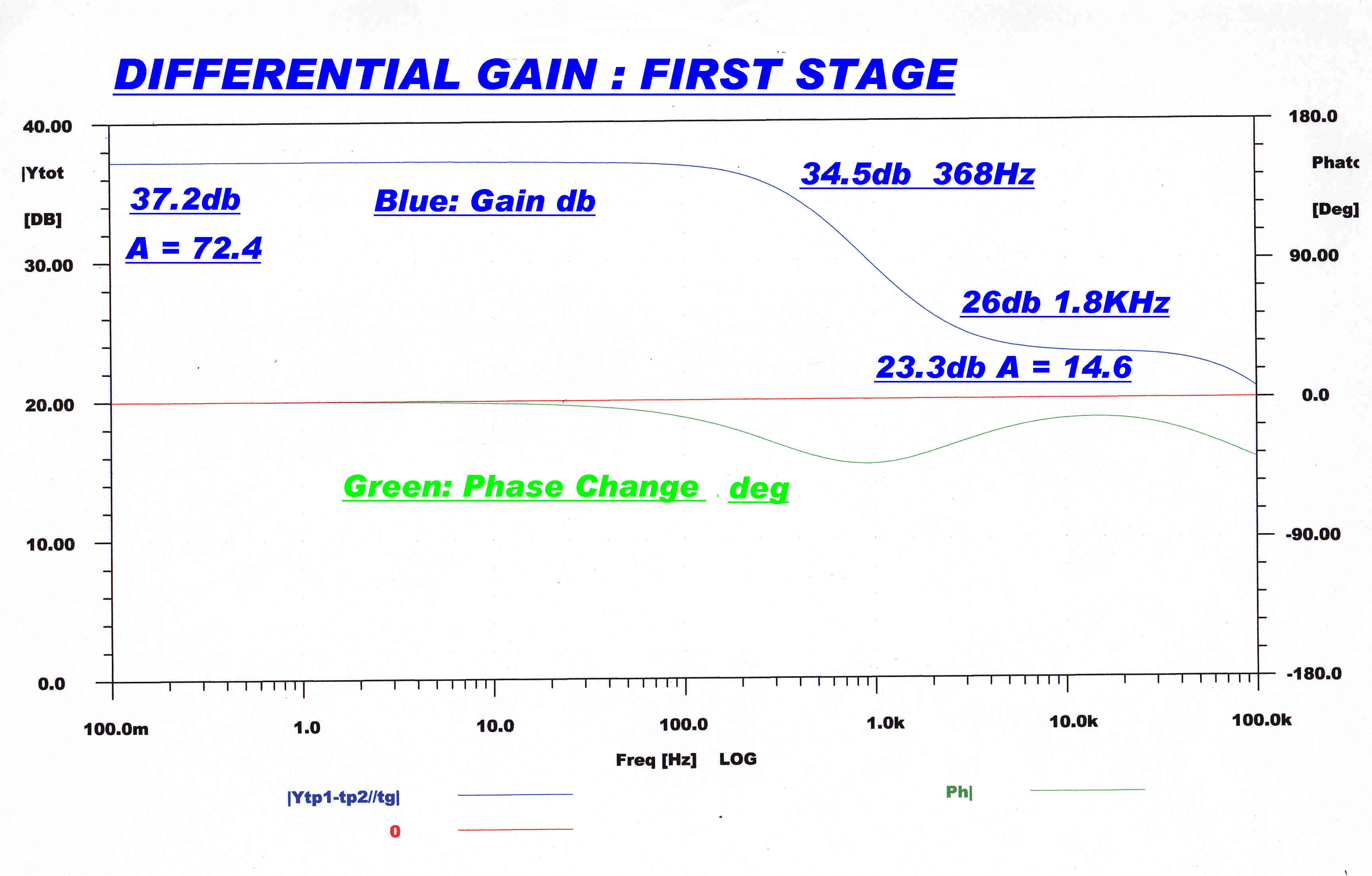
Differential Gain - Plates of First Stage |
Differential Gain - Grids of Second Stage |
 The high frequency feedback loop consists of the cathode coupled 6BL8
triode pentode and the 6080 pass tube cathode follower.
The high frequency feedback loop consists of the cathode coupled 6BL8
triode pentode and the 6080 pass tube cathode follower.
The equivalent circuit is shown on the right.
The cathode follower pass tube acts like a voltage generator:-
Vout = Vin[ μ/( 1 + μ ) ]
with an output resistance given by :-
Ro = [ 1/Gm ][ μ/( 1 + μ ) ]
For the 6080 μ = 1.7
For the two triodes in parallel: Gm = 8.4Ma/V
So:
Vout = 0.63Vin
Ro = 74.95 ohms
The grid of the 6BL8 triode is held at earth potential at high frequencies.
For frequencies above about 3Hz the pentode grid is driven directly from the
output via the 470nF capacitor.
The triode cathode resistance produces cathode degeneration in the pentode.
The effective Gm of the pentode ( Gma ) is given by :-
Gma = Gmgp/( 1 + Gmgk Rk )
where:-
Gmgp is the grid plate Gm of the pentode
Gmgk is the grid cathode Gm of the pentode
Rk is the cathode resistor
From above:-
Rk = [ 1/Gmt ][ μ/( 1 + μ ) ]
Substituting:-
Gma = Gmgp/[ 1 + ( Gmgk/Gmt )μ/( 1 + μ )]
So: Gma = 0.647 Ma/V
The total output resistance Rtot looking into the cathode of the 6080 pass tube is:-
Rtot = 74.95 + 13.5 = 88.5 ohms
Together with the 22uF output capacity, this forms a pole on the negative real axis
of time constant 1.946mS - 513.6 rad/sec - 81.8Hz.
The output capacity of the pentode, the input capacity of the pass tube and stray C
add to 39.5pF. Together with the 100k load, these form a pole on the negative real axis
of time constant 3.95uS - 2.53x10⁵ rad/sec - 40.29Hz.
The loop gain Atot is given by:-
Atot = 0.647x10⁻³ 105 x 0.63
Atot = 40.8
Bypass capacitors on equipment high tension rails will appear in parallel
with the 22uF output capacitor.
It will now be shown that this increases the stability of the HF loop.
As shown above, the forward transfer function Yf(p) for the loop
has the form :-
Yf(p) = A/( 1 + τ1p )( 1 + τ2p )
The closed loop transfer function Yc(p) = μ/( 1 + μβ )
where:
μ = A/( 1 + τ1p )( 1 + τ2p )
β = 1 ( via the 470nF capacitor. )
Substitution yields the denominator D(p) in the closed loop Yc(p) as:-
D(p) = 1 + [ (τ1 + τ2 )/( 1 + A ) ] p
+ [ (τ1 τ2 )/( 1 + A ) ] p2
The standard form of the second order transfer function for analysis is:-
Y(p) = 1 / ( 1 + 2ζτ p + τ2 p 2 )
where ζ is the dampimg factor
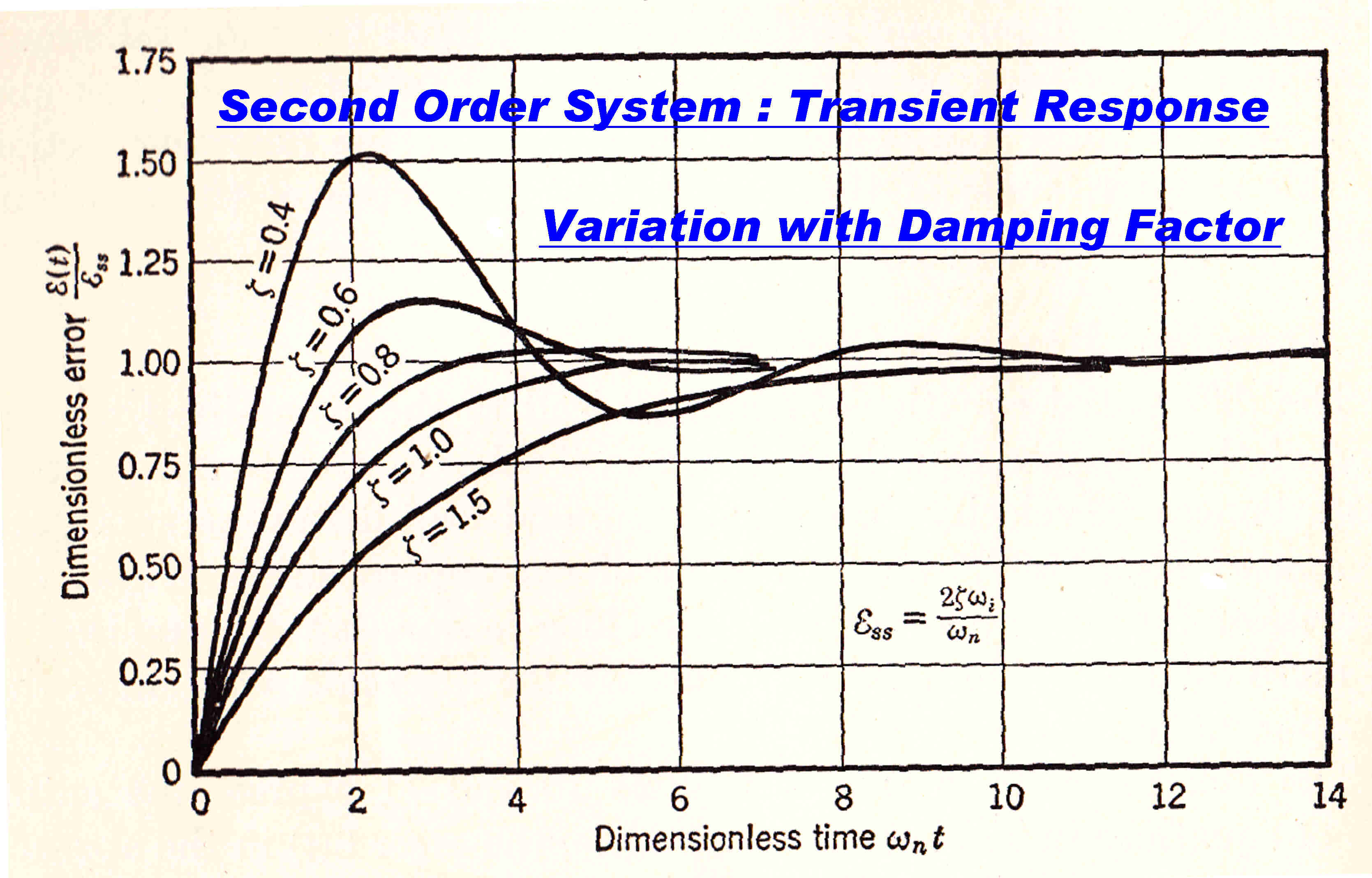 The response of a second order system for various damping factors is shown opposite:
For damping factors less than 0.707, the system will ring at a frequency
ωo -- where ωo = 1/τ
The denominator D(p) is now rearranged in standard form:-
D(p) = 1 + 2{ (1/2)( 1/( 1 + A)1/2 )( (τ1/τ2)1/2
+ (τ2/τ1)1/2 ) }
{τ1τ2/( 1 + A ) }1/2 p
+ {(τ1τ2/( 1 + A ) )1/2 }2 p2
So that now ζ = { (1/2)( 1/( 1 + A)1/2 )( (τ1/τ2)
1/2 + (τ2/τ1)1/2 ) }
And τ = (τ1τ2/( 1 + A ) )1/2
The ringing frequency ωo = 1/τ =
( ( 1 + A )/ τ1τ2 )1/2
The value of ζ gives a measure of loop stability:-
[1] ζ = K [ 1/( 1 + A ) ]
[2] ζ = K ( (τ1/τ2)
1/2 + (τ2/τ1)1/2 )
so the stability increases as the ratio of pole separation increases.
Adding extra capacity to the 22uF output capacitor by external loading brings the lower pole
further in towards the origin, increases the ratio, and so improves the loop stability.
NUMERICAL VALUES
Now evaluate the value for ζ for the loaded and unloaded cases:-
Remembering:-
ζ = { (1/2)( 1/( 1 + A)1/2 )( (τ1/τ2)
1/2 + (τ2/τ1)1/2 ) }
No External C Load:-
C = 22uF : τ2 = RC = 88.1x22x10-6 = 1.9382x10⁻³
τ1 = 3.945x10⁻⁶ :: A = 64.7
ζ = 1.369 : so there is no overshoot or ringing.
With 44uF external load capacity:
τ2 = RC = 88.1x66x10-6 = 5.815x10⁻³
ζ = 2.369 : so the stability has been improved
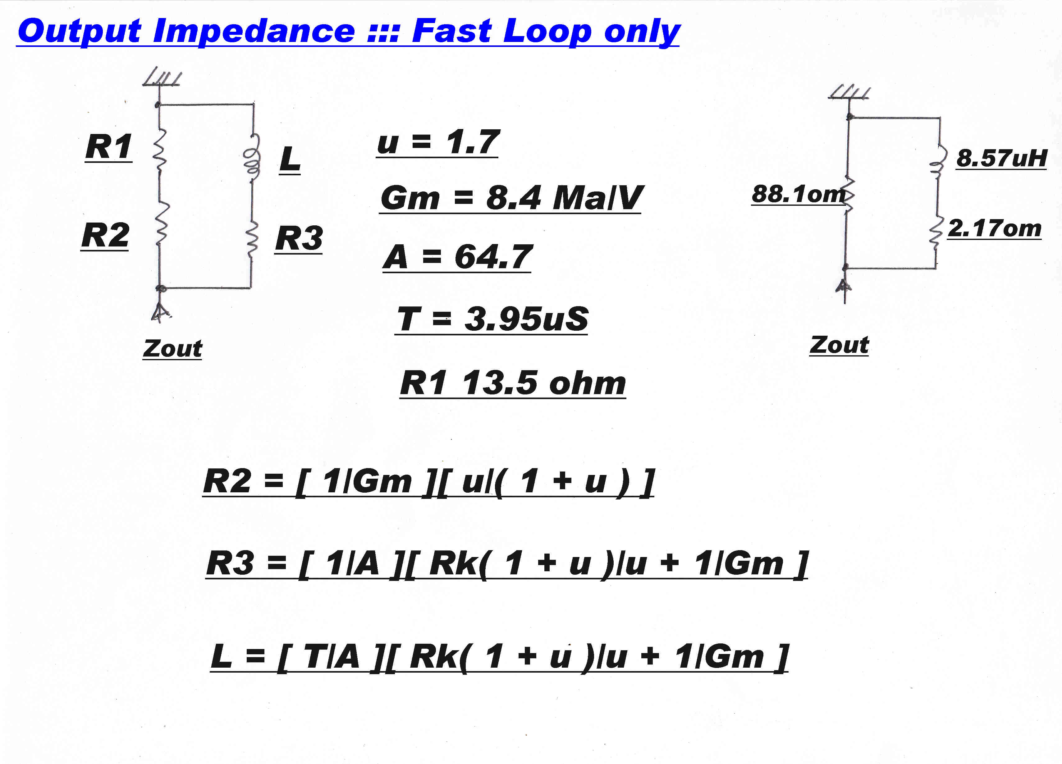
It is instructive to develop the output impedance produced by the HF loop - that is
with the gain of the DC coupled loop put to zero.

|
|
|
Equivalent Circuit for HF Output Stage |
The HF Loop Output Impedance |
The triode is replaced by the equivalent voltage generator -μegk
in series with the plate resistance Rp
Writing the loop equations:-
I = ( Vin - μegk )/( Rk + Rp )
and
egk = eg - ek )
= -VinA/( 1 + τp ) - ( Vin - IRk )
Solving, we get :-
I = V { [ 1/( Rk + Rp/( 1 + μ) ) ]
+ [ μA/( ( 1 + τp )( ( 1 + μ )Rk + Rp ) )] }
Since the input admittance Yin = I/V
Yin = {
[ 1/( Rk + Rp/( 1 + μ) ) ]
+
[ μA/( ( 1 + τp )( ( 1 + μ )Rk
+ Rp ) )] }
This consists of an input conductance
[ 1/( Rk + Rp/( 1 + μ) ) ]
in parallel with an admittance of
[ μA/( ( 1 + τp )( ( 1 + μ )Rk + Rp ) )]
The input conductance gives a resistance of:-
Rk + Rp/( 1 + μ )
in parallel with the impedance:-
[ 1 + τp ][ Rk( 1 + μ)/( μA) +Rp/(μA )]
Or: R3 + R3τp
Where:
R3 = [ 1/A ] [Rk( 1 + μ)/( μ) + Rp/(μ)]
But Rp/(μ) = 1/Gm
So that:
R3 = [ 1/A ] [Rk( 1 + μ)/( μ) + 1/Gm]
And L = R3τ
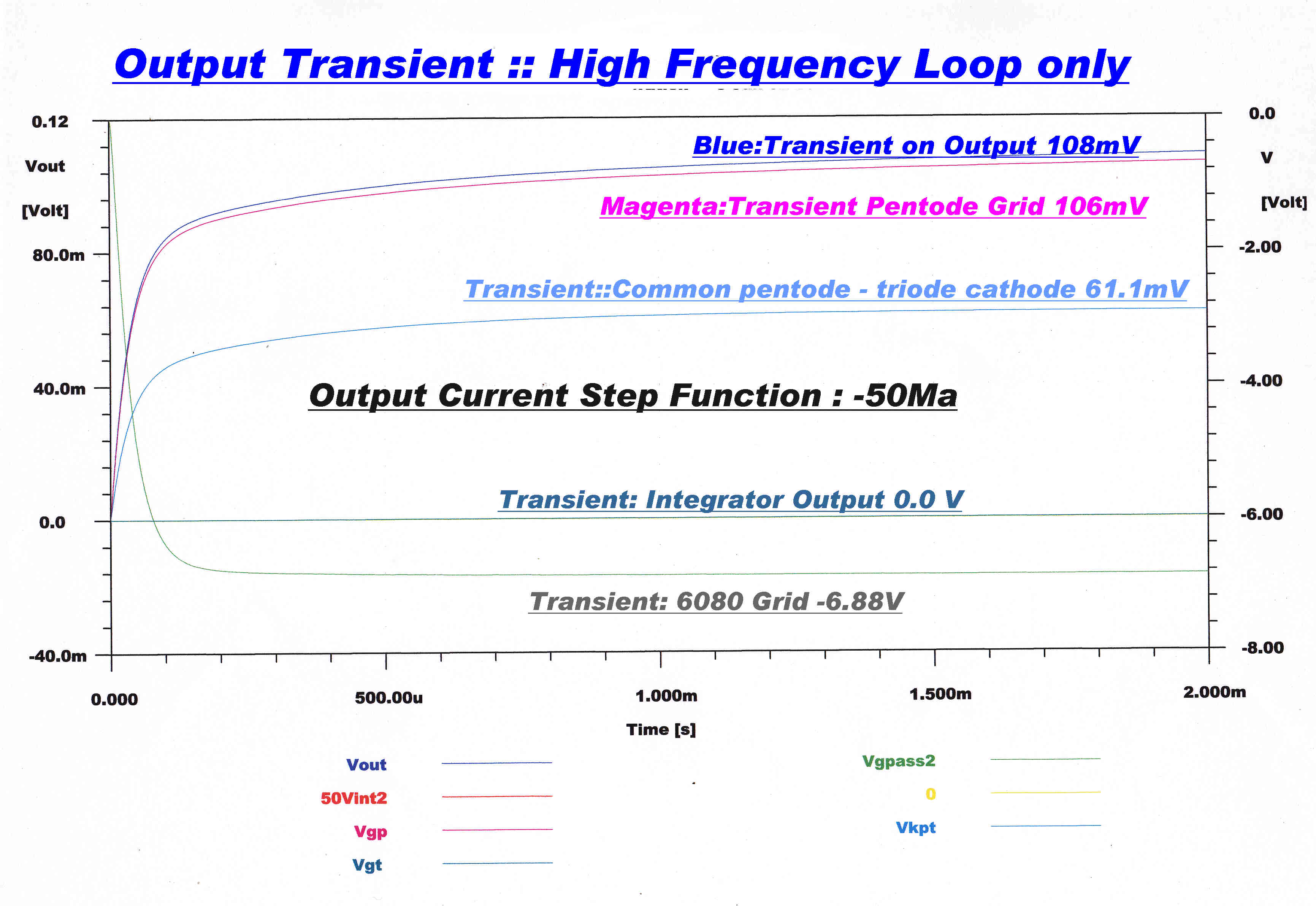
The response of the regulator to a sudden change of -50Ma in load current
is shown below.
The response with only the HF loop active is shown on the left and the total
response on the right.
|
|
|
TRANSIENT RESPONSE : HF Loop Active |
TRANSIENT RESPONSE: HF + LF Loops Active |
 The attenuation of the input ripple is shown in the curves opposite.
Two plots are shown - one with feedforward and one without feed forward.
The feedforward improves the rejection rate by about 20db over the frequency range
from about 1Hz to 2KHz.
Since the feedforward is AC coupled, there is no difference in the rejection rate at 0.1Hz.
 The regulator is driven from a full wave rectifier with capacity input.
The ripple waveform is therefore an asymmetrical saw tooth at 100Hz.
Suppose the main component of this is a 100Hz sinusoid of 50 volts peak.
The waveform at key points of the regulator are shown opposite.
The μ of the 6080 pass tube is 1.7, so that the feedforward produces
a 50/1.7 ( = 29.4) sinusoid on the grid to cancel the hum.
The 100Hz hum on the output is 4.15mV peak.
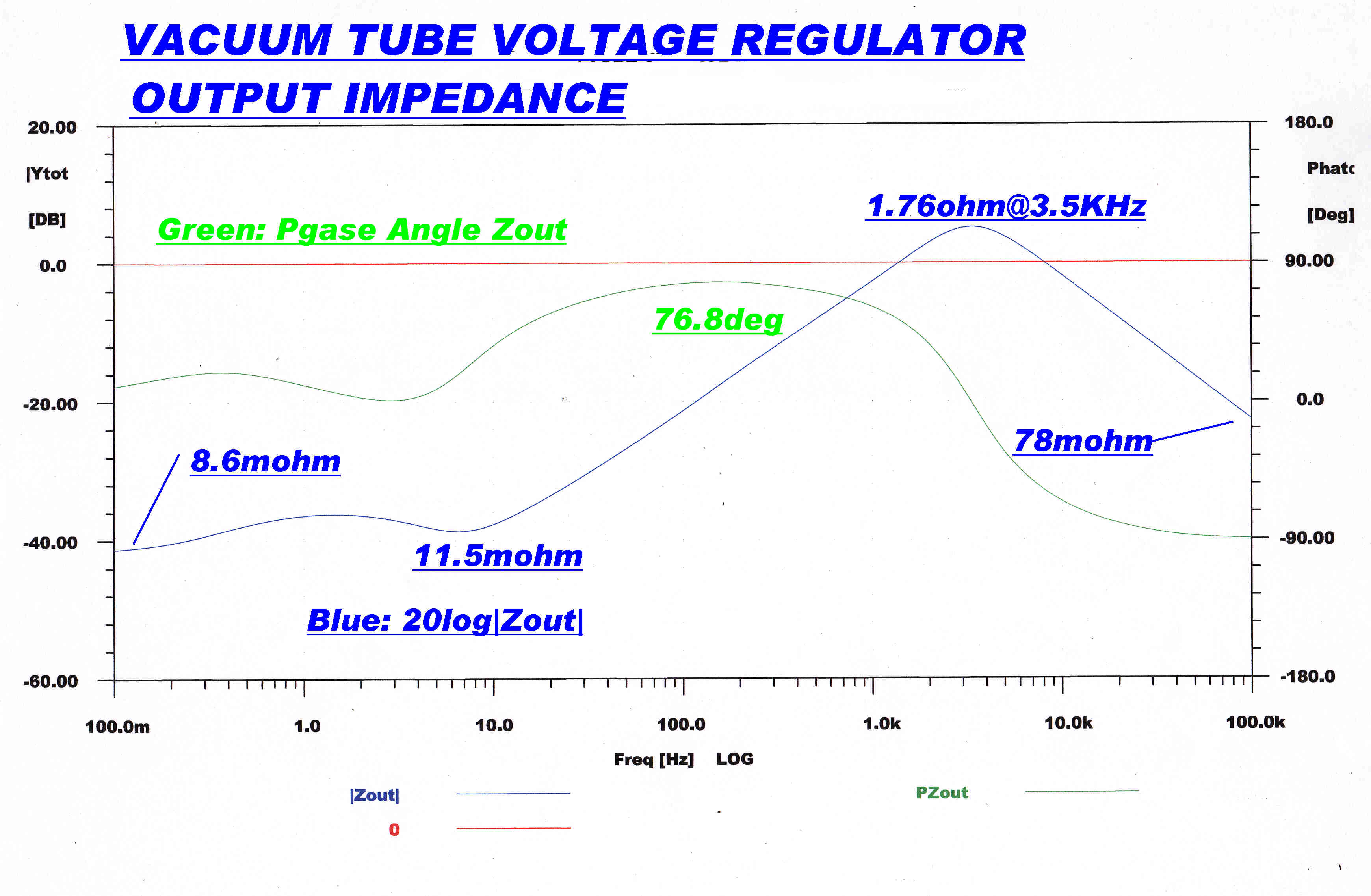 The modulus and phase of the output impedance is shown on a logarithmic scale.
The impedance reaches a minimum of 8.6 milliohms at a frequency of 0.1Hz and stays at
this value down to DC.
Above 10Hz the impedance begins to rise.
This corresponds to a 6db/octave fall in gain in the LF amplifier.
The -90 degree phase change in the LF amplifier produces a highly inductive output impedance.
At 3.5KHz the reactance of the 22uF capacitor across the output has a reactance of 2.06 ohms.
This cancels out the inductive component produced by the feedback and results in a peak in the
impedance of 1.76 ohms. This is purely resistive.
The output impedance at 100KHz is 78 milliohms and purely capacitive.
The reactance of the 22uF capacitor at 100KHz is 72.34 milliohms.
The output impedance at 100KHz is therefore determined mainly by the 22uF output ccapacitor.
![]() The transient on the regulator output is plotted for a step function
in load current of - 50Ma.
The transient on the regulator output is plotted for a step function
in load current of - 50Ma.
The shape of the transient is determined mainly by the HF loop for the first 50uSec.
By 130uSec the LF amplifier has nearly reached its final value.
The "DC" output resistance is 8.6x10⁻³ ohms.
So the output will ultimately change by 50x10-3 x 8.6x10-3
= 0.43mV