HIGH FIDELITY AM TRANSMITTER
CONTACT : COMMENTS AND QUESTIONS
back/home
It is not difficult to achieve the full audio bandwidth in transmitters : reducing the
overall harmonic distortion to 0.1% or below does present some difficulties.
Almost all of these occur in the modulator.
 At first glance, envelope feedback around the modulator seems attractive.
The distortion of an envelope feedback modulator cannot be lower than the distortion of the
detector providing the feedback.
Most of these detectors are product demodulators which can also be used directly as a modulator,
so there is nothing to be gained from feedback. Direct modulation will give the same result
with less complication.
Modulators which give carrier cutoff at 100% negative modulation also present problems
in feedback loops.
During cutoff when the loop gain goes to zero, large errors can build up in the loop resulting
in paralysis for considerable periods.
Product modulators and demodulators which respond to overmodulation in the negative direction
prevent this.
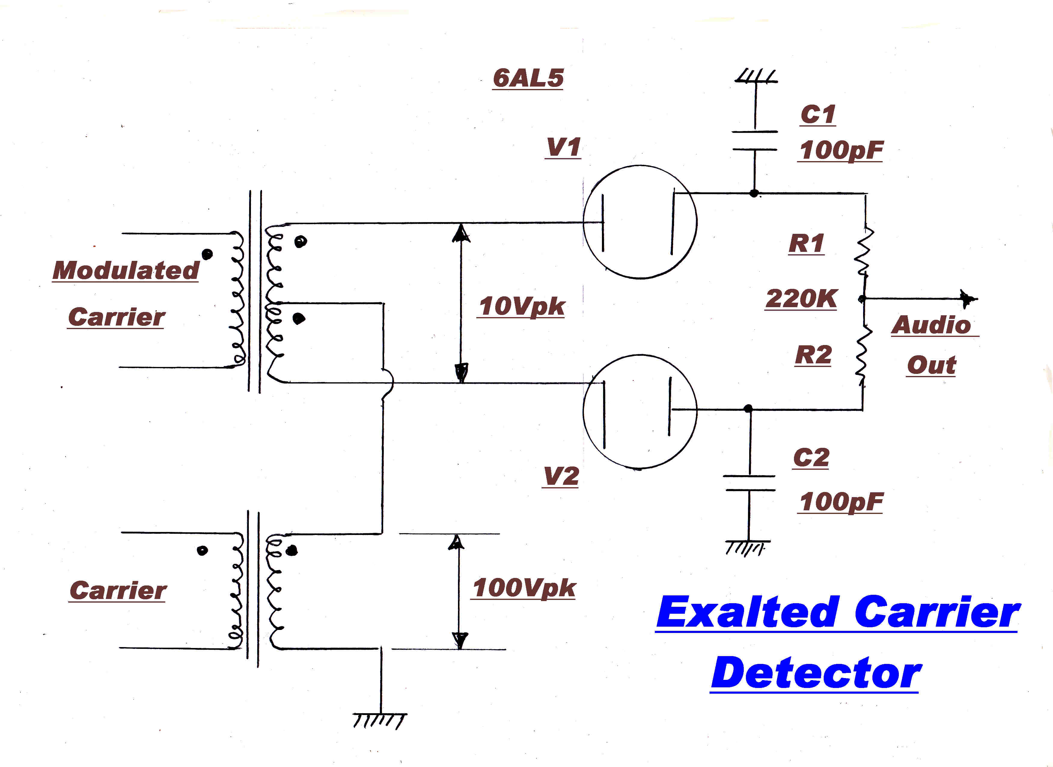
The exalted carrier demodulator shown on the right is capable of low distortion product
demodulation and is frequently used for envelope feedback.
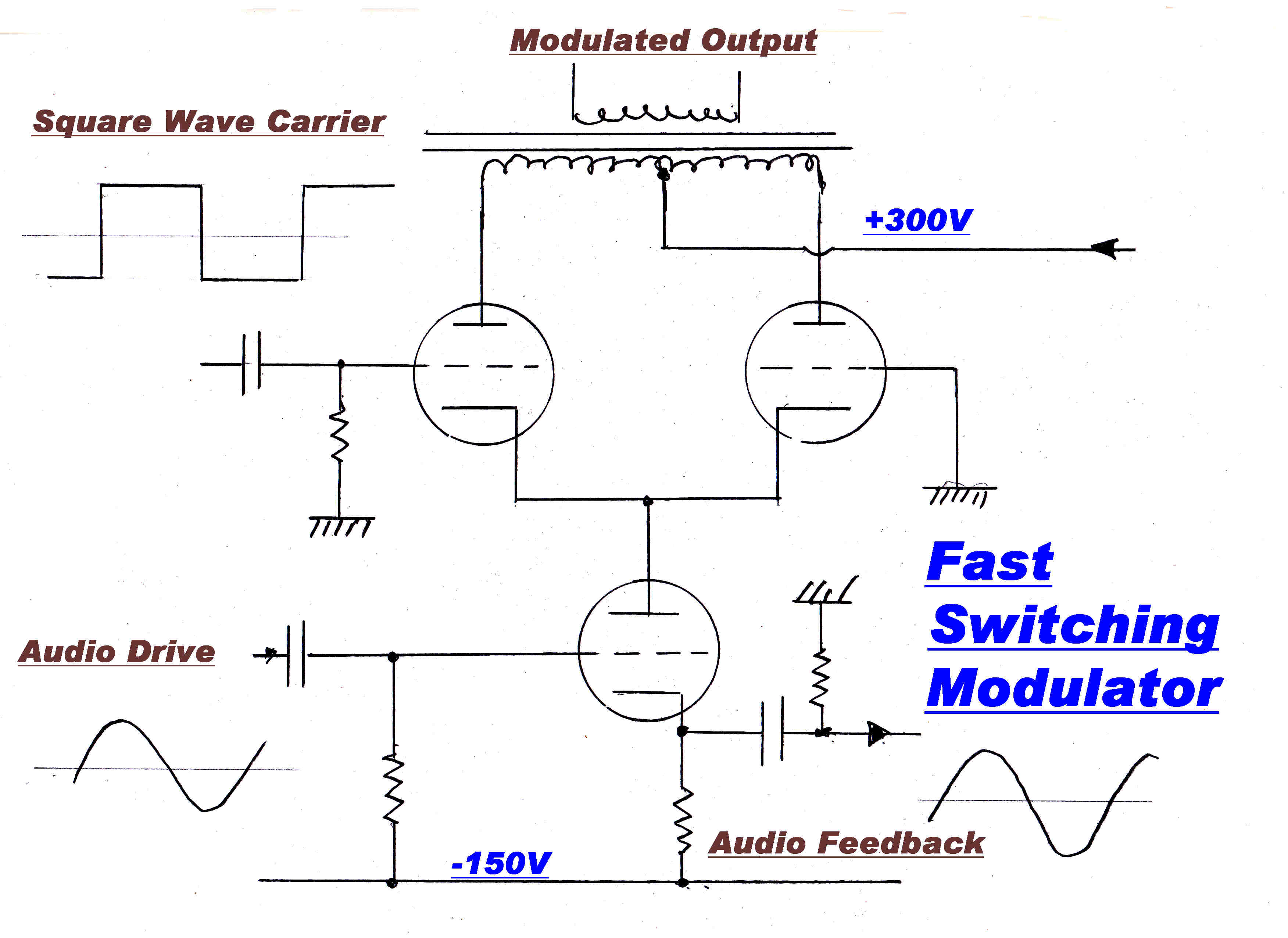
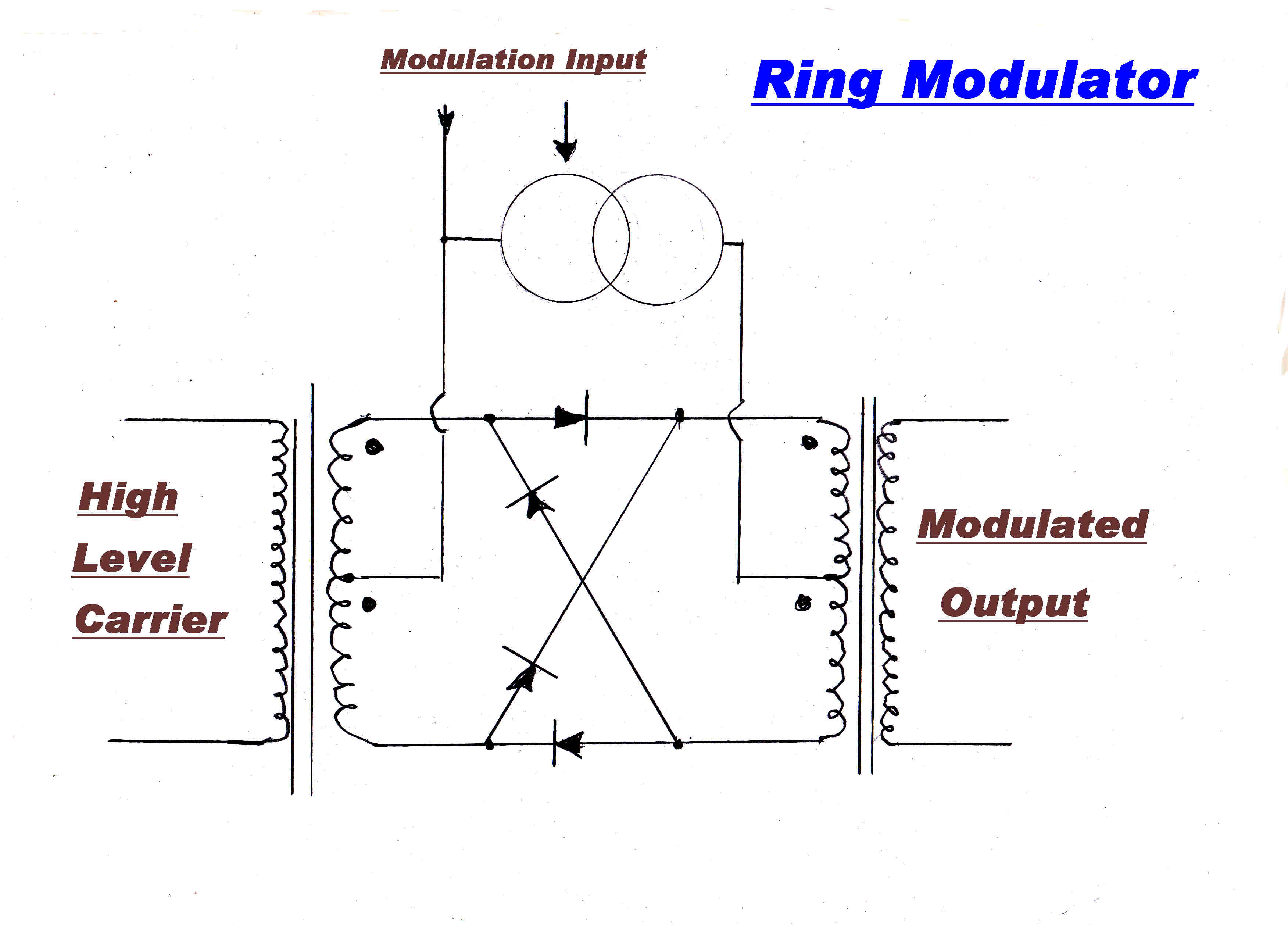 A ring modulator is shown on the right followed by a vaccum tube equivalent.
Here the modulating signal is switched by a square wave at carrier frequency into a
resonant circuit.
The switch is either fully on carrying the total modulating signal or fully off,
so that the transfer characteristic of the switch (non-linear behaviour) does not matter.
In the ring modulator the carrier drive is usually sinusoidal, but of high amplitude
to approximate square wave switching.
 Since AM is a simple process where the carrier is multiplied by the modulating signal,
any fast accurate solid state multiplier will generate low distortion AM.
Since AM is a simple process where the carrier is multiplied by the modulating signal,
any fast accurate solid state multiplier will generate low distortion AM.
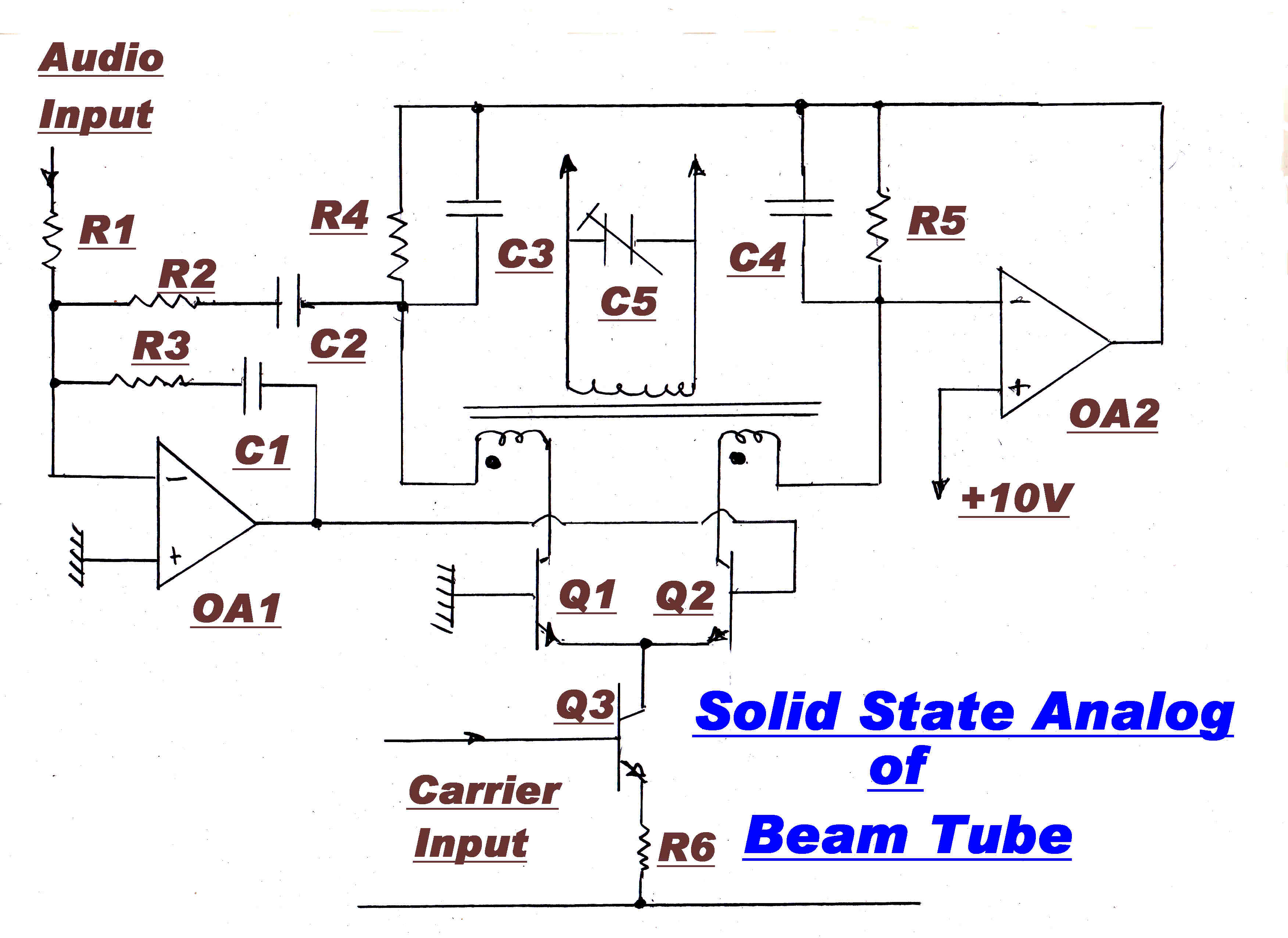
A simple and accurate multiplier can be made from an emitter driven long tail pair as
shown opposite.
A DC current with a small carrier component imposed on it is injected into the common
emitters of Q1 and Q2 by Q3.
The small RF current changes with the collector current balance of Q1 and Q2 giving AM.
If the transfer characteristic of Q1 and Q2 is exponential* then the RF
current split is the same as the collector current split.
If the difference between the collector currents of Q1 and Q2 is a linear function
of the modulating signal there will be no distortion.
The difference current is sensed by R4 R5 and is used for heavy feedback to ensure linearity.
* This is proved in the AGC section of the AM Tuner.
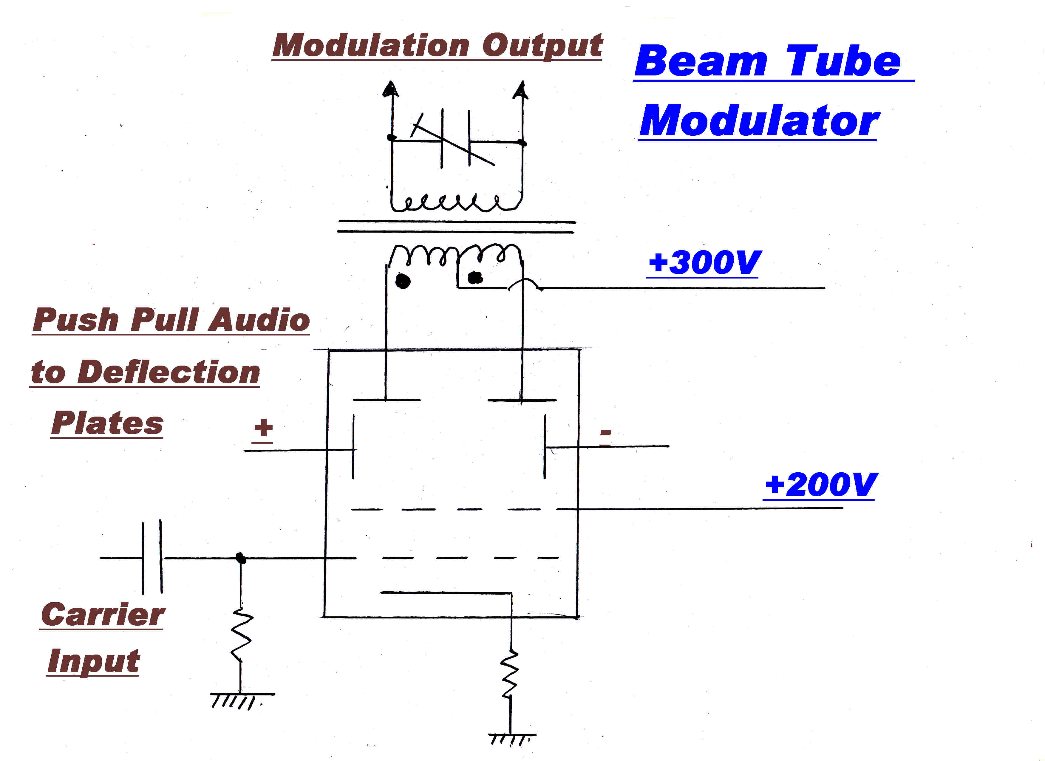
The long tail solid state pair may be replaced by a beam deflection tube in a valve transmitter.
Here the current split is a linear function of the voltage drive, so that the distortion is reduced.
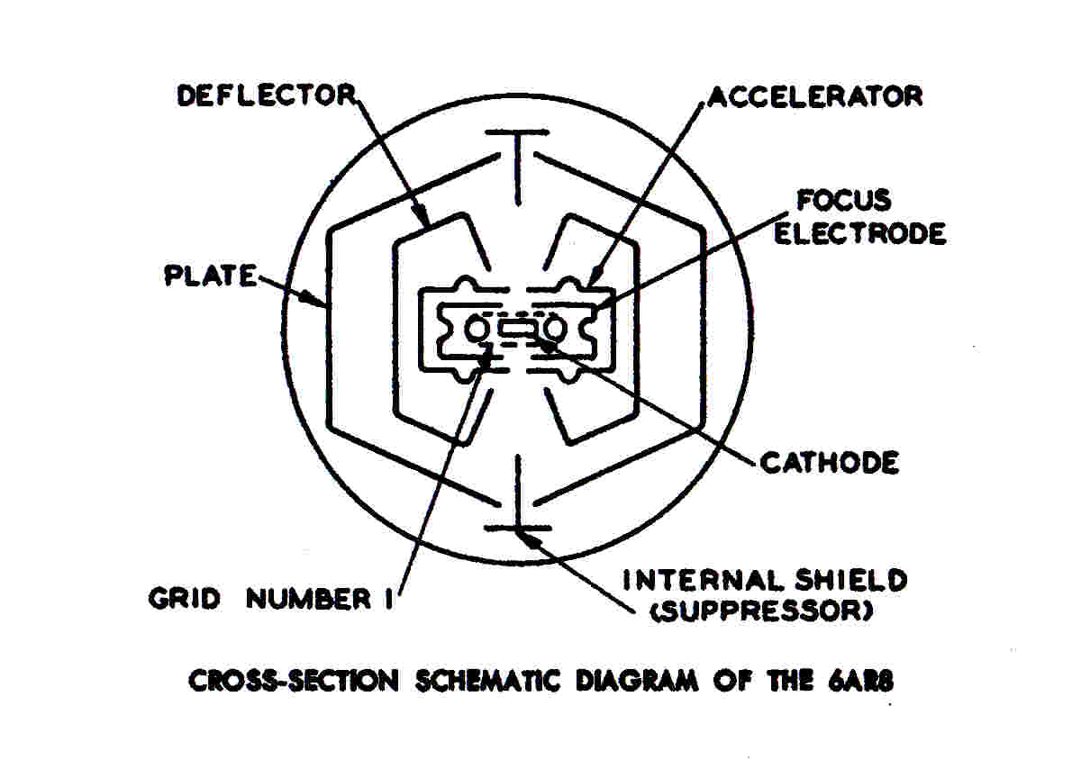
 The construction of the tube and its characteristics are shown on the right.
An electron beam of rectangular cross section is deflected by two deflection plates and
intercepted by a split anode.
The strength of the beam can be modulated by a grid near the cathode.
If the beam is modulated at RF and push-pull audio applied to the plates, an amplitude modulated
signal will appear in both plates.
If only the middle portion of the deflection characteristic is used, the modulation distortion
is very low.
As the beam current increases, mutual repulsion between the electrons causes the beam to spread,
so a greater deflection voltage is required to totally deflect the beam at high beam currents.
If a small radio frequency sinusoidal signal modulates the beam current, it is assumed that it
splits in the same ratio as the total beam current. Beam spreading may introduce a small
second order error. This can be made insignificant by reducing the fractional beam modulation
by the RF carrier applied to the control grid.
In all further work it will be assumed that the fractional split of the small signal RF component
is proportional to the fractional split of the beam current.
This assumption can be illustrated by a simple algebraic analysis.
This non- rigorous analysis is an attempt to give an intuitive understanding of
of the beam tube defection.
Imagine the plates of the deflection tube coated with flourescent material.
The electrom beam would produce a bright rectangle moved linearly along the x axis by the deflecting
plate voltage. If a small RF voltage is applied to the control grid to modulate the strength of
the electron beam, the vertical edges of the rectangle would become blurred, since the beam width
increases with current density.
The middle portion would dim slightly, since a small fraction of the current is diverted to the
extended edges.
If this whole system is shifted linearly in the x direction by a change in deflection voltage,
it seems reasonable to assume that the amplitude of the RF component also changes in a linear
fashion.
If the deflection from the central position is to the right, then the fractional increase
in width is less than the fractional increase to the left, so a small decrease in the deflection
sensitivity would be expected.
A short algebraic analysis also bears this out.
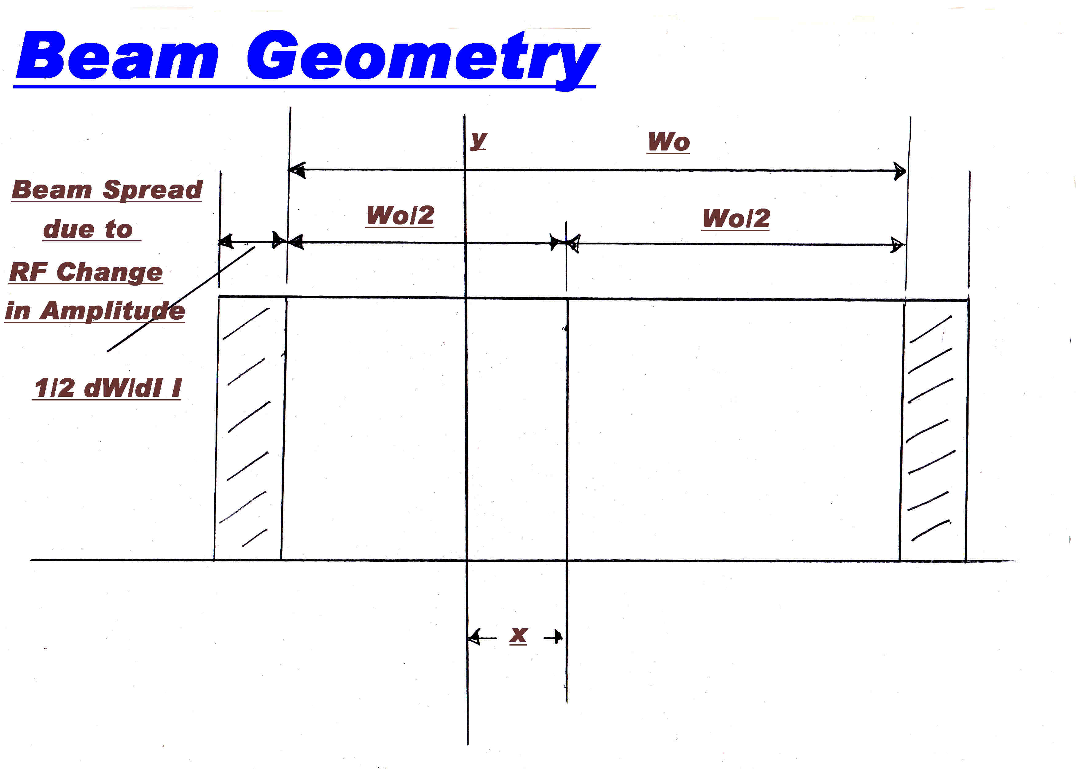 A diagram of the beam area on the plates is shown on the right.
Assume that the increase in beam width W with total current I is represented by the
equation:-
W = Wo + (dW/dI) I
where (1/Wo)(dW/dI) << 1
If the centre of the beam is deflected by a distance x then the total length of the beam Wr
on the right anode is:-
Wr = x + Wo/2 + 1/2 dW/dI I
and for Wl on the left:-
Wl = -x + Wo/2 + 1/2 dW/dI I
Then the total current to the right is given by:-
Ir = I x [ Area on Right / Total Area ]
Note:This implies that the electron density across the beam is uniform.
So Ir = I [ x + Wo/2 + 1/2 dW/dI I ] / [ Wo + dW/dI I ]
= I [ Wo/2 + 1/2 dW/dI ] / [ Wo + dW/dI I ] + I x / [ Wo + dW/dI I ]
= I/2 + I x / [ Wo + dW/dI I ]
≈ I/2 + I x/Wo [ 1 - 1/Wo dW/dI I ]
Since 1/Wo dW/dI <<1
Then Ir ≈ I [ 1/2 + x/Wo ( 1 - 1/Wo dW/dI I ) ]
The system has remained linear in x but the deflection sensitivity has been reduced by the factor:-
( 1 - 1/Wo dW/dI I )
Suppose we perturb the current I with a small increase in cathode current Δ I
A bit of algebra then shows that:-
Ir ≈ Io [ 1/2 + x/Wo ]
- Io[ x/(Wo)2 dW/dI Io ]
+ Δ I [ 1/2 + x/Wo ]
- Δ I [ 2x/(Wo)2 dW/dI Io ]
The first term Io [ 1/2 + x/Wo ] gives the expected change in the bulk plate
currents with no error.
The second term - Io[ x/(Wo)2 dW/dI Io ] gives the
error in the bulk current. Note that this would be corrected by the overall feedback loop.
The third term + Δ I [ 1/2 + x/Wo ] gives the change for the current increment Δ I
with no distortion.
The fourth term - Δ I [ 2x/(Wo)2 dW/dI Io ] gives the error
in this change. It is twice the error for the bulk plate current.
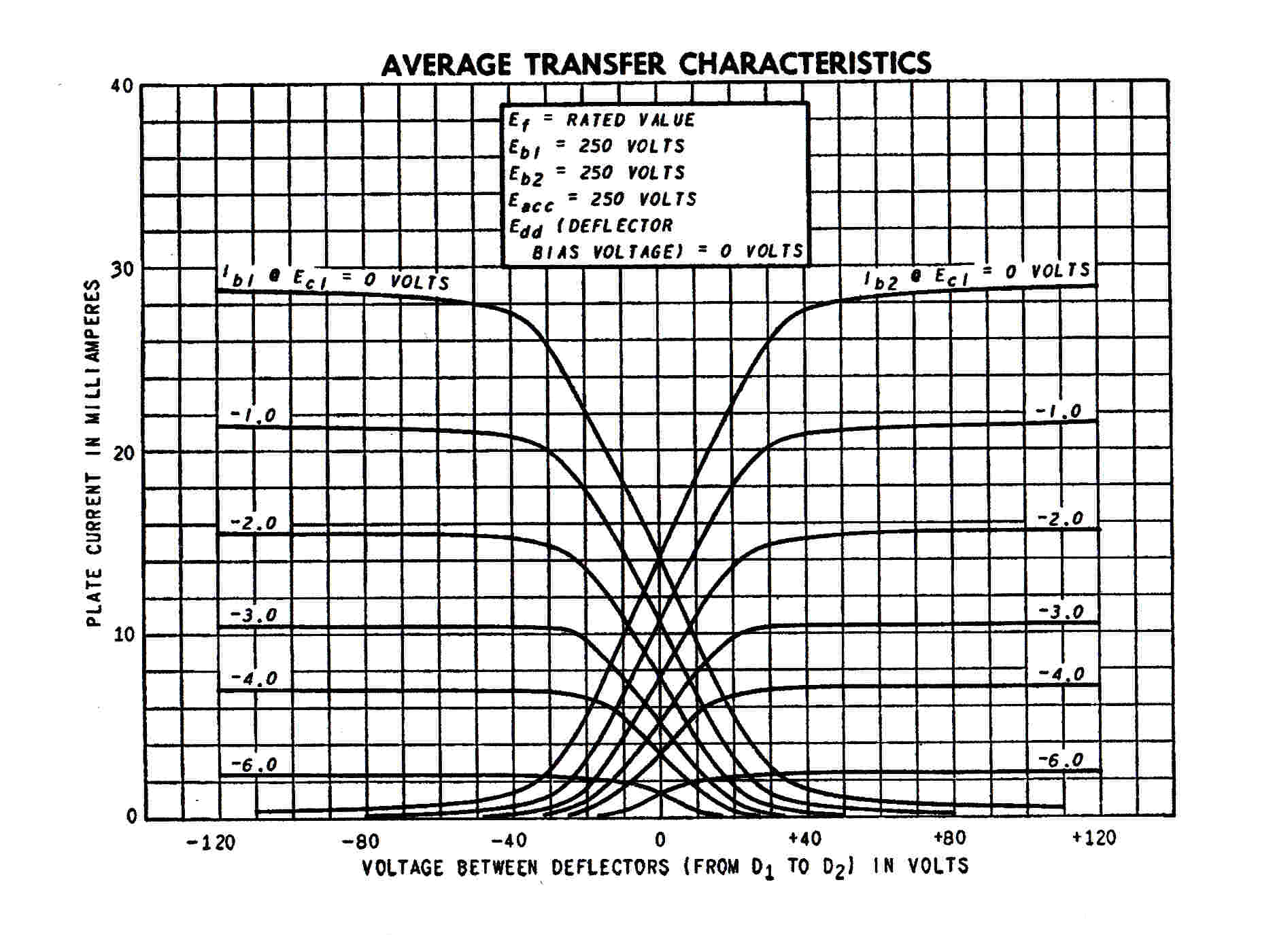
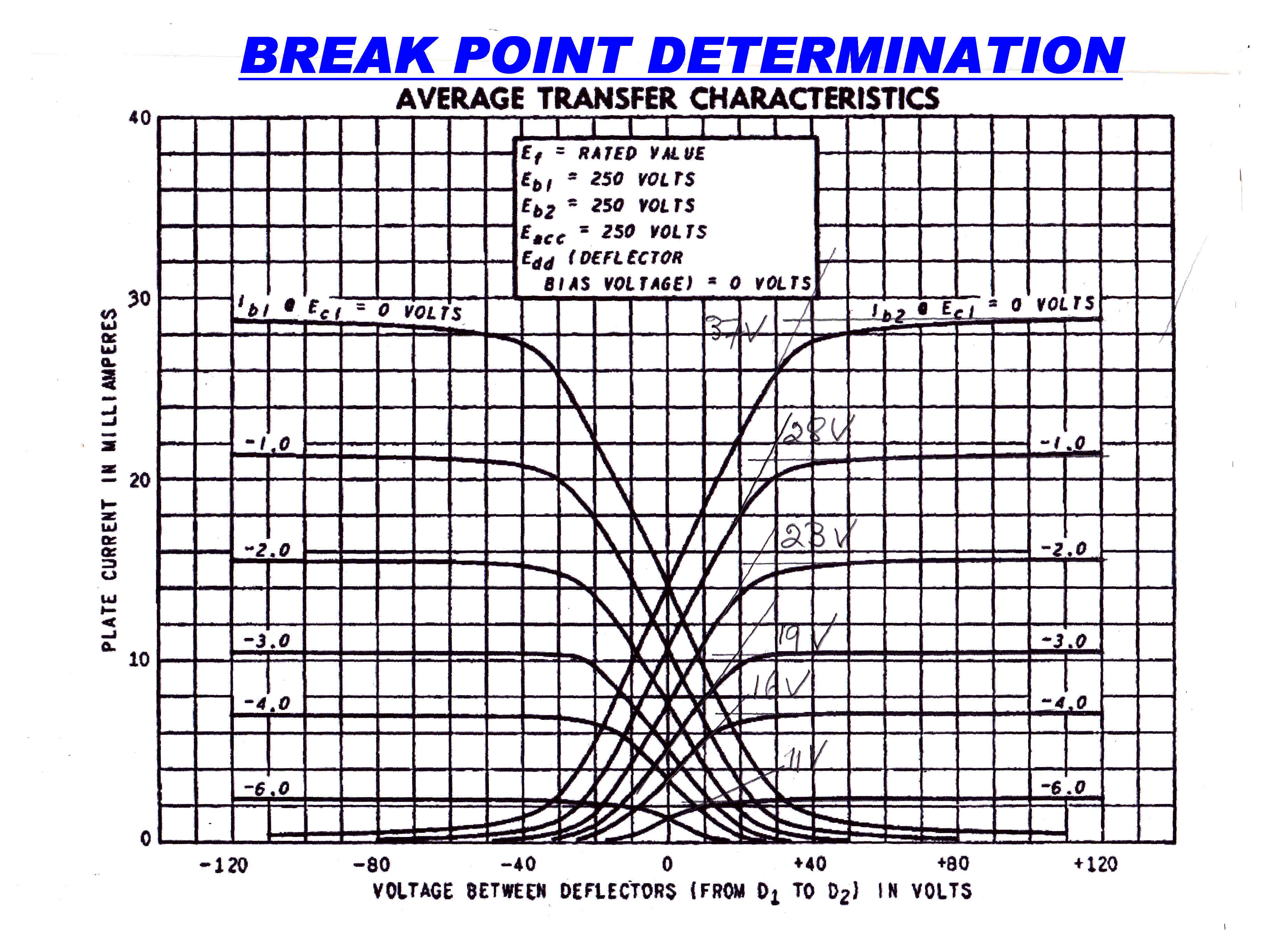
This analysis relies on the published deflection curves for the 6AR8 beam tube.
It is independent of any model adopted for the deflection system, and so is purely algebraic
and non intuitive.
The first task is to represent the graphical deflection curves in algebraic equations.
The break points are determined for curves with no rounded shoulder.
The break points are then plotted against the undeflected beam current for one plate for varying
biases on grid 1.
|
|
|
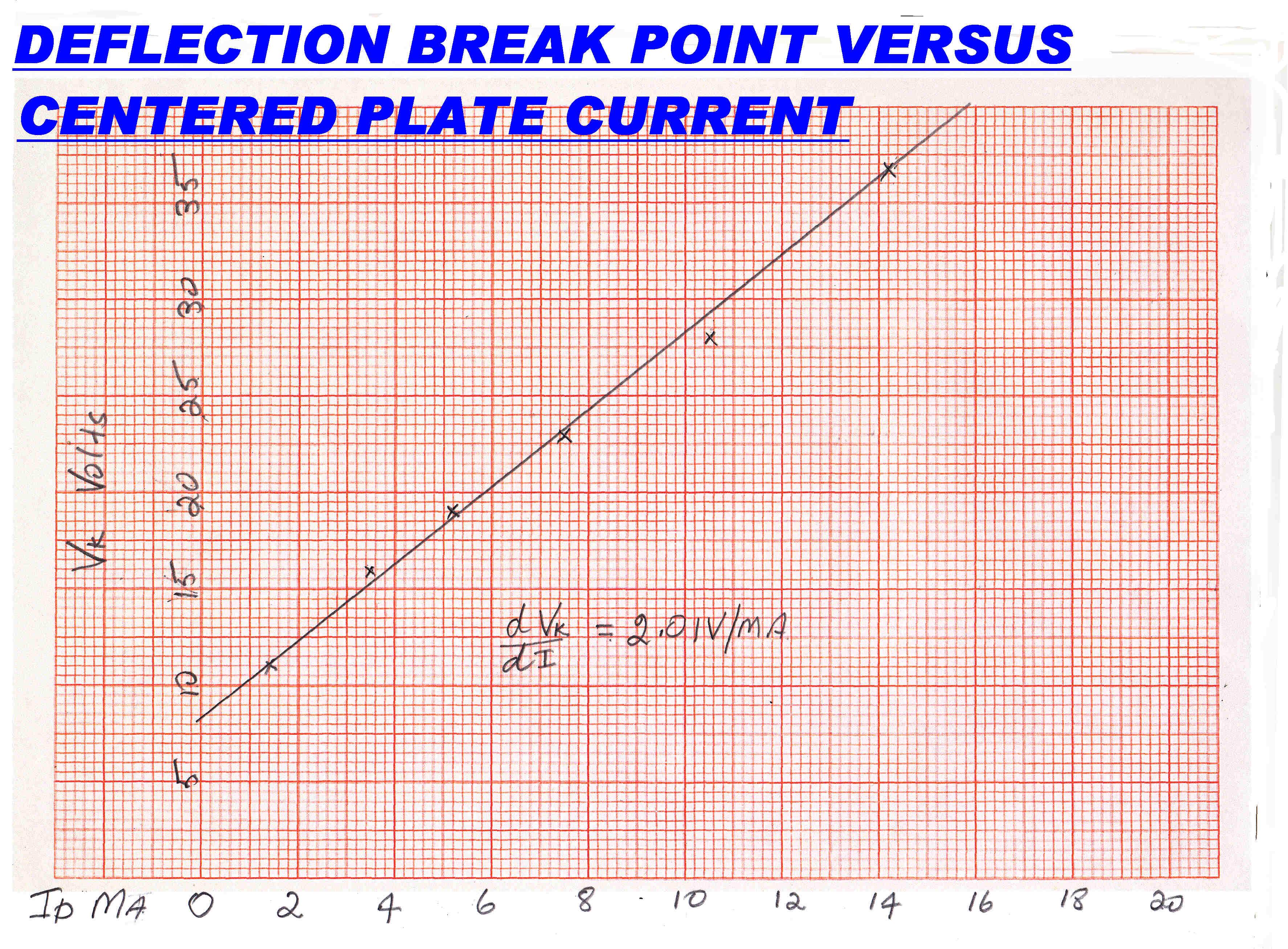
The curves are extended as if completely linear to find the break point. |
The break point is now plotted against the undeflected plate current of one plate. |
The transmitter operates in the middle of the deflection curves, so we can write
with some accuracy:-
i = I [ 1 + V/VK ]
where:-
i is the current in one plate for the deflection voltage V with a break voltage of VK
I is the undeflected current in the plate.
From above:-
VK = α + β I
So we have:-
i = I [ 1 + V/( α + β I ) ]
Suppose we now make a small perturbation ΔI to I by applying a small amount of RF to grid 1
Then:-
i + Δi = [ Io + ΔI ]
[ 1 + V/( α + β ( Io + ΔI ) ) ]
Note: Δi is the change in the plate current when it is deflected by the deflecting voltage V
ΔI is the change in the plate current in the centered or undeflected position.
After some tedious small signal algebra using the binomial theorem, the above equation gives:-
Δi = ΔI [ 1 + ( V/VK )( 1 - Io/VK dVK/dI ) ]
+ ( ΔI )2 V/VK2 dVK/dI
[ (Io/VK) dVK/dI - 1 ]
Examination of the equation shows that:-
[1] If dVK/dI = 0 the equation reduces to:-
Δi = ΔI [ 1 + ( V/VK ) as expected
[2] The deflection is still a linear function of V - the deflecting voltage - although the sensitivity has been reduced
by:-
( 1 - Io/VK dVK/dI )
More physical insight is given by rewriting this expression as:-
( 1 - dVK/dI / ( VK/ Io ) )
[3] When the perturbation is sinusoidal the ( ΔI )2 term gives rise to a small DC offset and
second harmonic of the carrier.
Both are rejected by the tuned circuit in the plate.
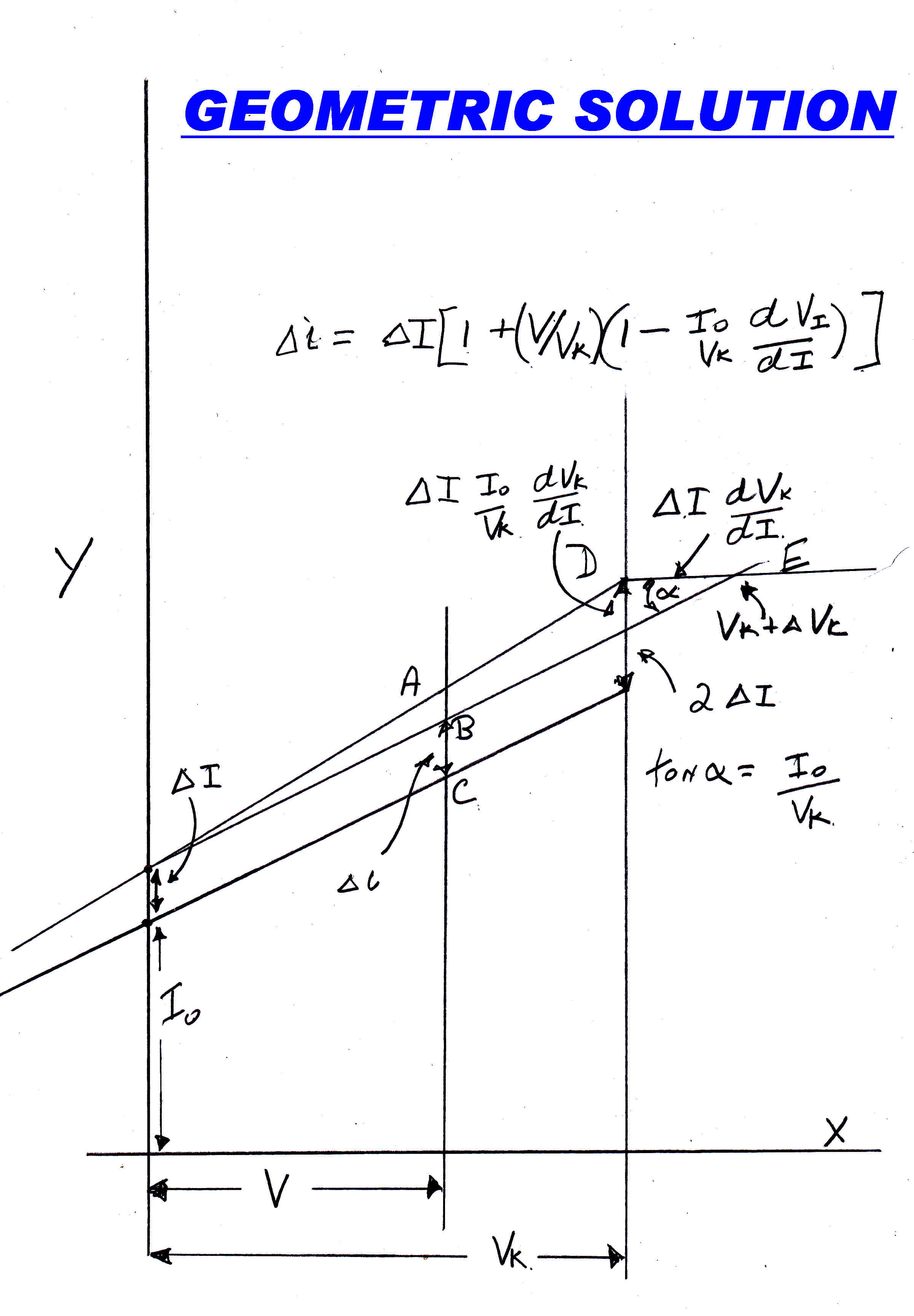 A geometric analysis consistent with the above small signal algebra is shown on the right.
A small RF voltage on the first grid produces a change ΔI in the undeflected current on one plate.
If the deflection sensitivity did not decrease with current, then the deflection current would follow the line AD.
But the deflection sensitivity has been decreasaed by the increase in break voltage DE
The deflection is still linear, but has been decreased by the ratio BC/AC
From the geometry:-
Δi = ΔI + ΔI V/VK - ΔI Io/VK dVK/dI V/VK
That is:-
Δi = ΔI [ 1 + ( V/VK )( 1 - Io/VK dVK/dI ) ]
The result of the algebraic analysis.
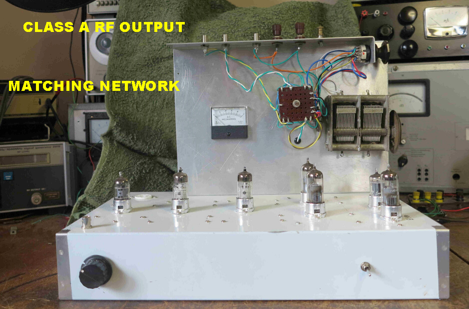
The low power transmitter consists of two sections:-
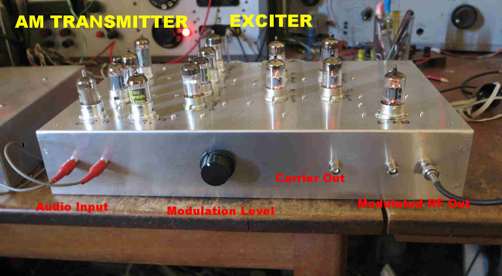 [A] An exciter which contains:-
[B] A power amplifier which contains:-
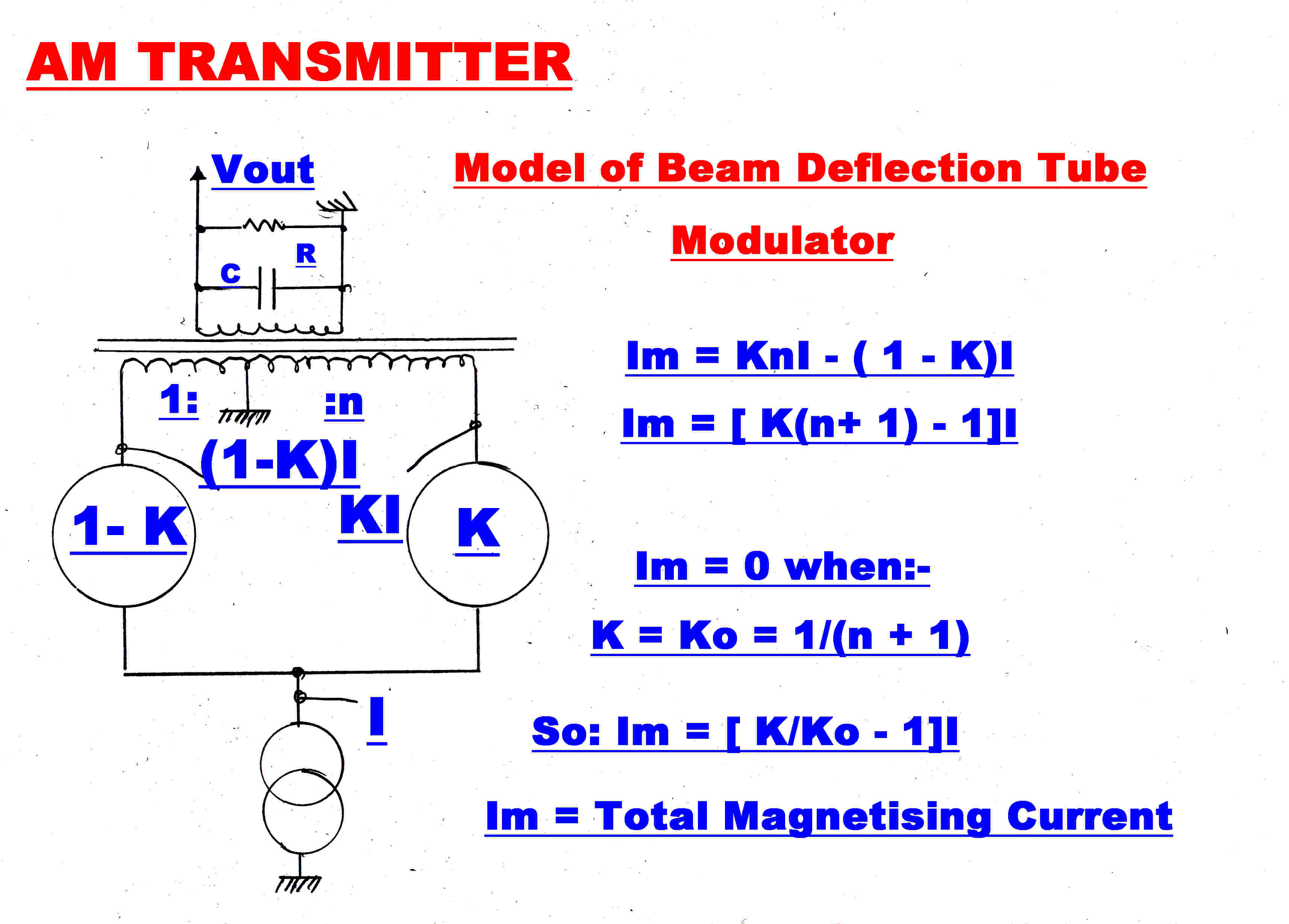 A simplified model of the beam deflection tube is showm on the right.
I is the total beam current.
A fraction K is directed to the RH side giving a current = KI.
This leaves ( 1 - K )I on the LH side.
The transformer primary windings have a ratio of 1:n
The total magnetising current Im is then given by:-
Im = KnI - ( 1 - K )I
∴ Im = [ K(n + 1) - 1 ]I
When used as a modulator, zero carrier condition occurs when Im = 0 at Ko
∴ 0 = [ Ko(n+ 1) - 1 ]I
∴ Ko = 1/( 1 + n )
So that :- Im = [ K/Ko - 1 ]I
Unmodulated carrier occurs when K = 1/2
So that : Imc = [ 1/2Ko - 1 ]I
100% modulation gives a peak carrier of 2Imc = Imp
So:- Imp = 2[ 1/2Ko - 1 ]I
The ratio Kp for peak carrier is then given by:-
[ Kp/Ko - 1 ]I = 2[ 1/2Ko - 1 ]I
∴ Kp = 1 - Ko
In the transmitter n = 2 so that:-
Ko= 1/3
Kc = 1/2
Kp = 2/3
For full modulation the current division swings between 1/3 and 2/3 : that is only
over the linear portion of the deflection characteristic.
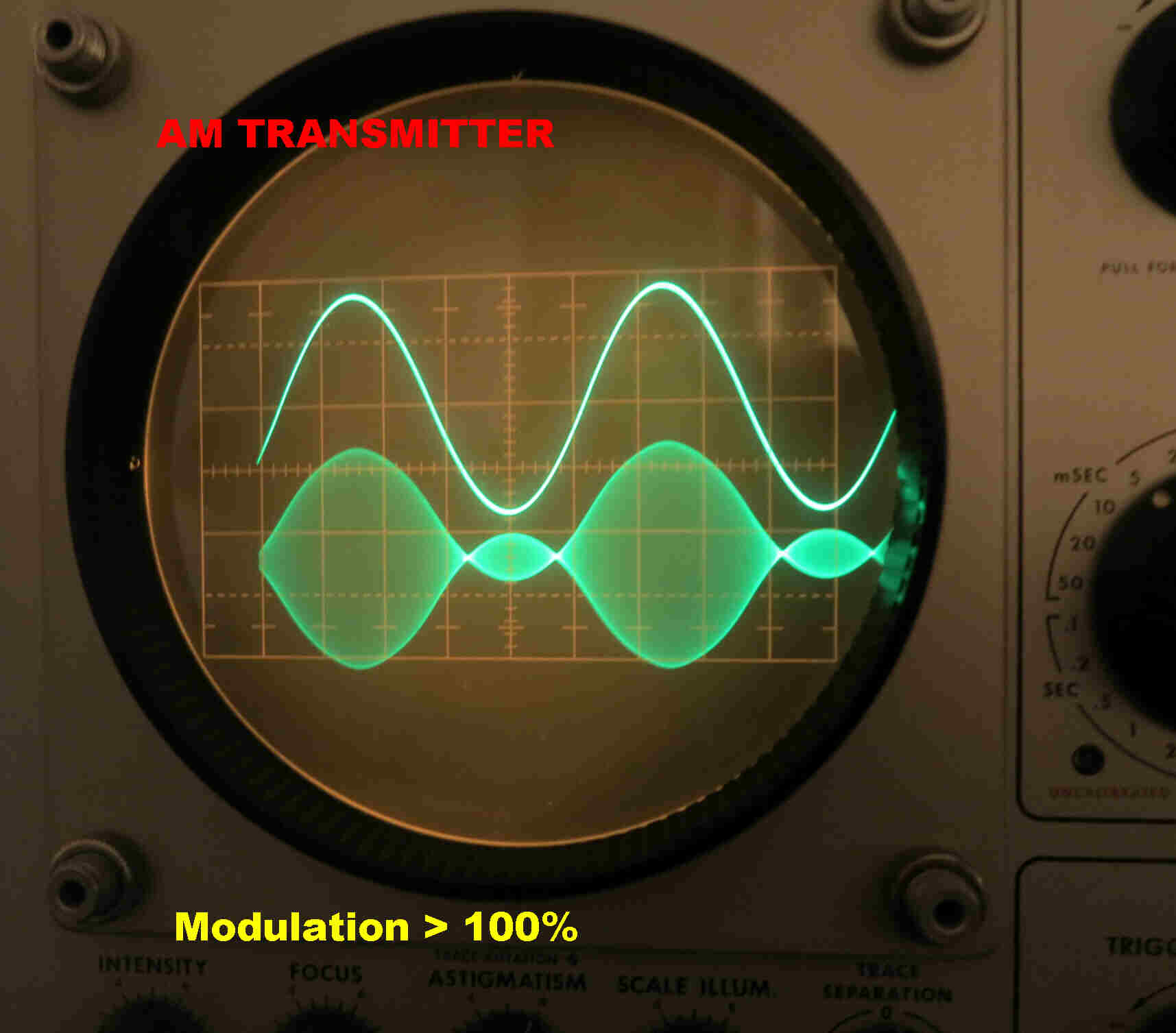
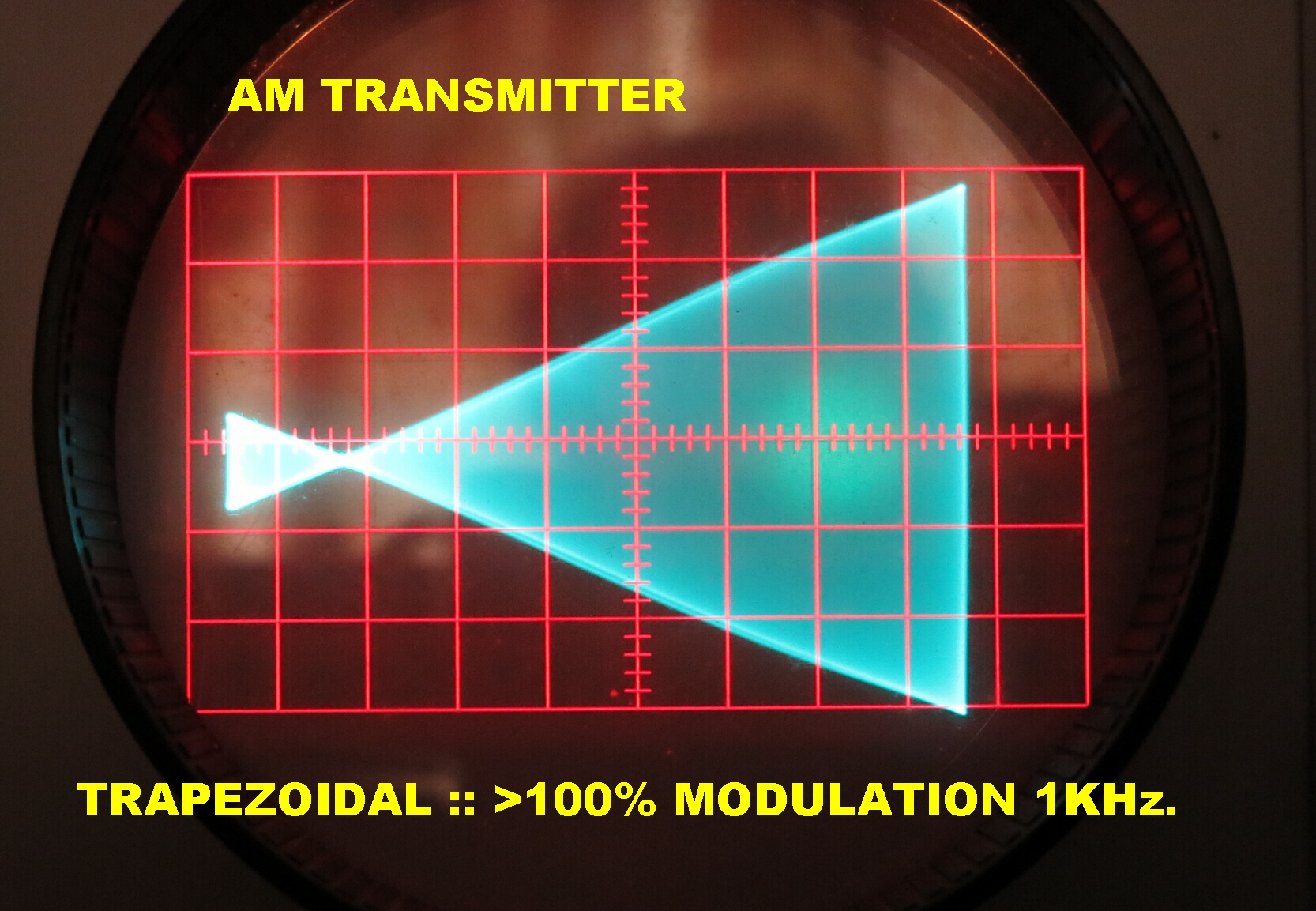 This modulator is capable of producing greater than 100% modulation
in the negative direction.
This modulator is capable of producing greater than 100% modulation
in the negative direction.
An envelope detector produces horrendous distortion under these conditions,
but the product demodulators in the Tuner demodulate the signal correctly.
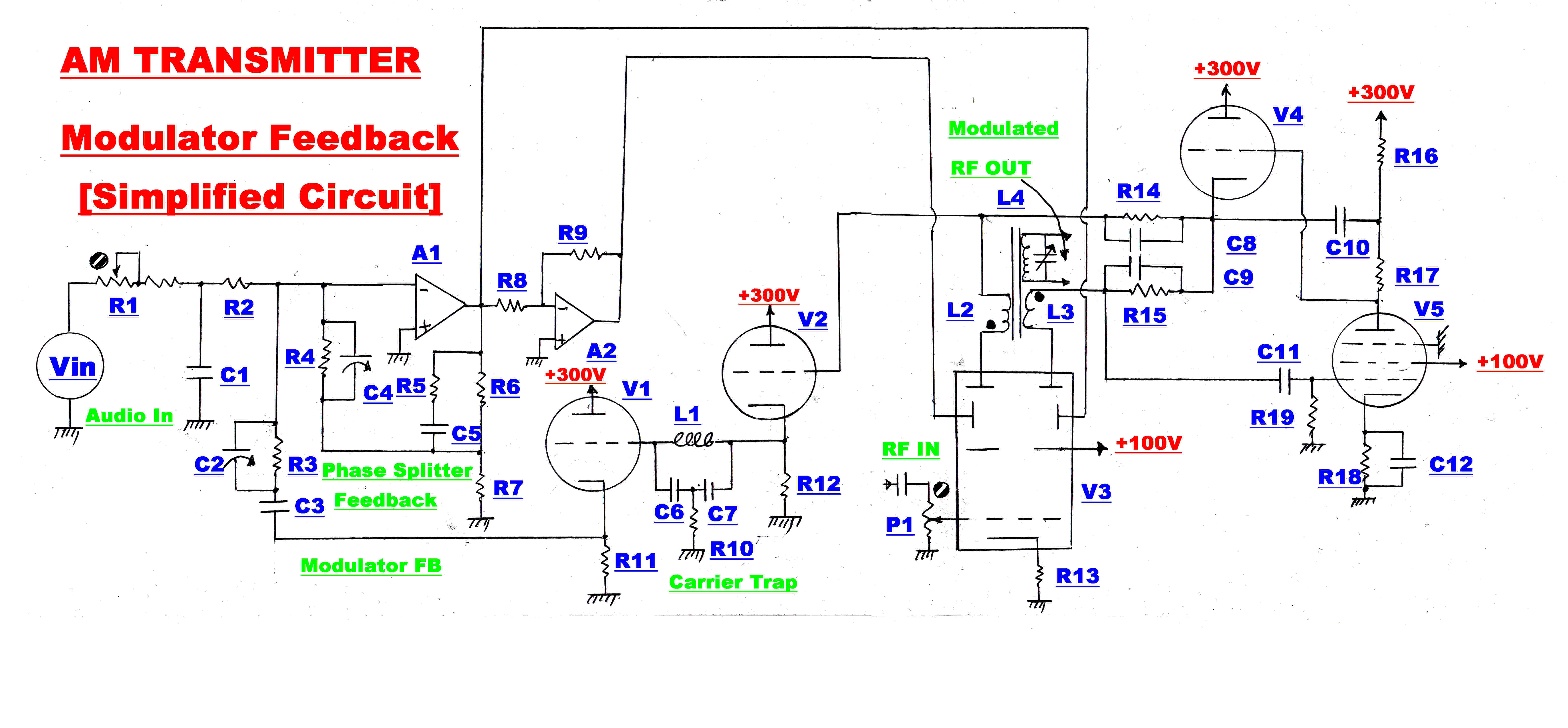 A simplified circuit diagram of the modulator feedback is shown above.
The modulator distortion is inherently low since the deflection curves for the
beam deflection tube are linear and only the central portion is used for full modulation.
As a further guard against distortion, 26db ( x20) overall feedback is applied to
improve the deflection linearity of the beam tube.
The RF modulation is a linear function of the difference between the left hand
plate current, Ilhp, and right hand plate current, Irhp, of the beam tube V3.
The variable ( Ilhp - Irhp ) must be used for feedback.
V4 and V5 form an operational amplifier with the gain increased by boot strapping through C10.
R15 is the feed back resistor, so the voltage on the cathode of V4 is given by:-
V4c = -IrhpR15
The voltage on the left hand plate of V3 is then:-
Vlhp = IlhpR14 - IrhpR15
But R14 = R15
So: Vlhp = ( Ilhp - Irhp )R14
Here R14 = R15 = 1.8K
The currents Ilhp and Irhp contain an RF component at
carrier frequency and this must be kept out of the modulator feedback loop.
R14 and R15 must therefore be bypassed.
This produces a pole in the feedback loop which can be used as the main stabilising pole.
Unforunately, the pole is in the feedback path not the forward path.
For a simple feedback system:-
Y(p) = A(p)/( 1 + A(p)β(p) )
where Y(p) is the closed loop response:: A(p) is the forward open loop response::
β(p) is the feedback transfer function.
Here A(p) = A the forward gain.
β(p) = 1/( 1 + RCp )
where R = R14 = R15 = 2.7k
and C = C8 = C9 = 1.8nF
The turnover frequency fp is given by:- fp = 1/( 2ΠRC ) = 32.75KHz.
This is chosen as low as possible while still keeping it above the audio band.
Subsituting β(p) in the above equation we get:-
Y(p) = [ A/( 1 + A ) ][ (1 + τp )/( 1 + τp/( 1 + A ) ) ] where τ = RC
A zero has been introduced into the closed loop response.
This must be cancelled by a corresponding pole introduced into the signal path before
the feedback modulator.
If we introduce the correction transfer function Yc(p) we get :
Yc(p) = 1/( 1 + τcp )
The total transfer function Ytot(p) is given by:-
Ytot(p) =
[ A/( 1 + A ) ][ 1/( 1 + τcp ) ][ (1 + τp )/( 1 + τp/( 1 + A ) ) ]
For compensation: τ = τc so that :-
Ytot(p) = [ A/( 1 + A ) ][ 1/( 1 + τp/( 1 + A ) ) ] ::
a single pole shifted out by ( 1 + A ).
Here A = 20, so the compensated modulator has a turnover frequency of 21x32.75KHz. = 687.75KHz.
 Compensation Network
The compensation pole at -1/τc is produced by the input network R1,R2,C1.
The input terminal of A1 is a virtual earth, so the driving point impedance to C1
is R1 and R2 in parallel to give:-
τc = C1R1R2/( R1 + R2)
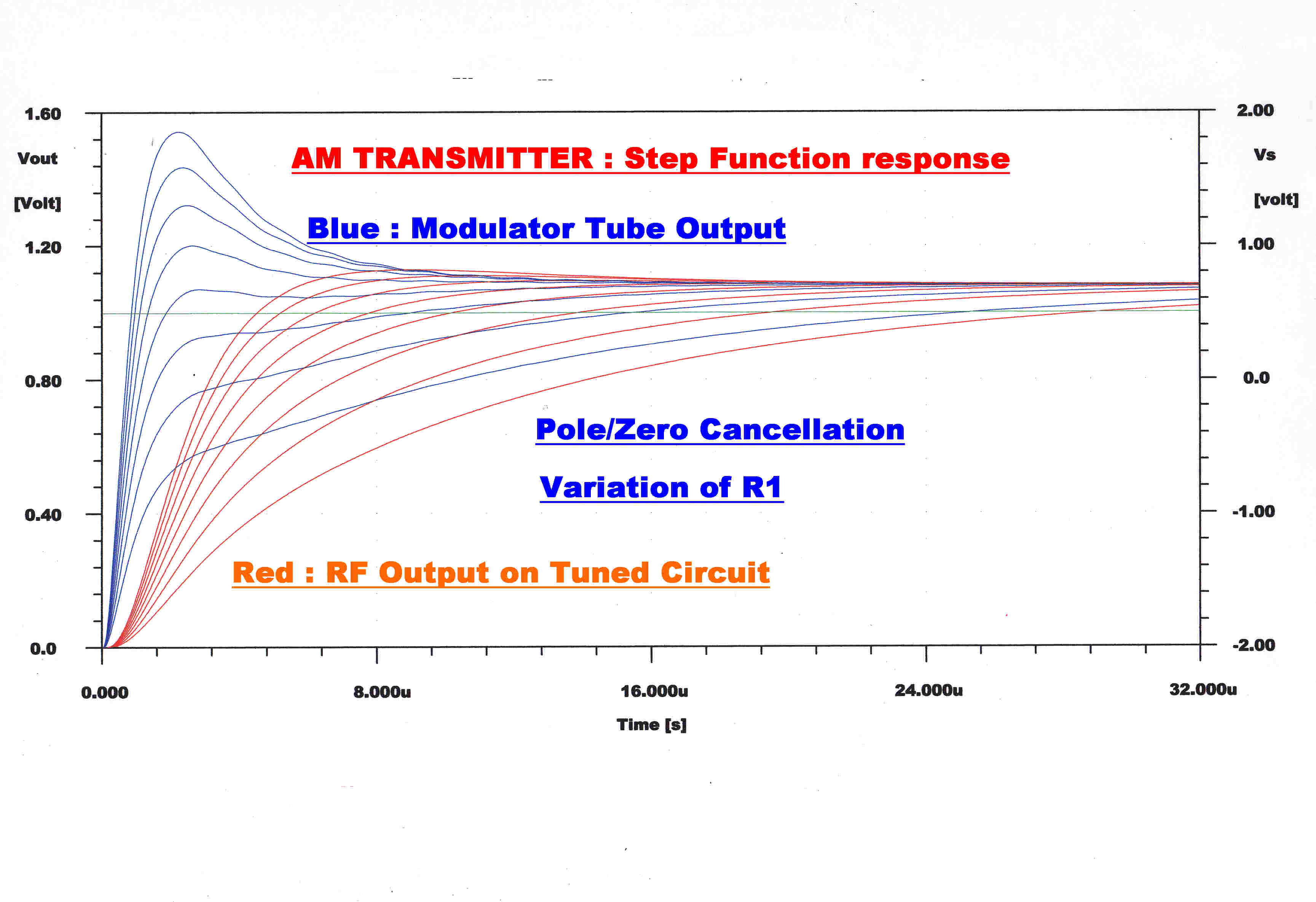
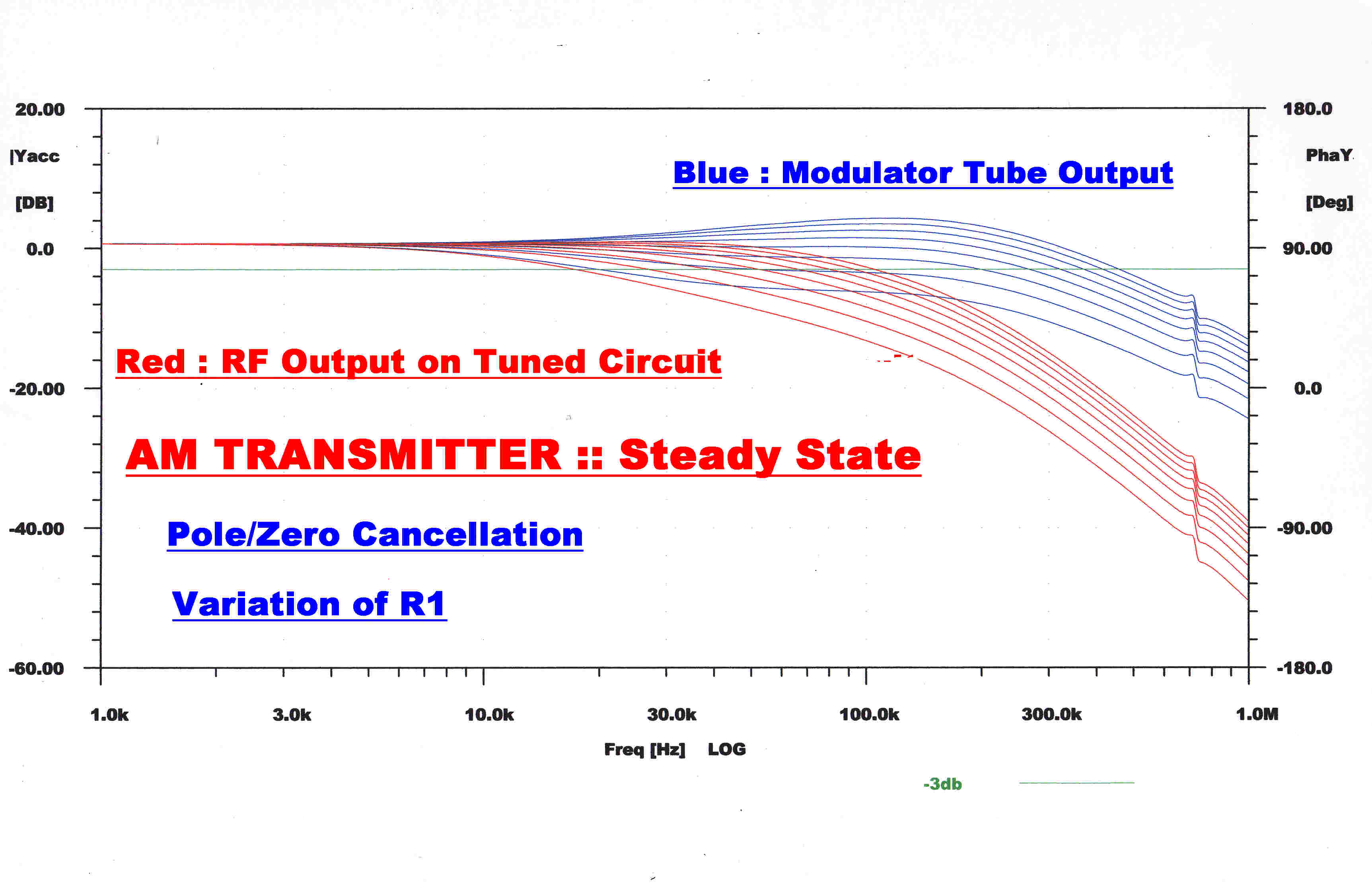
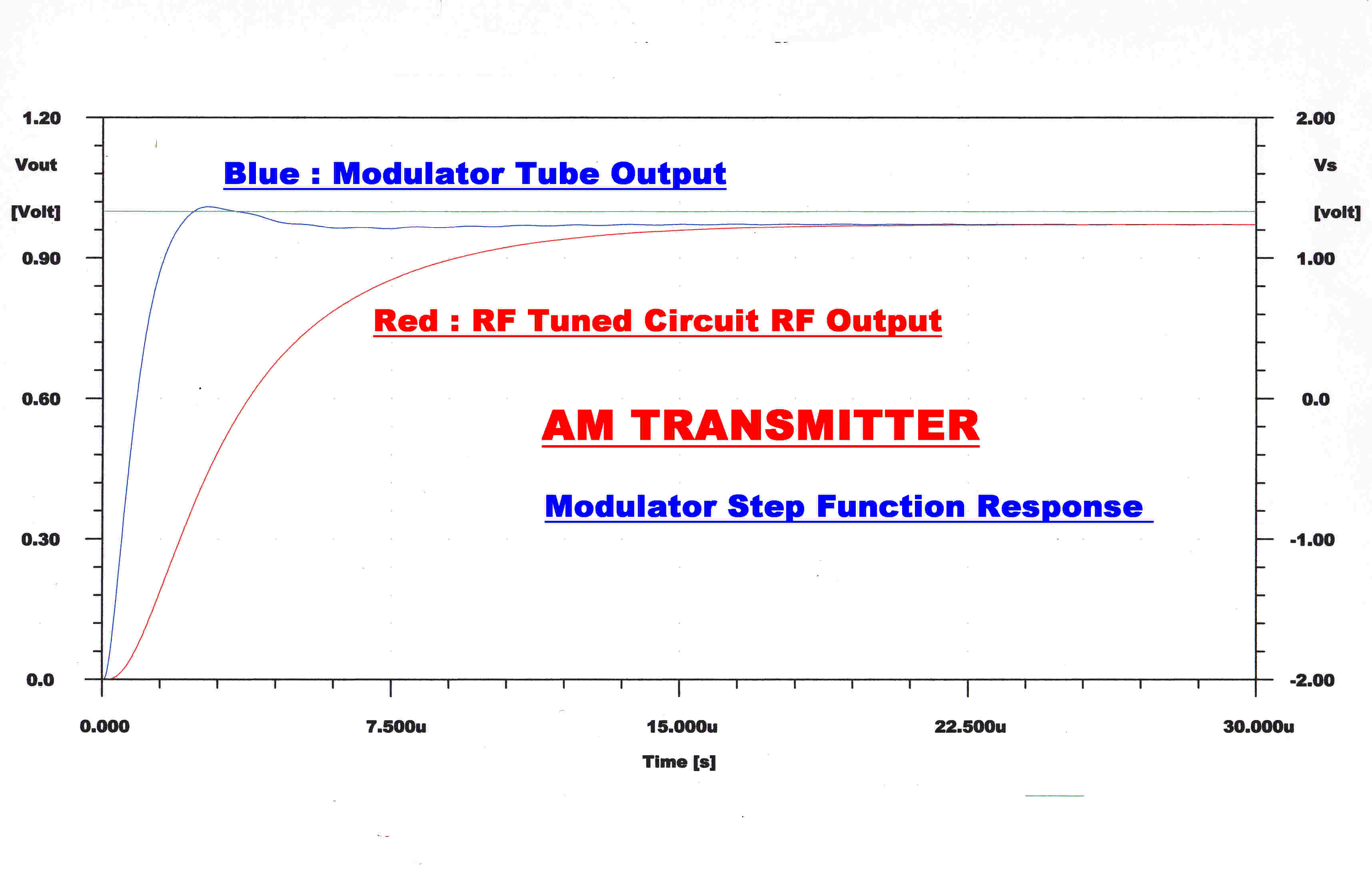
The change in steady state and step function response is shown as R1 changes to change
τc.
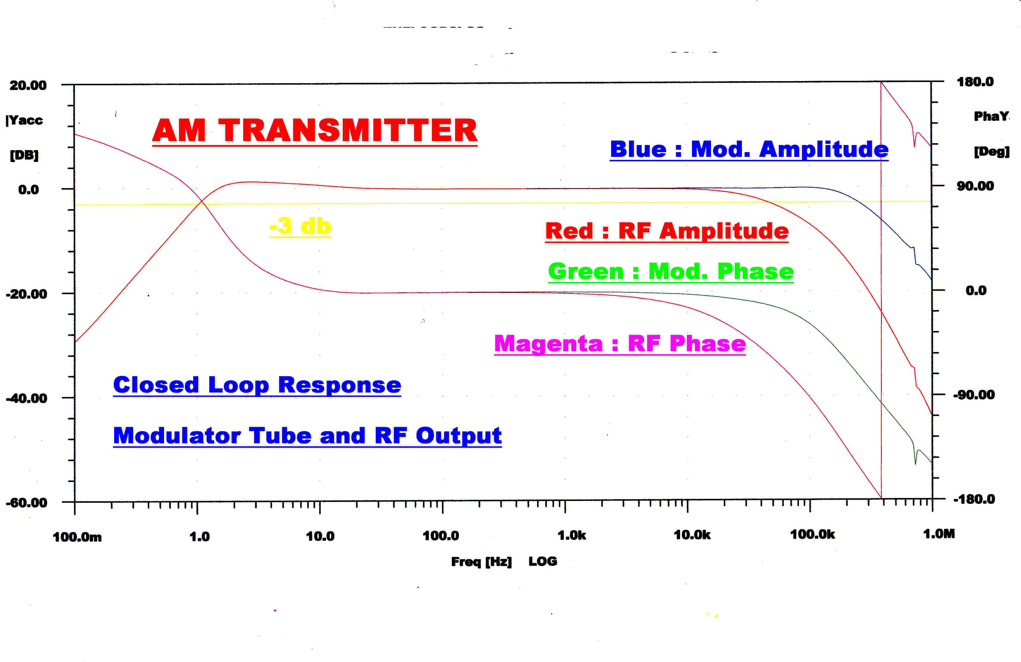
The output from the modulator is shown in blue and the output from the RF tuned
circuit in the plate is shown in red.
The transfer function for the modulation of the tuned circuit is given by:-
Ytc(p) = 1/( 1 + τtcp ) where:-
τtc = 1/2B where the total bandwidth, B, of the tuned circuit is given by:-
B = fc/Q
where fc is the carrier frequency and Q is the Q of the tuned circuit.
Here B ≈ 40KHz.
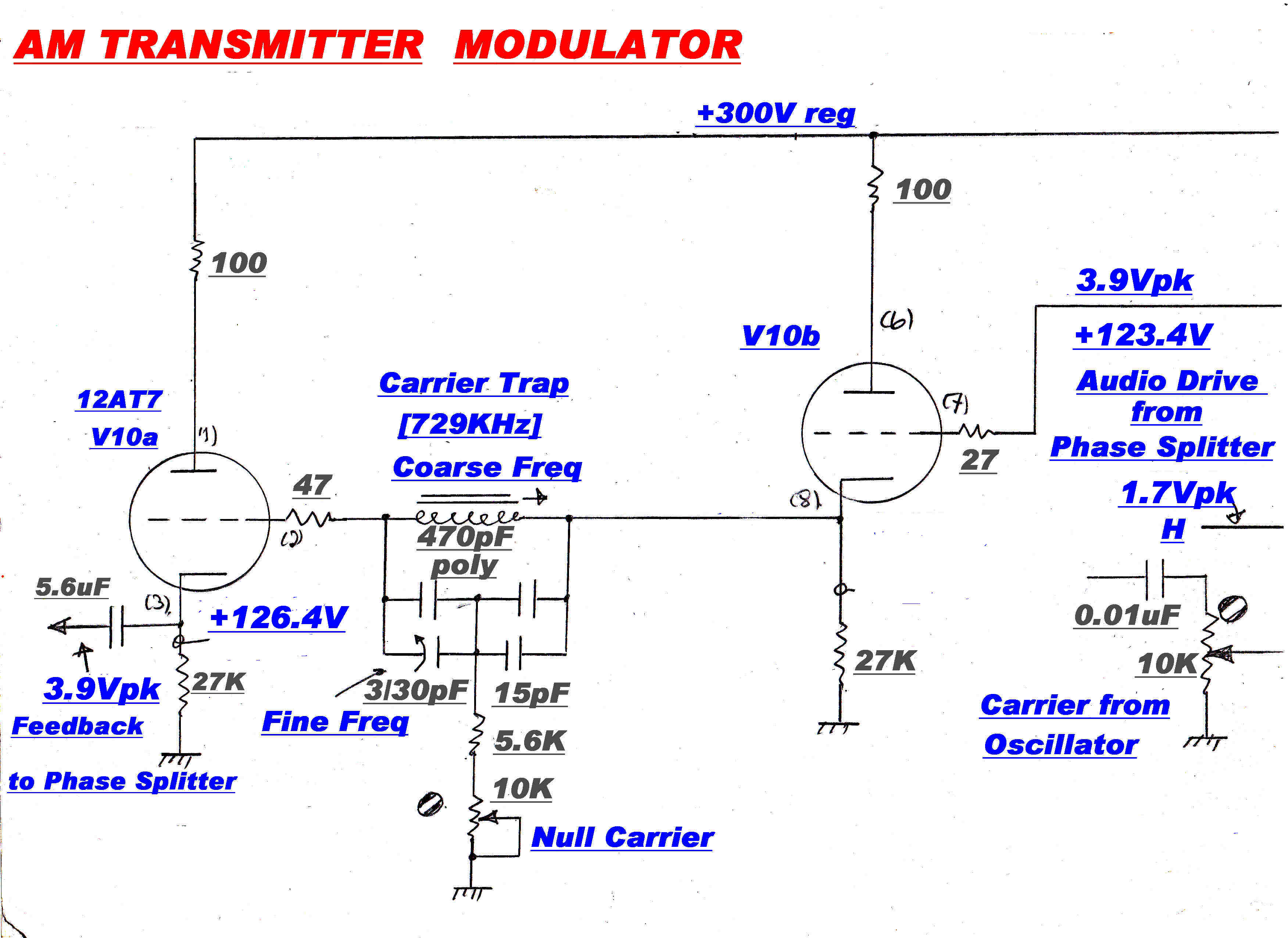
 Carrier Trap
To reduce the level of carrier in the feedback loop a trap is placed between V1 and
V2. This tends to decrease the stability margin in the loop. To increase the gain
margin a shelf is introduced by the secondary fedback loop R5, R6,
R7, C5. This shelf starts at 50KHz. and ends at 150KHz., thus improving
the gain margin by 3.
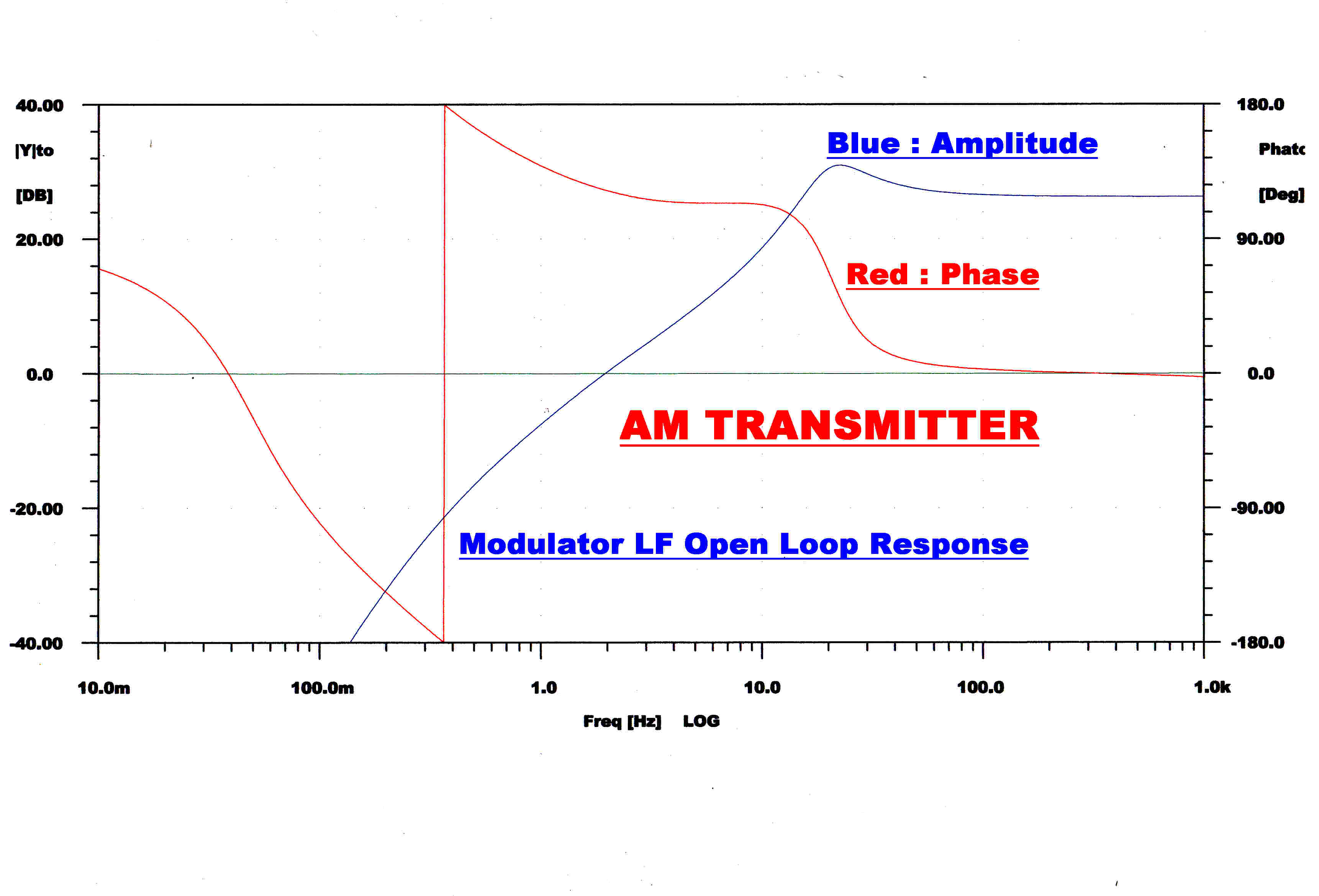
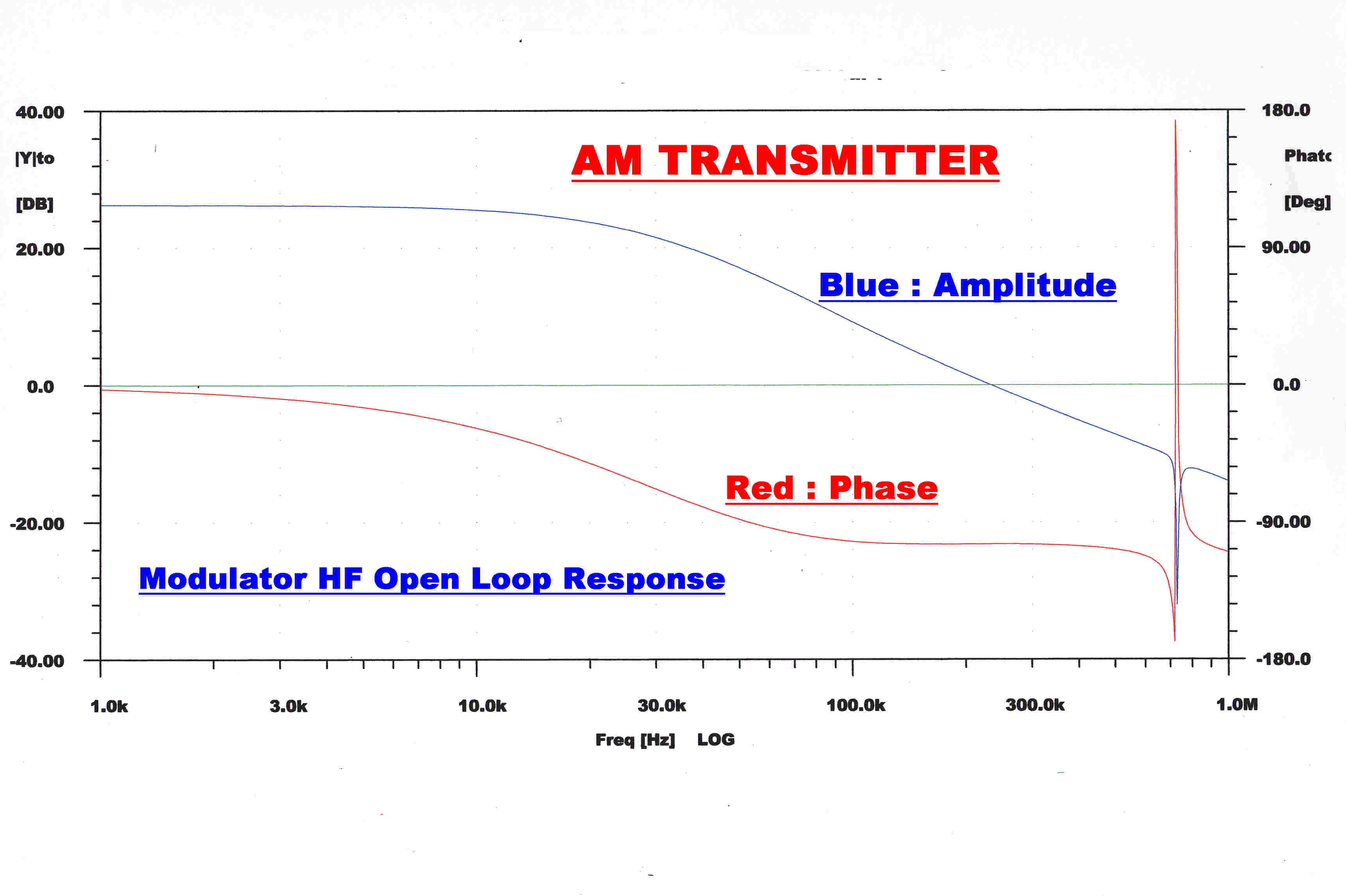
The high and low frequency open loop transfer functions are shown.
The increase in slope between 50KHz. and 150KHz. can be seen.
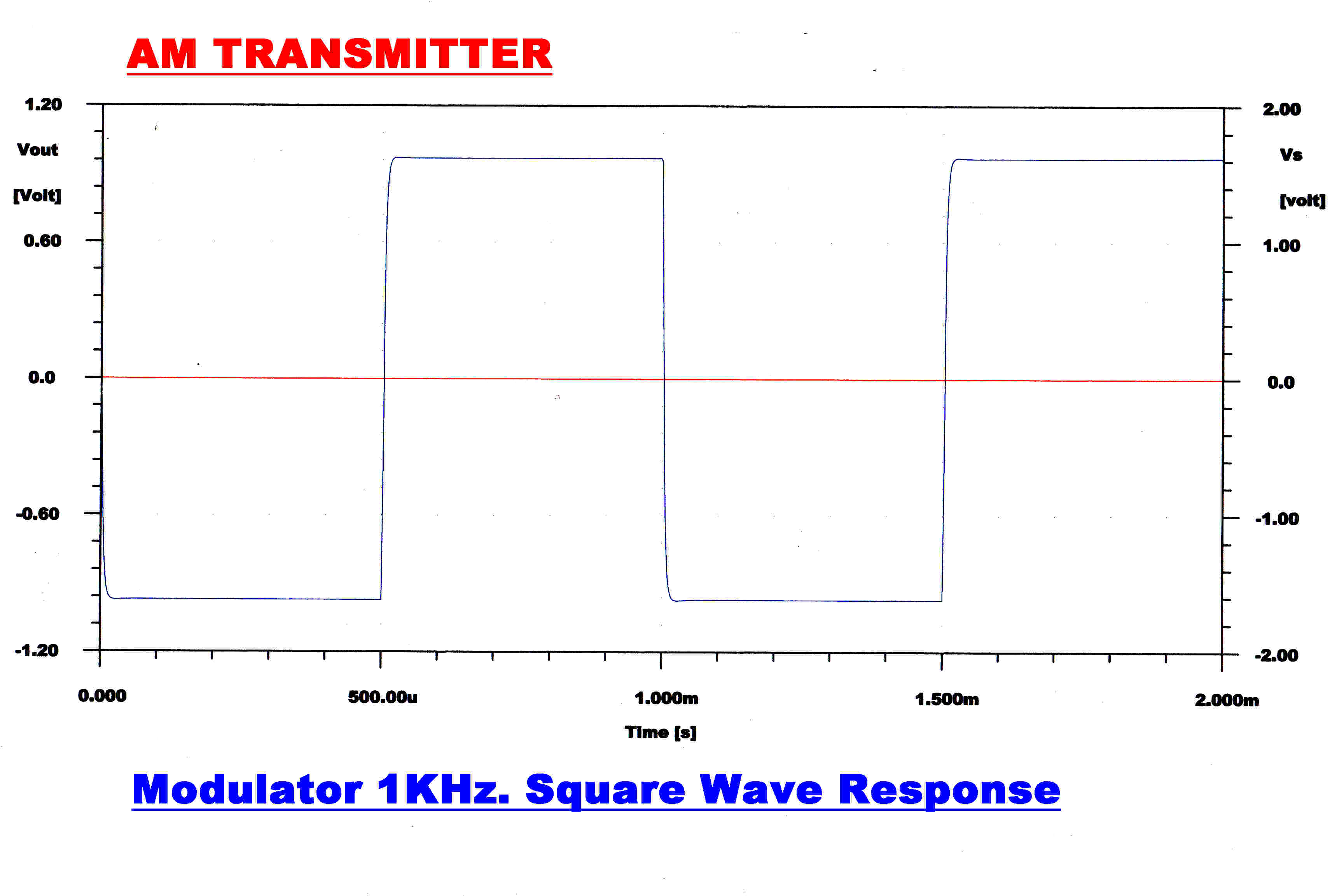
The closed loop steady state, step function and 1KHz. square
wave responses are shown below.
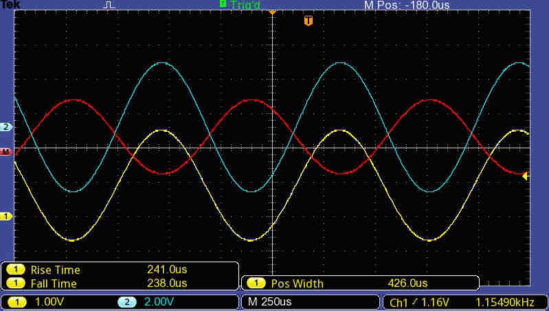
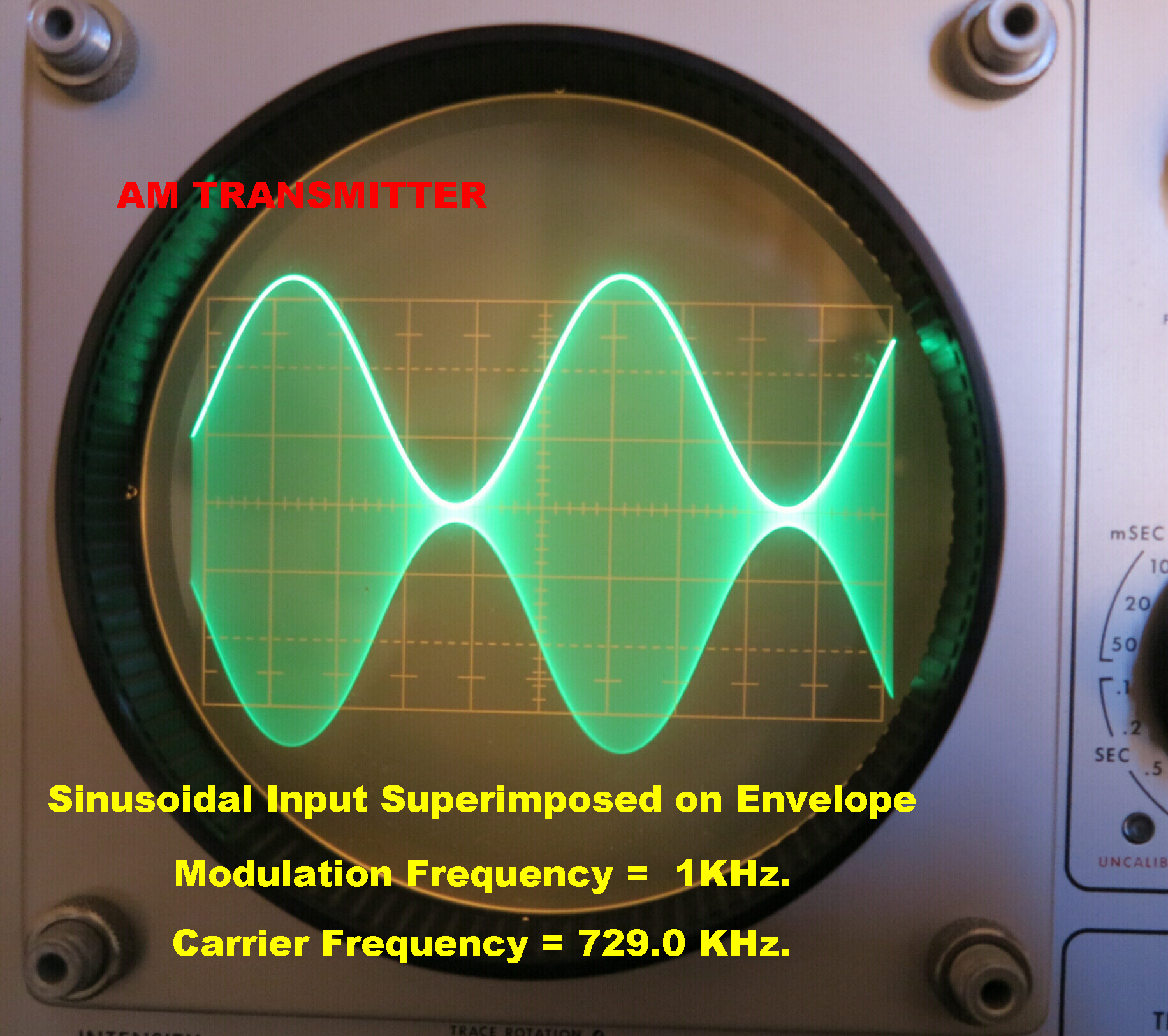
Some key waveforms.
1KHz square wave input with 100% modulation.
|
|
|
|
|
Yellow:Deflecting Voltage on Plate 1 |
Yellow: Voltage on Deflecting Plate 1 |
Top: Voltage on Deflecting Plate 1 |
In the development of this transmitter two beam tubes type 6AR8 were used. Both were centered -
that is the deflection plate currents were equal with no deflecting voltage. Subsequent experience with another
20 beam deflection tubes of types 6AR8 and 6JH8 showed that a significant fraction had unequal plate currents
for no deflecting voltage.
It is imperative that the modulator be modified to incorporate a pre-adjusted centering system.
Note: The beam deflection tubes were designed as colour sub-carrier product demodulators in colour TV receivers.
Here the deflection plates were hard driven from one side to the other, so lack of initial balance was
of no consequence. The tolerancing is therefore not given in the tube data.
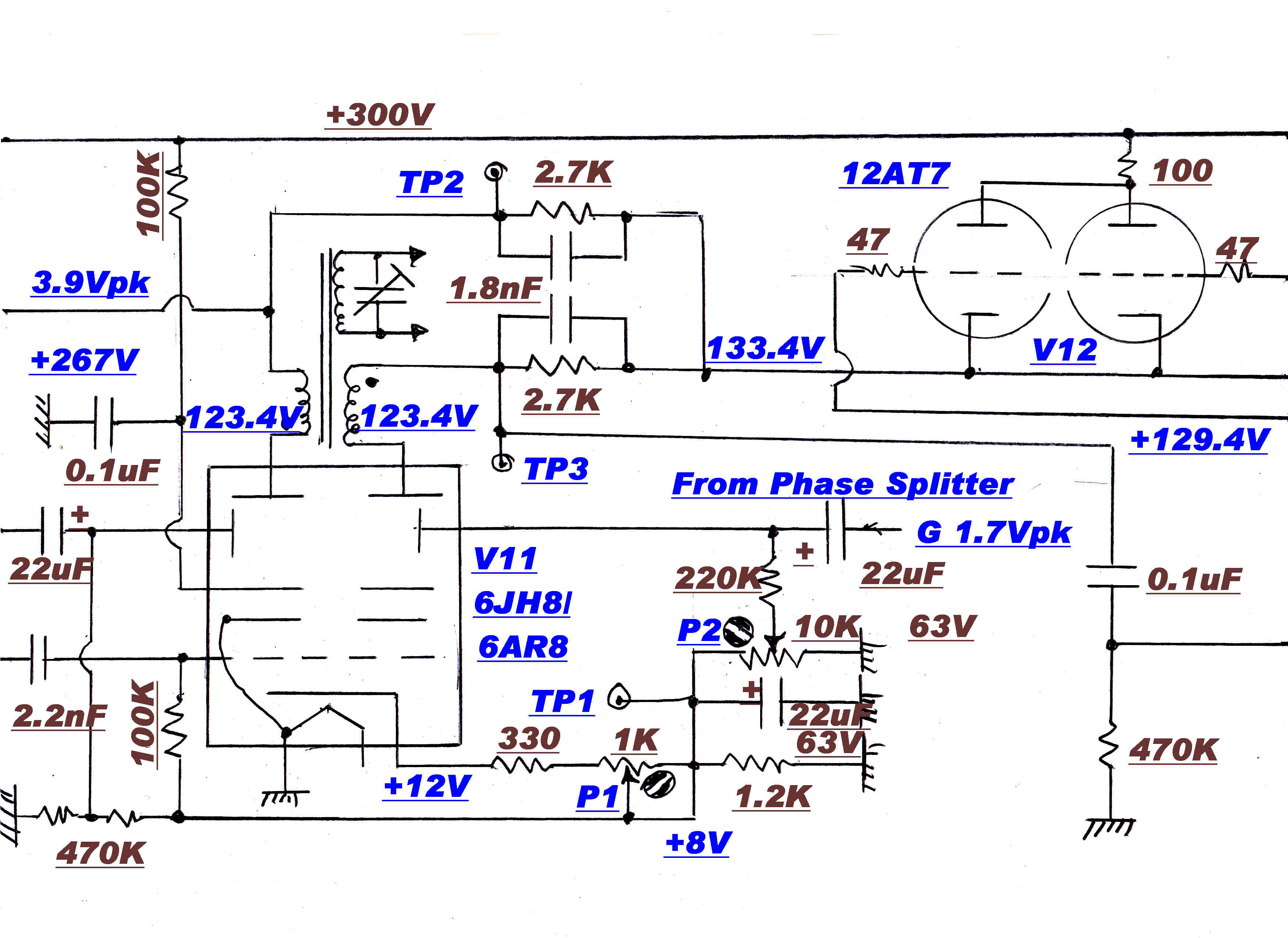
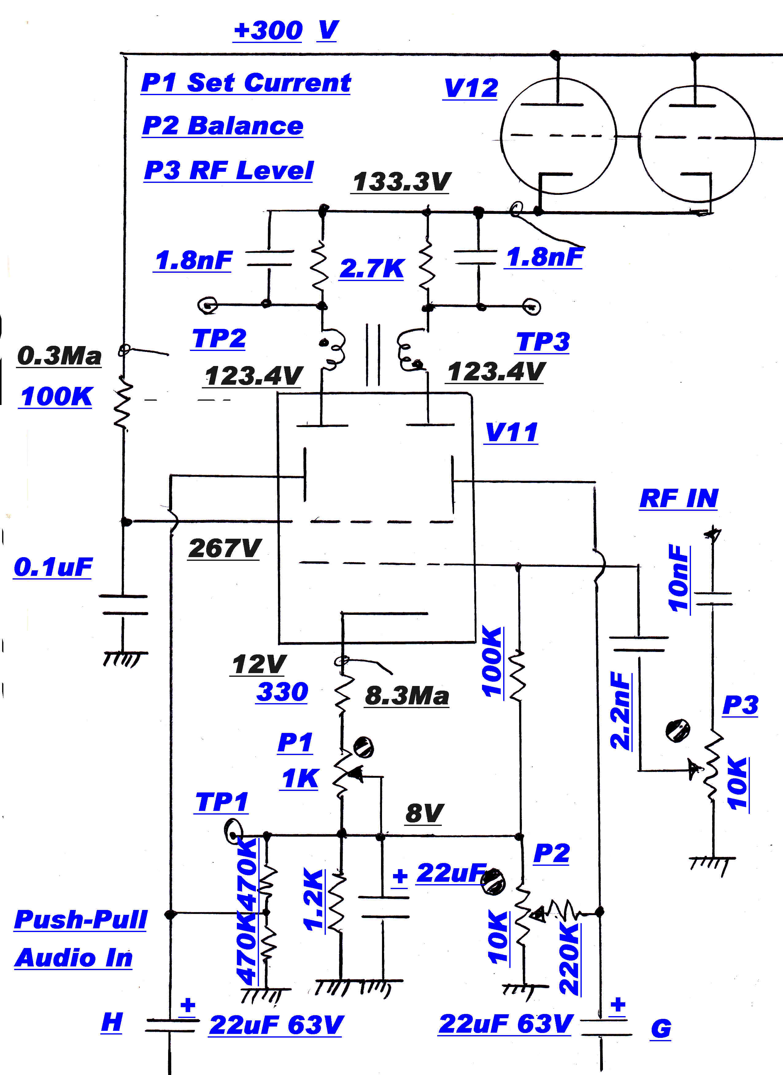 The balance circuit added to the beam deflection modulator is shown on the right.
Provision is made for:-
[1] Setting the total beam current to 8Ma -- P1
[2] Centering the beam currents -- P2
[3] Adjusting the RF drive -- P3
PROCEDURE
[A] The RF drive is set to zero with pot. P3
[B] The total plate current is set to 8Ma by adjusting P2 until the voltage on TP1 is 8 volts.
[C] The deflection tube is balanced by setting P2 until the DC voltages on TP2 and TP3 are equal.
[D] P3 is adjusted to give a peak RF output at 100% modulation of about 400mV at the output terminals.
Design Note:-
AC coupling is used to add the DC offset voltage to the deflecting voltage.
This adds another low frequency pole to the feedback loop. The cutoff frequency caused by this pole must be
well below the unity gain frequency of the loop. This is determined by the 22uF coupling capacitors.
Smaller capacitors down to 2.2uF would fulfill the condition, but 22uF capacitors were used because
of their availability.
The larger capacitors have one disadvantage : the balance preset adjustmant takes longer to settle after a change
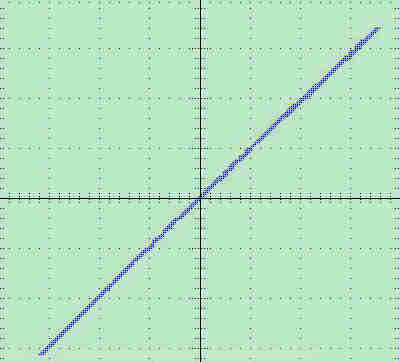
The following oscillograms illustrate the linearity of the beam tube deflection.
All oscillograms were taken with 100% modulation on the transmitter.
|
|
|
|
Yellow:Deflecting Voltage on Plate 1 |
Plot of deflection current versus deflecting voltage for beam deflection tube. |
Plot of deflection current against voltage at the input terminals of the transmitter. |
The modulation envelope and the audio input coincide.
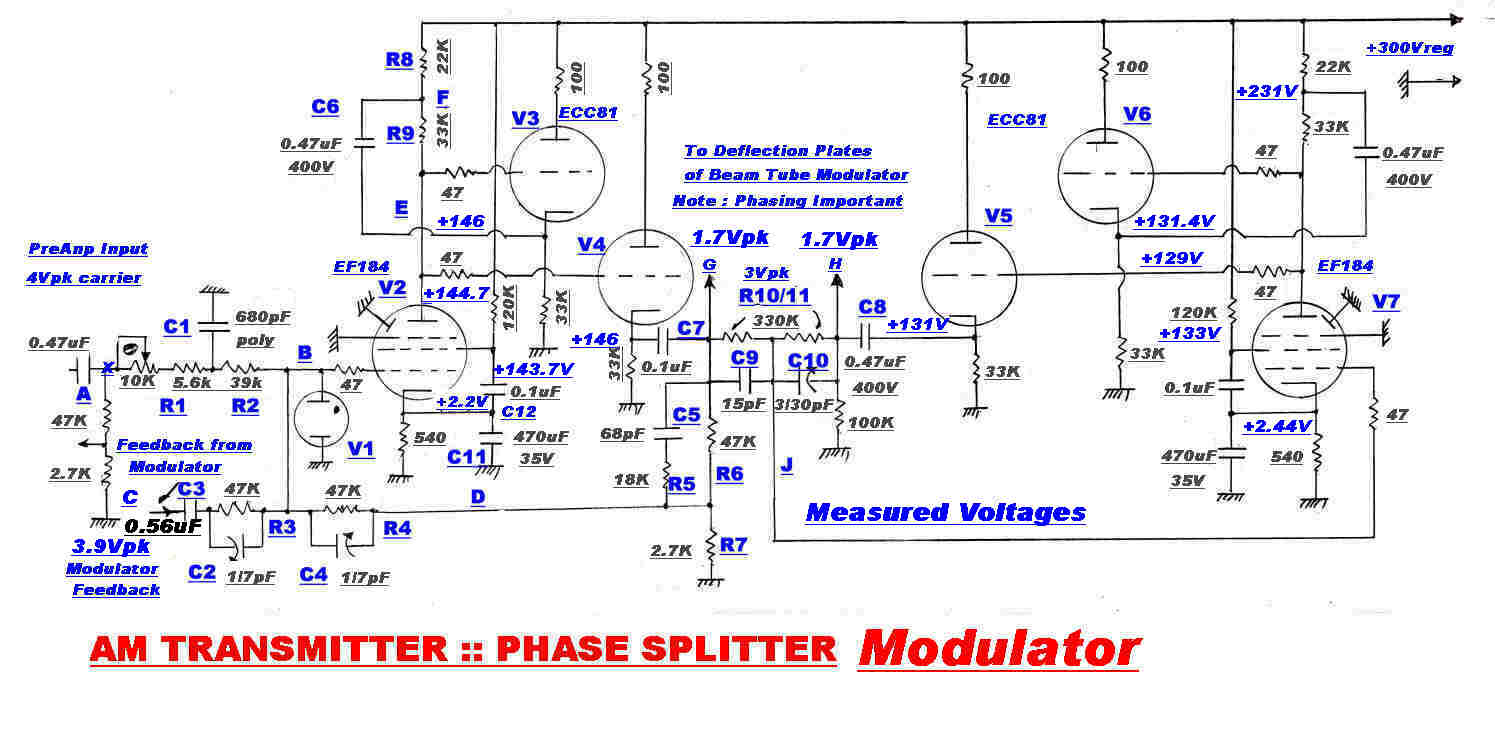 The detailed circuit of the modulator is shown above.
V2,V3,V4 and V5,V6,V7 form two operational amplifiers.
Gain is increased by boot-strapping through V3 and V6. This increases the effective dynamic
load on the EF184 pentodes and reduces the HF turnover frequency to about 8KHz. The low frequency
turnover determined by the time constant (C6 R8) occurs at about 300Hz. The final low
frequency gain is determined by screen and cathode degeneration.
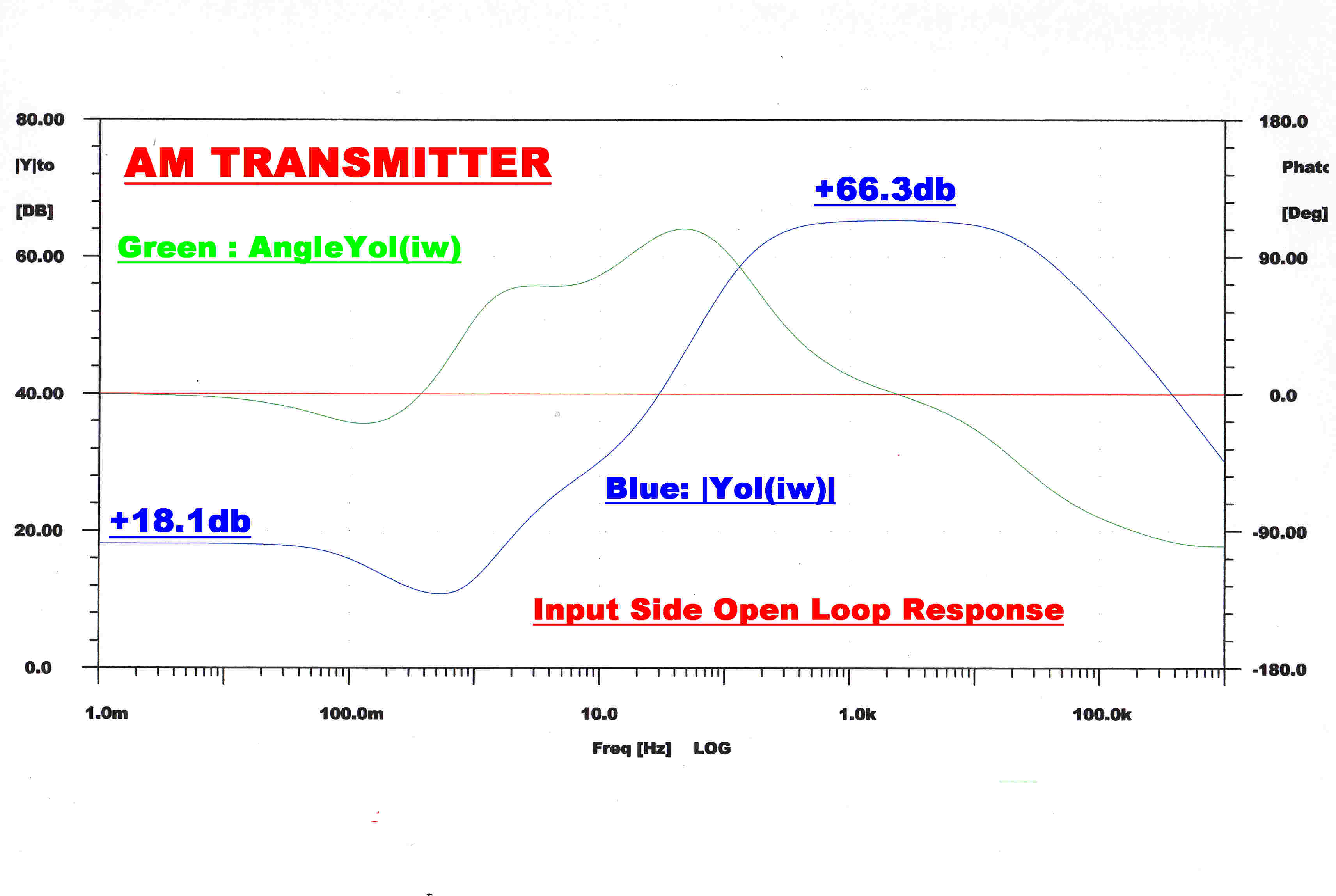
The open loop gain of the amplifier is shown on the right.
 Phase reversal occurs in the RHS operational amplifier.
R10-C9 is the front impedance and R11-C10 is the feedback network.
 The high frequency closed loop response ( both steady state and transient ) of the phase
splitter with and without the shelf network is shown on the right.
The high frequency closed loop response ( both steady state and transient ) of the phase
splitter with and without the shelf network is shown on the right.
The dominant and stabilising pole in the high frequency phase splitter loop is generated by
the load on the EF184 pentodes and capacity to earth.
The 50KHz to 150KHz shelf to give extra gain margin in the overall loop is generated by R5-C5.
Referring to the shelf generation in the phase splitter circuit:-
Let Ra = R6 :: Rb = R7 and R4 in parallel :: Rf = R5 :: Cf = C5 :: fb = bottom shelf frequency
and ft = top shelf frequency. We get:-
Rf = Ra( 1 - (ft/fb)( Rb/( Ra + Rb ) ) )/( ft/fb - 1 )
Cf = 1/( 2Πfb( Ra + Rb ))
Here ft = 150KHz. :: fb = 50KHz. :: Ra = 47k :: Rb = 2.5533K so:-
Rf = 19.867k :: Cf = 64.23pF.
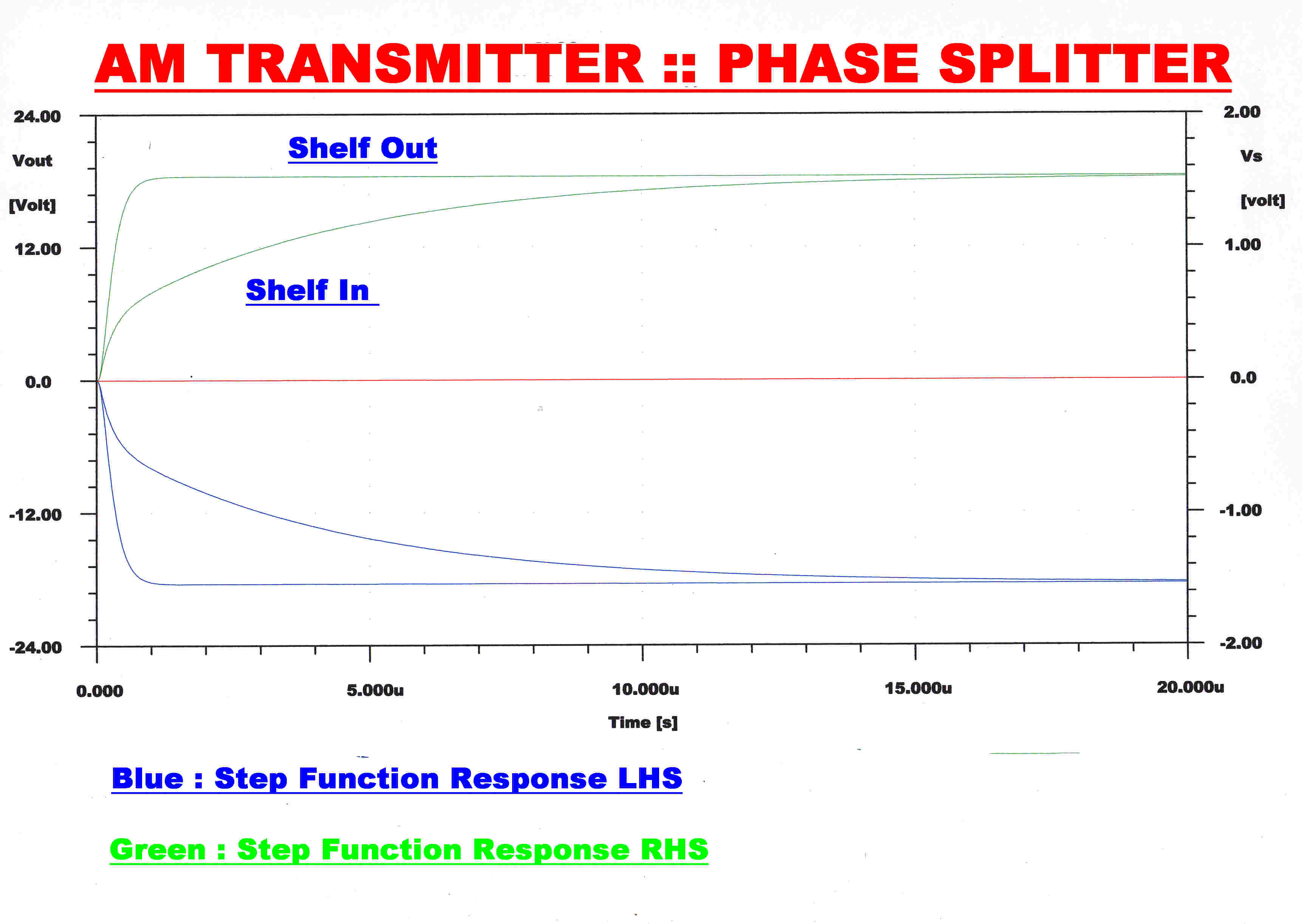
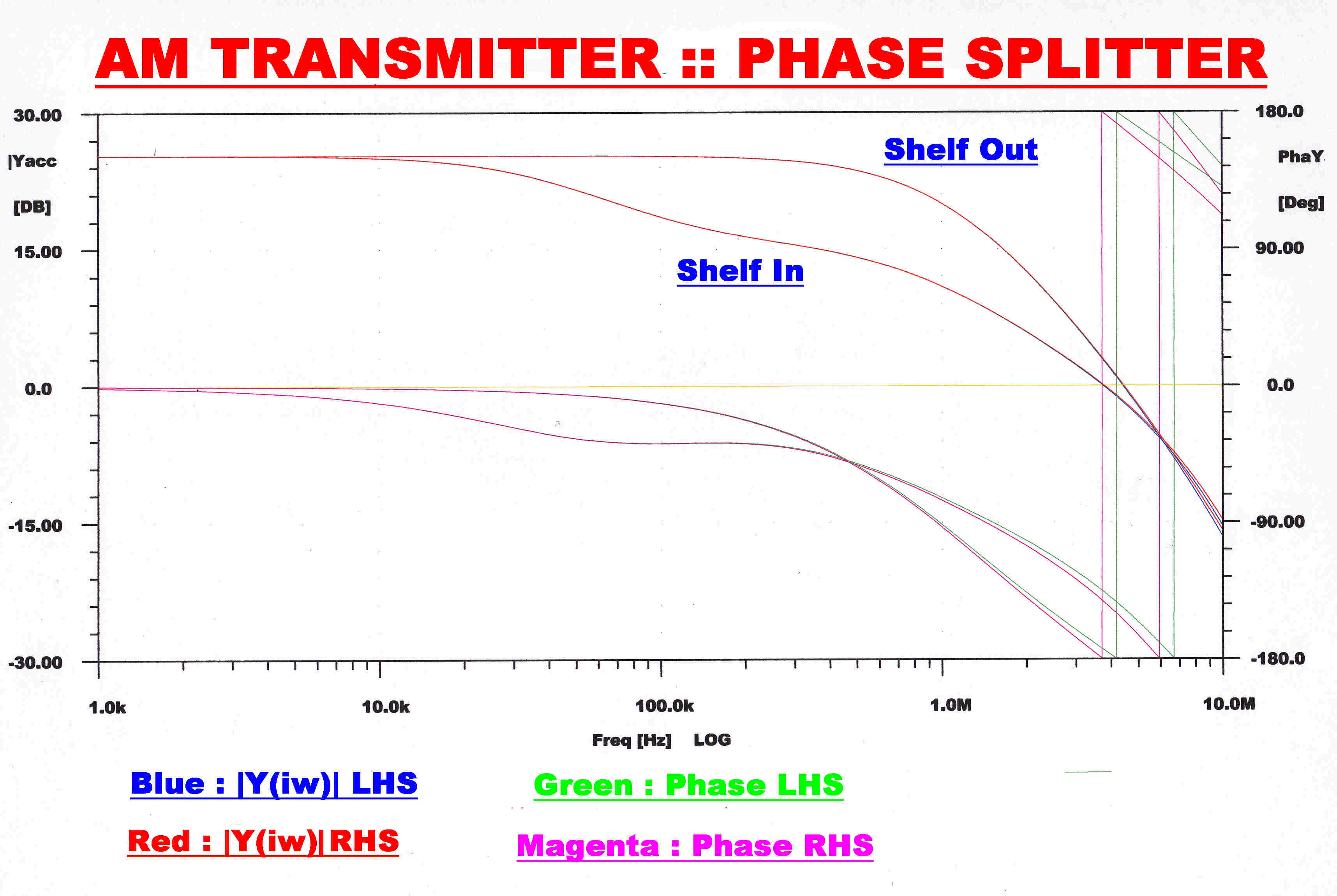
 The closed loop low frequency response of both sides of the phase splitter is shown opposite.
They track down to about 0.1Hz where the RHS has more attenuation and phase shift because
it has one more low frequency coupling network ( C8) than the LHS.
The closed loop low frequency response of both sides of the phase splitter is shown opposite.
They track down to about 0.1Hz where the RHS has more attenuation and phase shift because
it has one more low frequency coupling network ( C8) than the LHS.
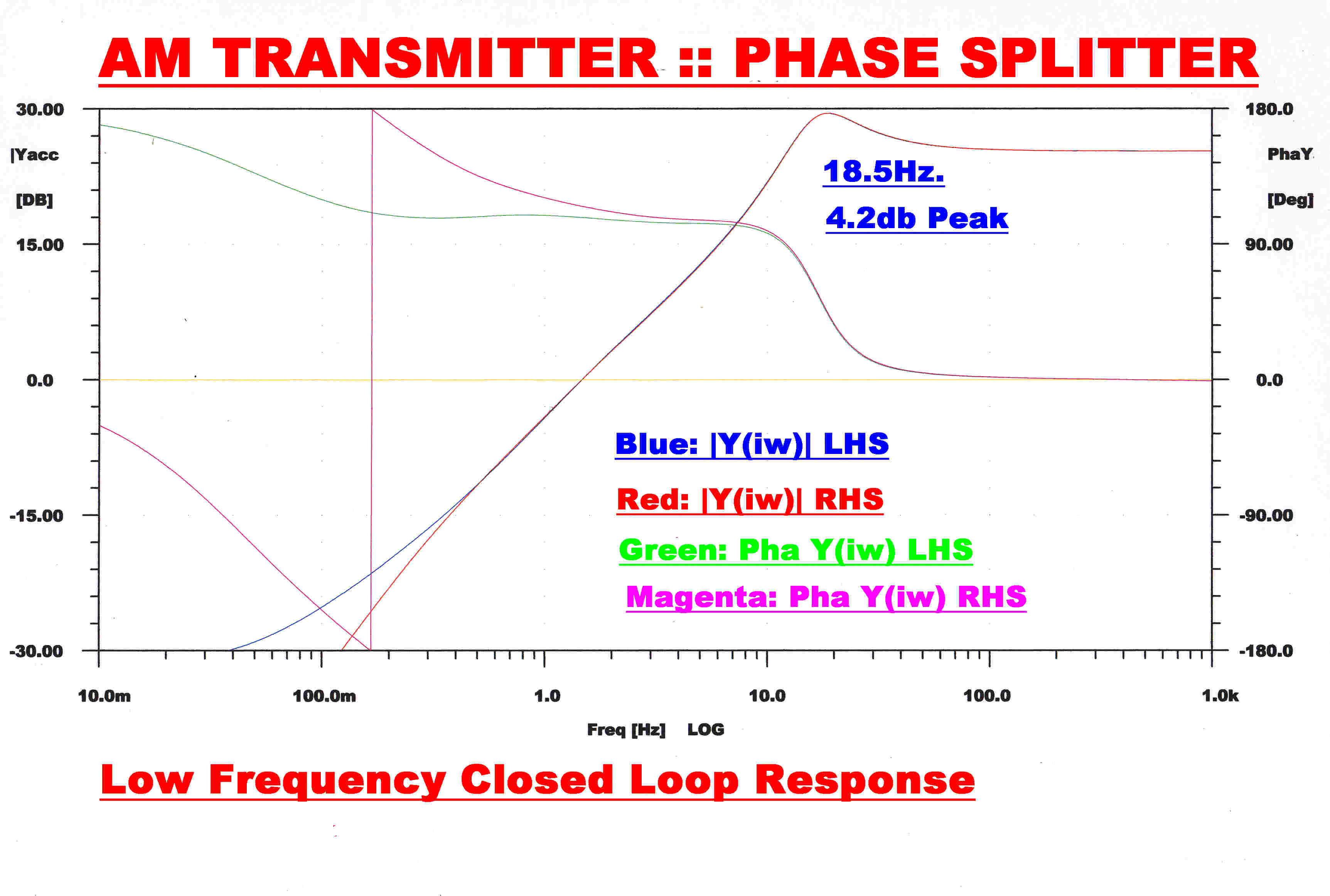
The open loop low frequency transfer function is fourth order:-
Y(p) = [(1 + Tkz p)/(1 + Tkp p)]
X[(1 + Tsz p)/(1 + Tsp p)]
X[(1 + Tbz p)/(1 + Tbp p)]
X[ Tcz p/(1 + Tcp p)]
Where Tkz, Tkp ;Tsz, Tsp ;Tbz, Tbp
are zeros and poles on the real axis due to the cathode decoupling, the screen decoupling, and
the anode bootstrapping.
There is a pole at the orogin, Tcz, due to the AC coupling : C7 and ( R6 + R7)
The low frequency open loop gain due to boot strapping turns over at about 300Hz. to ensure low frequency
closed loop stability. The low frequency response has a 4.2 db peak at 18.5 Hz.. This is of no
consequence, since it is covered by the modulator feedback, giving a peak of about 1.3db between 1 and 2 Hz.
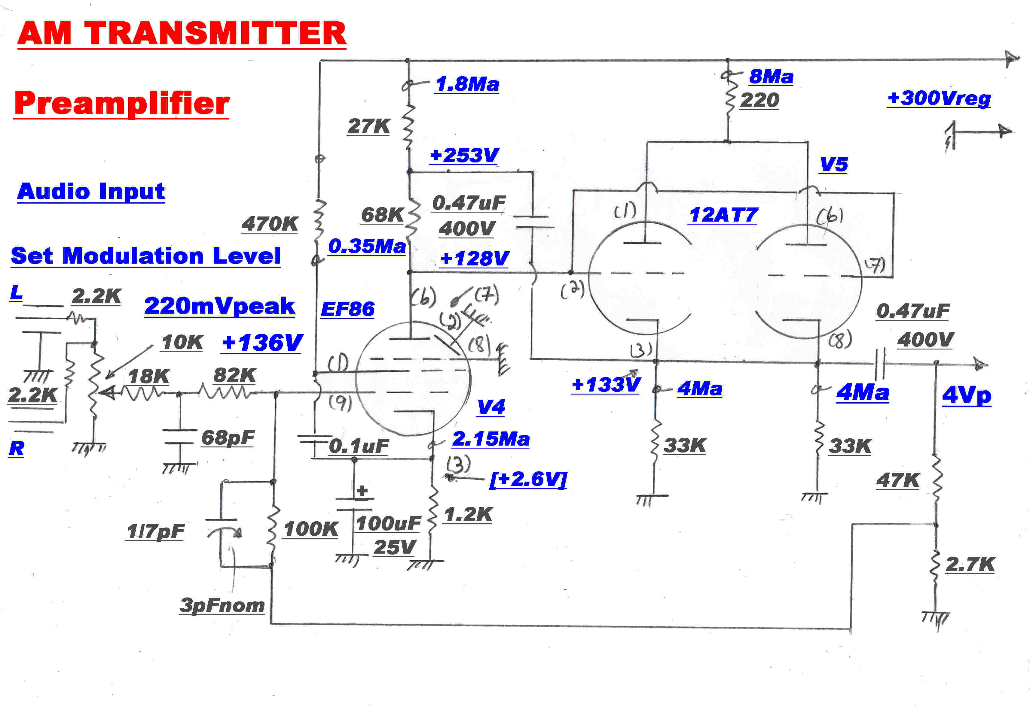 The circuit of the audio preamplifier is shown on the right.
The design uses the same bootstrapping technique used in the phasesplitter.
The input pentode is an EF86 - a tube designed for low noise and hum.
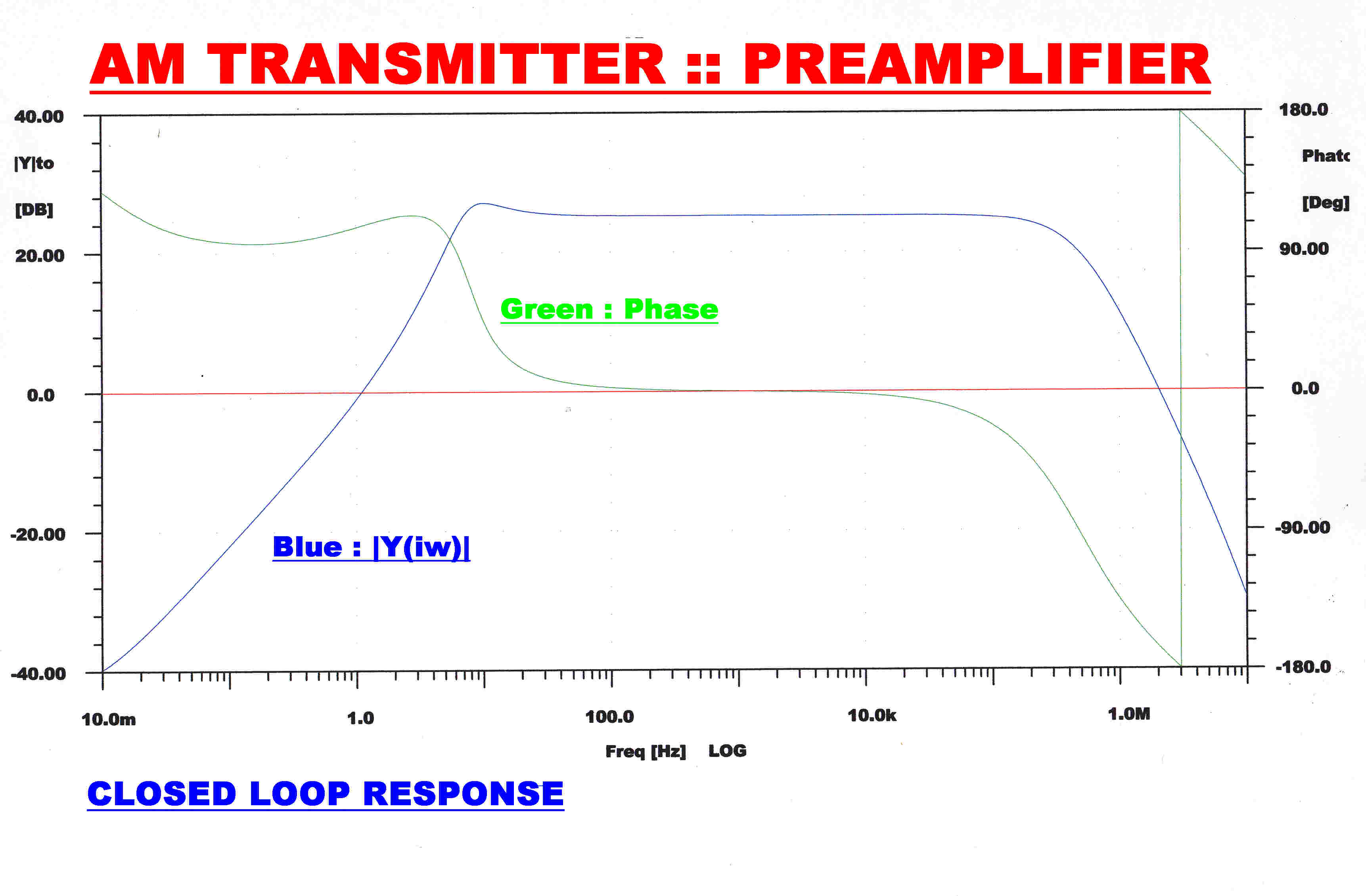
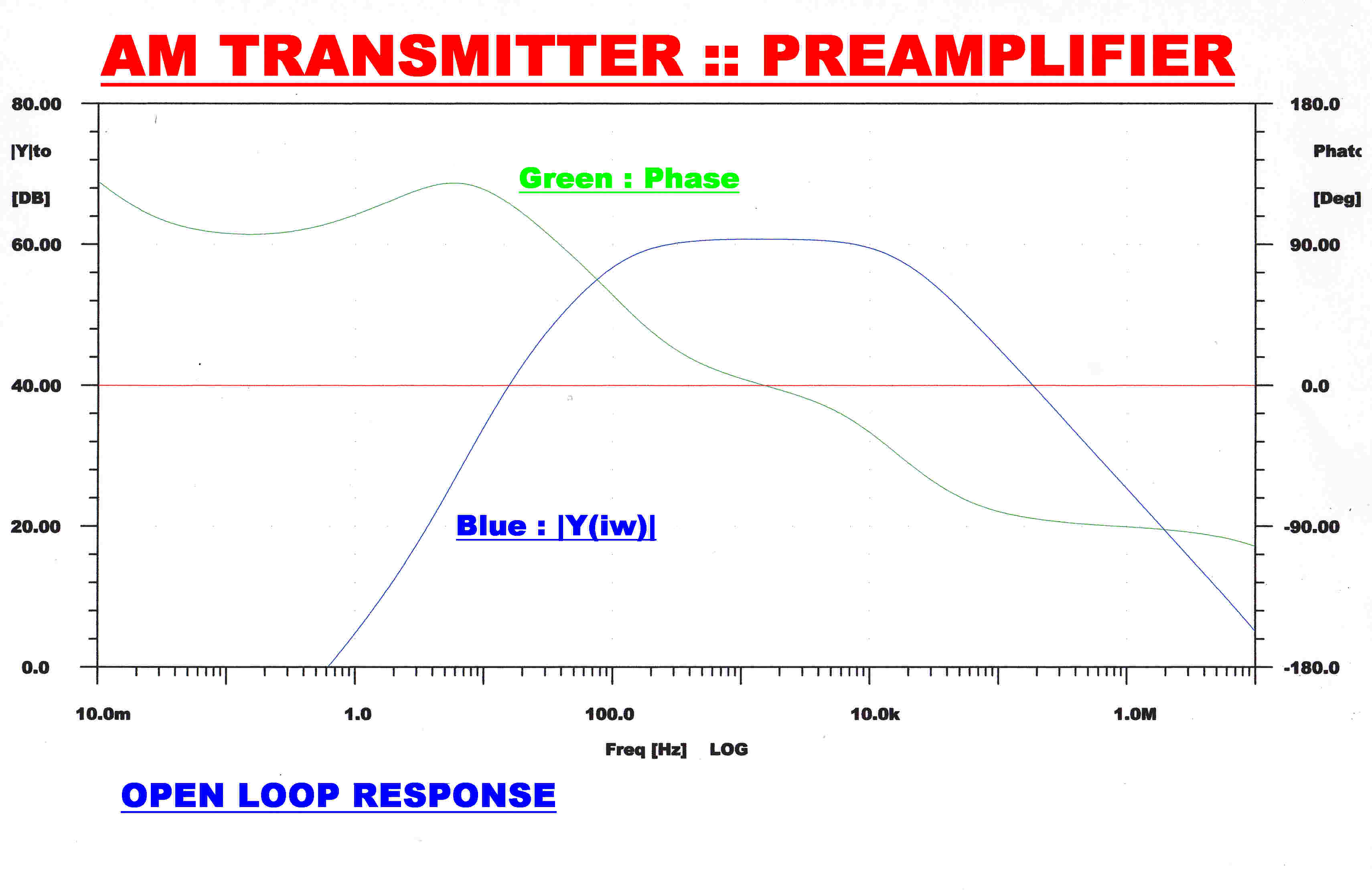 The open loop and closed loop response of the preamplifier is shown on the right.
A single pole RC filter on the input attenuates any RF pickup by the audio chain.
This has a 3db frequeny of about 150KHz.
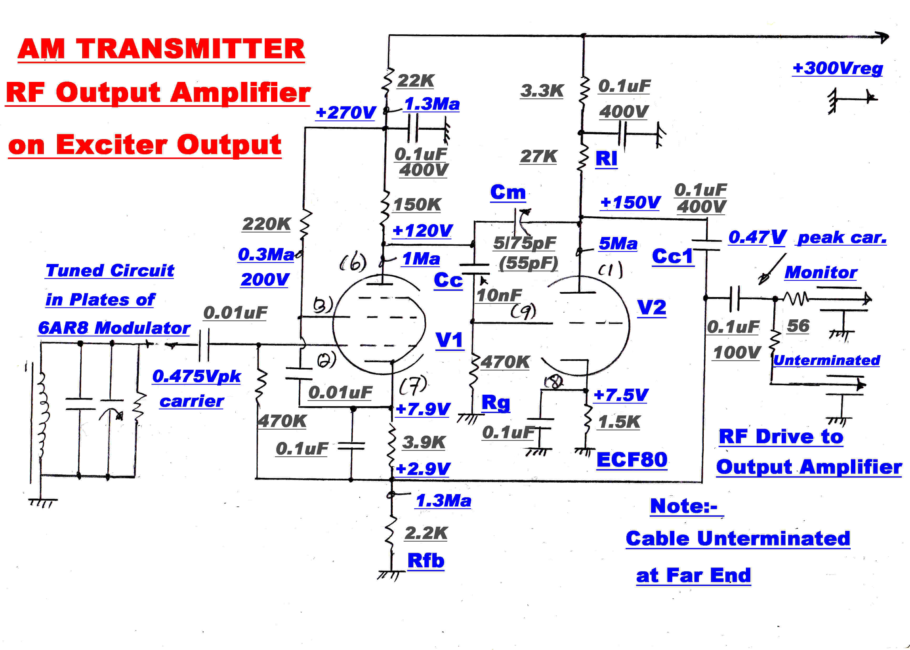
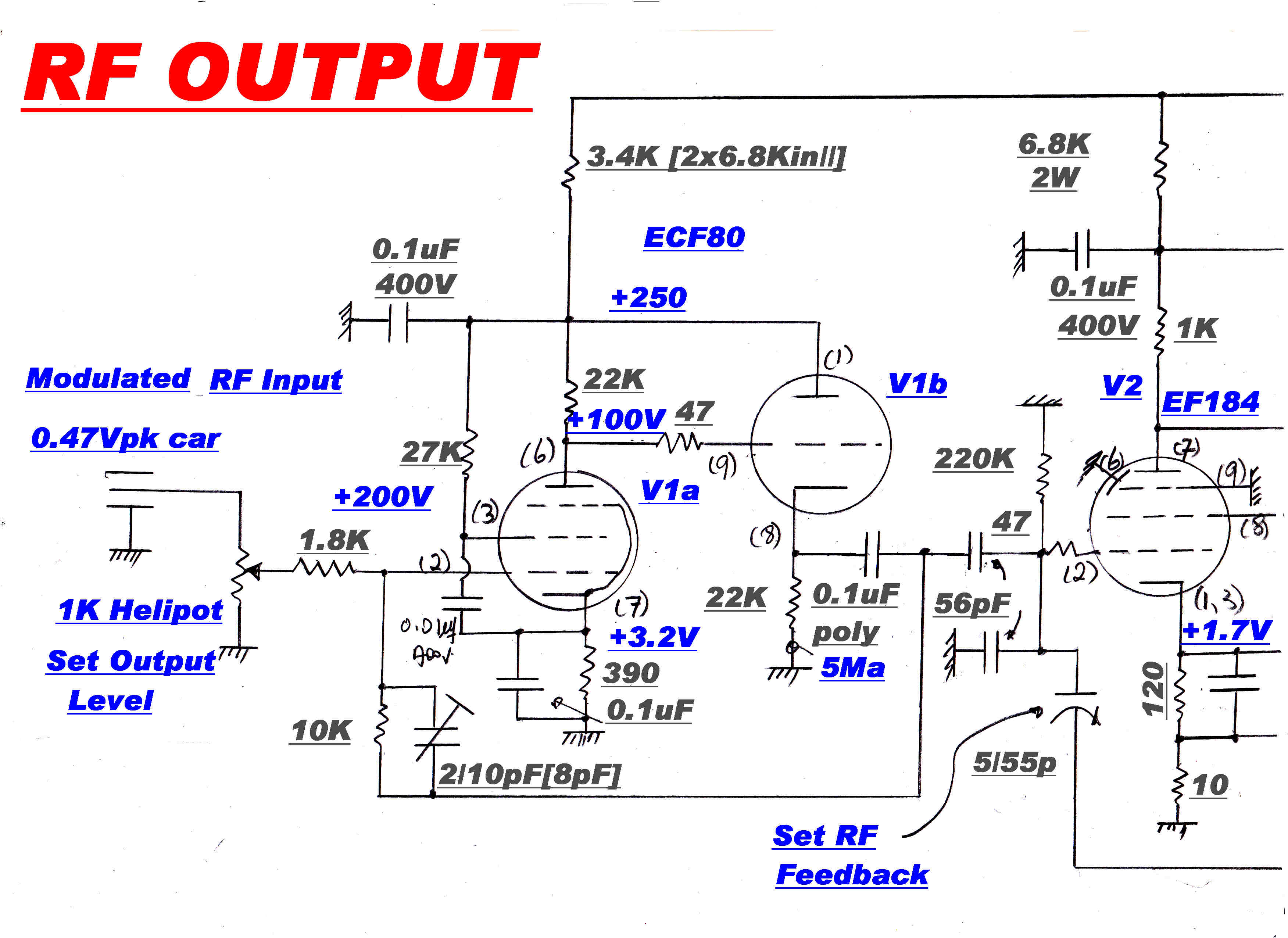
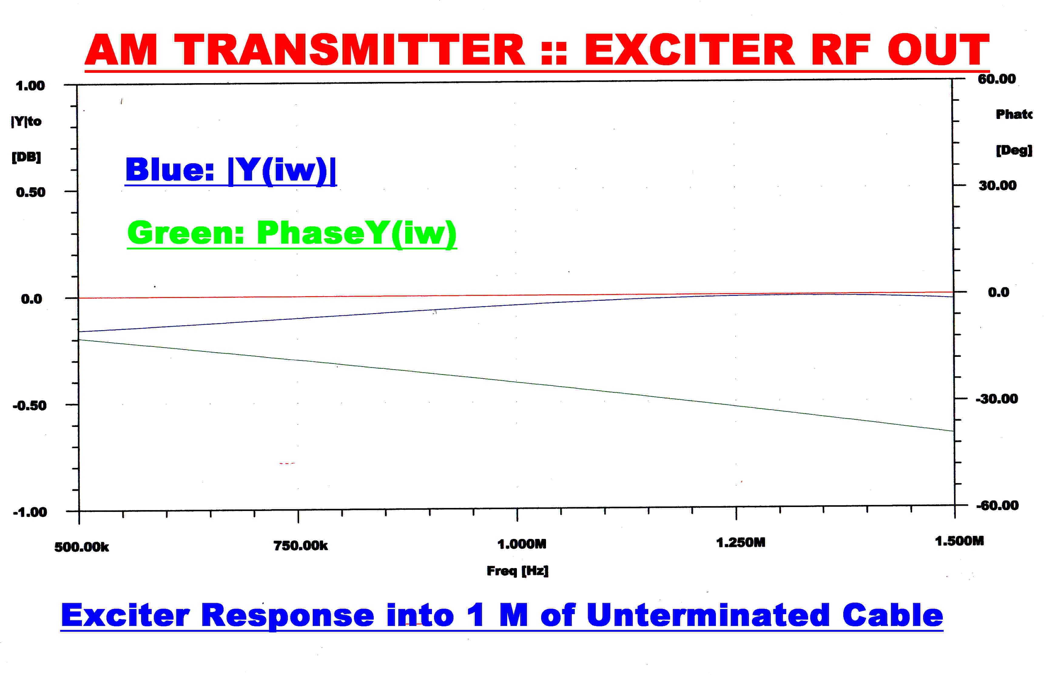 The buffer RF output amplifier drives about 1 M of unterminated cable connecting the
exciter with the power output amplifier. The requirements are:-
The buffer RF output amplifier drives about 1 M of unterminated cable connecting the
exciter with the power output amplifier. The requirements are:-
(1)Very low distortion
(2)Flat amplitude response across any AM channel (here 80KHz. wide).
(3)Phase linearity across the channel.
V2 acts as a Miller integrator with Cm the Miller feedback capacitor.
V1 provides constant current drive for the integrator.
The steady state response of the amplifier across the broadcast band is shown on the left.
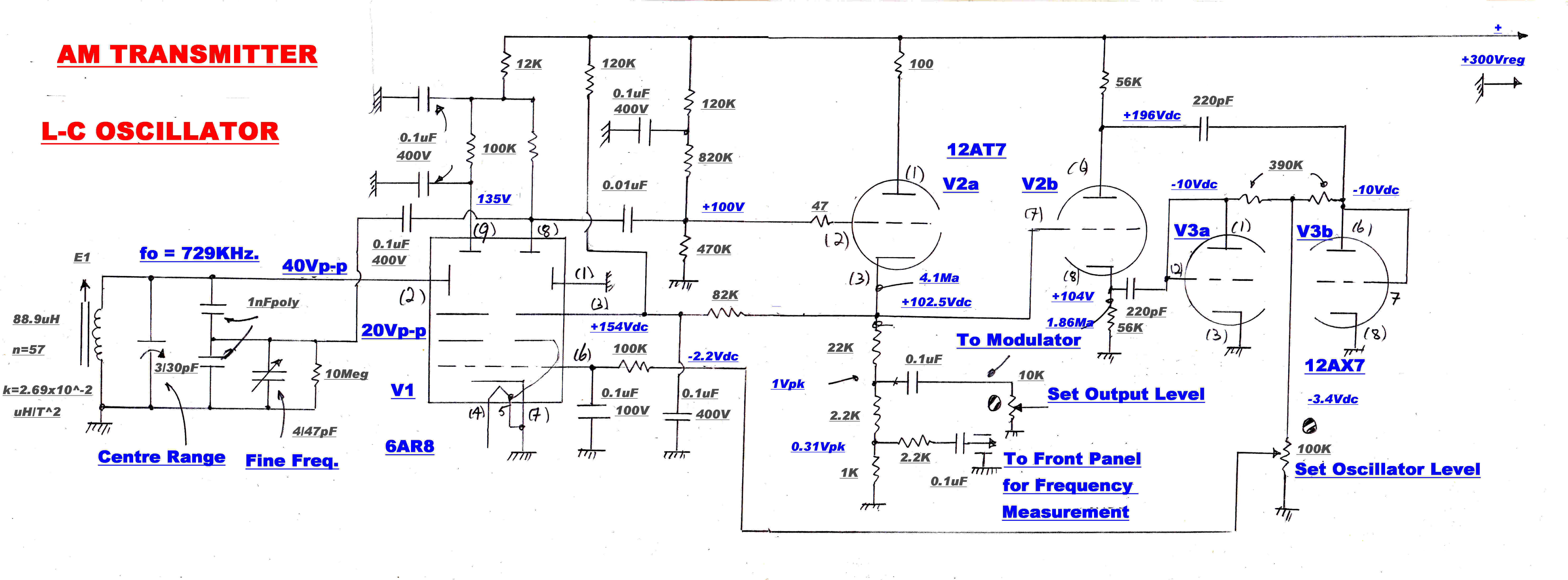
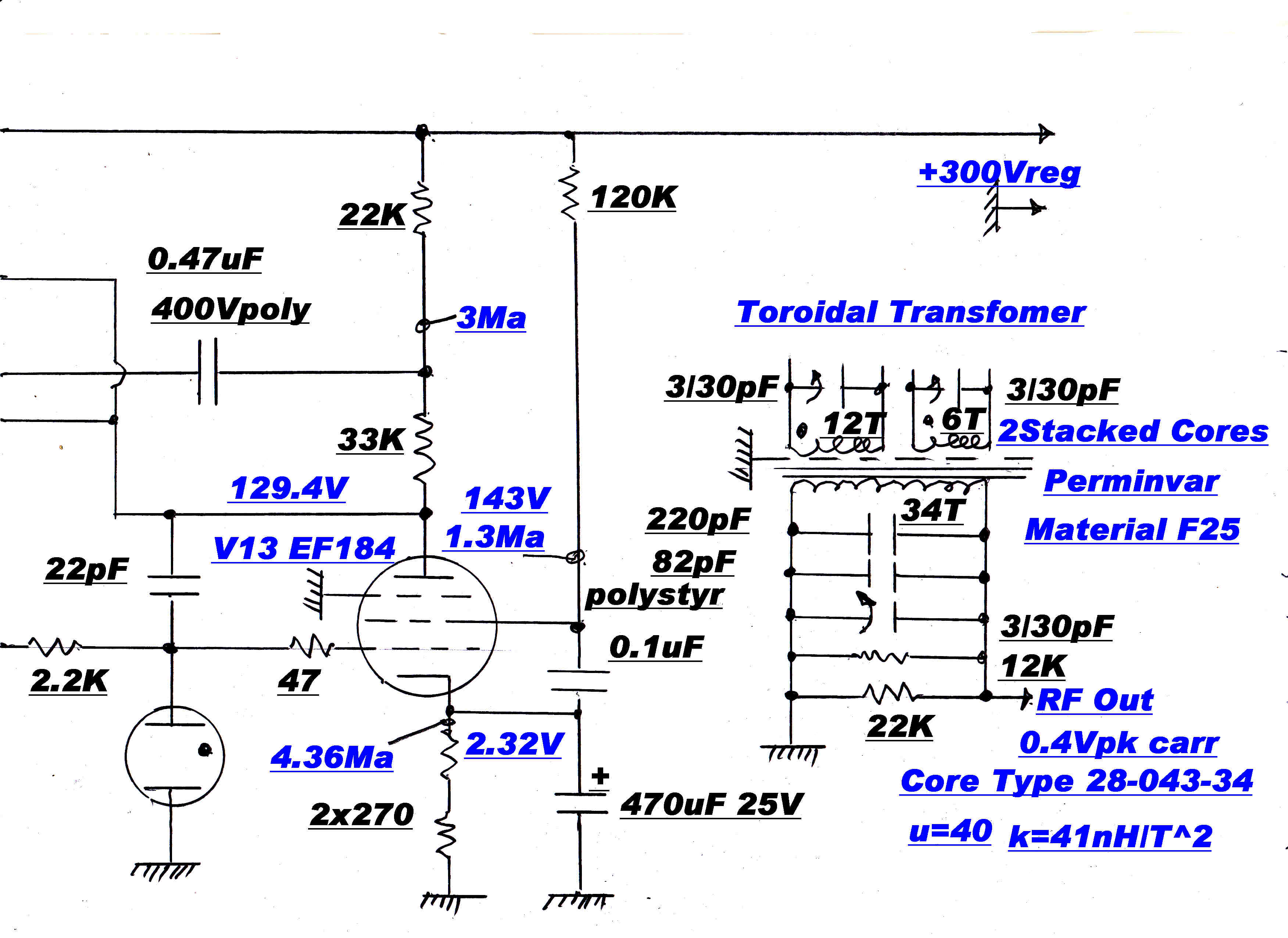
The full circuit of the L-C oscillator is shown above.
A beam deflection tube, V1, is used as the L-C oscillator. Isolation is provided by the
cathode follower V2a. The phase splitter, V2b, drives the full wave rectifier V3a, V3b.
The output of this is used as feedback to control the beam current, and hence the
oscillation level, in V1.
A beam deflection tube has the following attractive properties as an oscillator:-
[1] Positive feedback around the L-C tuned circuit is easily achieved because both
positive and negative Gms ( mutual conductances ) are available.
[2] When the deflection plate drive is sufficient to fully deflect the beam,
the plate current is a square wave. This greatly simplifies oscillator level control.
The transfer function, Ya(p), between the grid of the V1 and the RF drive to the full
wave rectifier is given by:-
Ya(p) = 1/( 1 + τap )
where τ = Q/( πfosc )
Here Q ≈ 80 : fosc = 739KHz. ; τa = 3.49x10⁻⁵
The response time of the full wave rectifier is smaller for increasing drive than
decreasing drive.The time constant, τb, for decreasing drive is
given approximately by:-
τb = (220pF)x(590k) = 1.3x10⁻⁴
Loop stabilisation can be obtained by making the beam tube grid time constant,
τc much greater than either of these.
τc ≈ (0.1uF)x(100k) = 10-2 Secs.
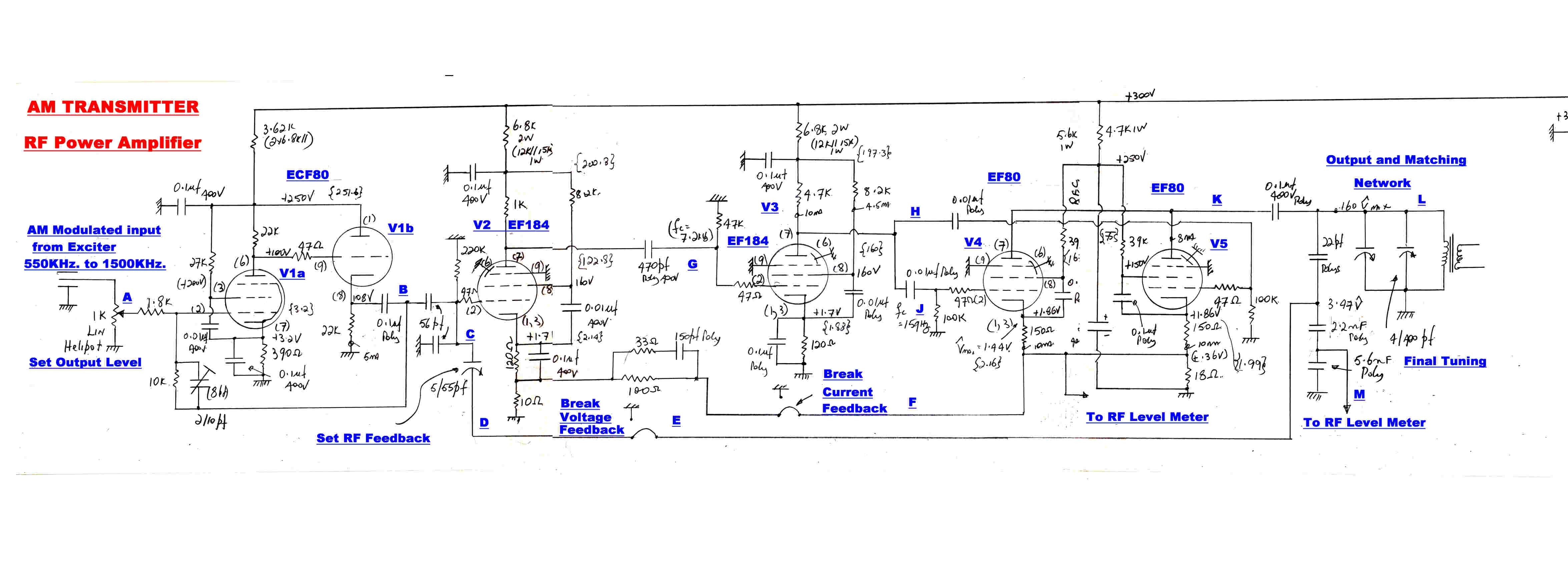
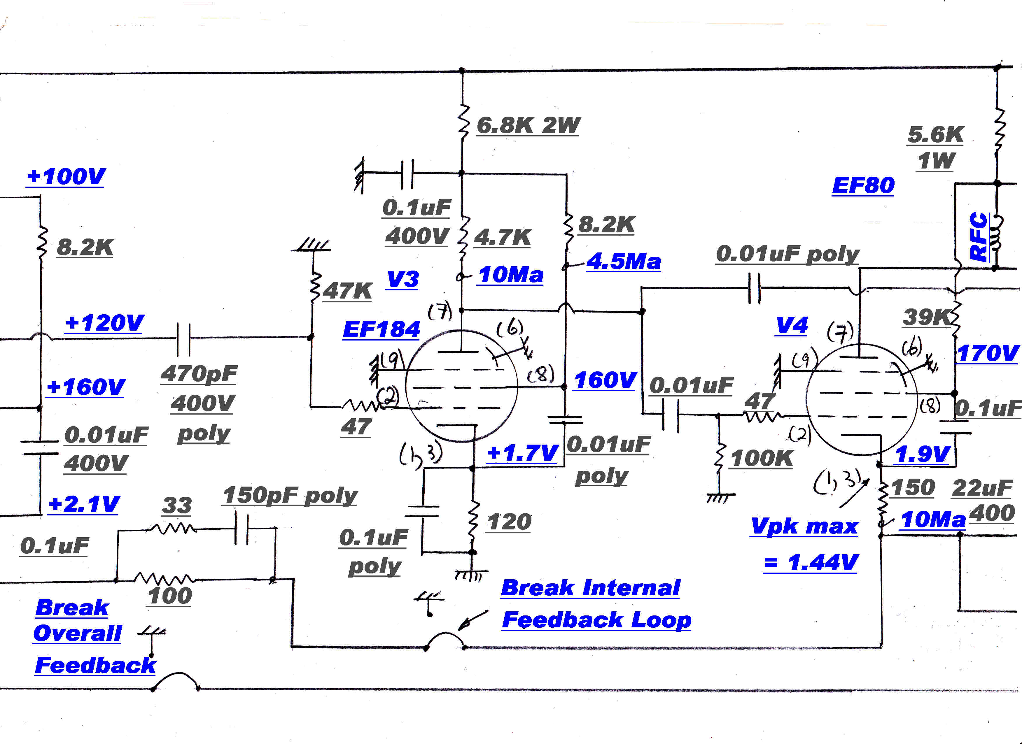
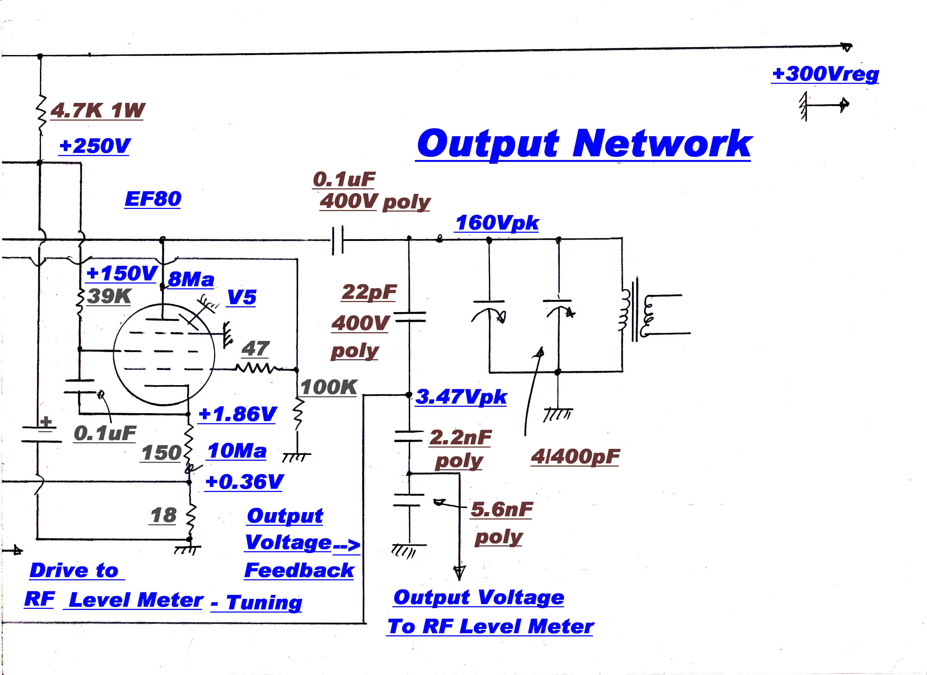
A Sketch of the Power Amplifier Circuit is shown above.
See below for an enlarged circuit.
The RF amplifier is broadband, so that the there is only one tuning control in the
output matching network.
The plate current in the output tubes V4, V5, is sensed in the 18 ohm common cathode resistor
and fed back into the cathode of V2 to give about 20db of current feedback.
This ensures that V2, V3, V4, V5, act as a constant current generator which is flat across
the broadcast band with minimal distortion.
The internal and suppressor grid shielding of the EF80 removes any interaction between the output
network and the current generator.
The output voltage on point L is divided down in a capacitive divider and fed back
to the grid of V2 to give heavy voltage feedback. This reduces the overall distortion still further
and ensures a wide bandwidth regardless of the loading of the matching network.
The R-C network in the plate of V2 produces a pole on the real axis at 10.6MHz. and
the R-C network in the plate of V3 produces a pole on the real axis at 2.26MHz.
The network in the feedback path produces a zero at about 10.6MHz. and a pole at about 30MHz.
This zero cancels the 10.6MHz. pole in the forward path to give two poles around the current loop
at 2.26MHz. and 30MHz..
With 20db feedback this provides good current feedback loop stability.
The correction network is placed in the feedback path rather than the forward path to give a shelf
which improves the voltage feedback loop stability.
The coupling network between V2 abd V3 ( 470pF/47K) has a 3db frequency of about 7.05KHz. This is more than 10 times higher than any other low frequency cutoff, so the forward path low frequency response falls at 6db per octave to well below the unity gain frequency giving good low frequency loop stability.
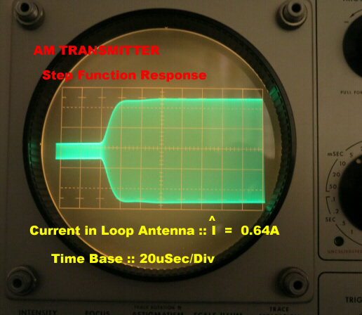
 The overall step function response is shown on the right.
Regardless of loading, the transmitter is flat to beyond 35 KHz..
At the time of the above tests the low frequency response had a 1.4db peak at about 10Hz. due
to the audio preamp in the modulator.
The overall step function response is shown on the right.
Regardless of loading, the transmitter is flat to beyond 35 KHz..
At the time of the above tests the low frequency response had a 1.4db peak at about 10Hz. due
to the audio preamp in the modulator.
This has been modified to give an overall response flat betwwen 10Hz. and 35KHz..
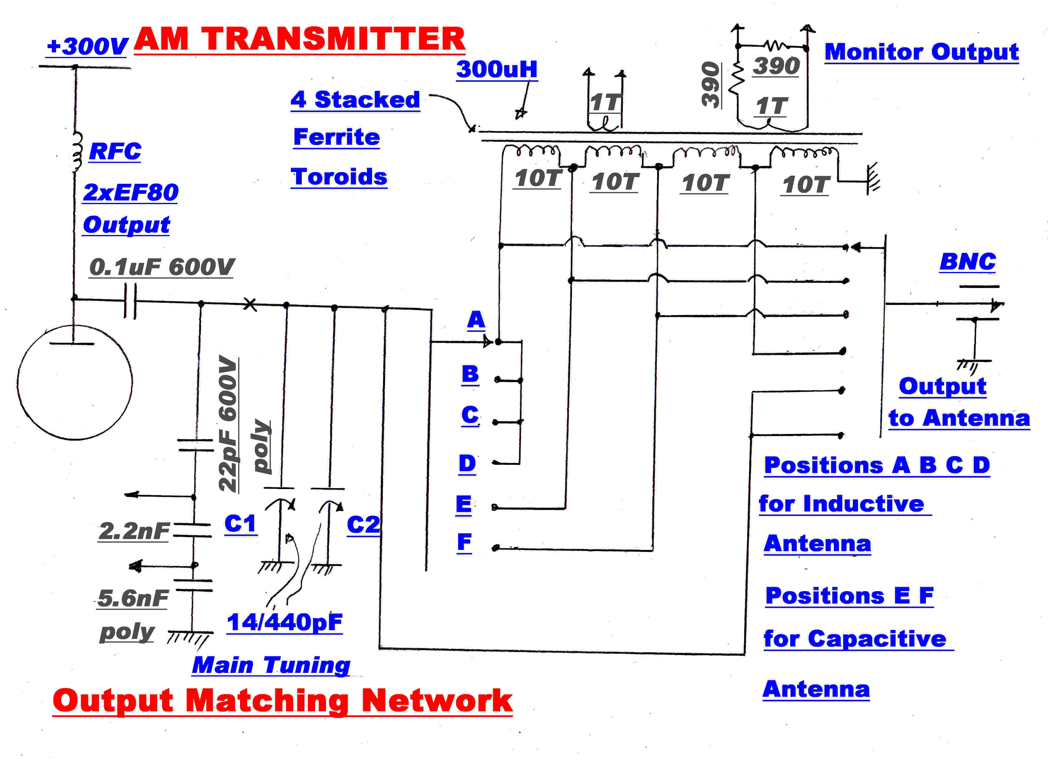 The RF matching network is essentially a parallel tuned circuit with taps.
Inductive and capacitive loads can be accommodated.
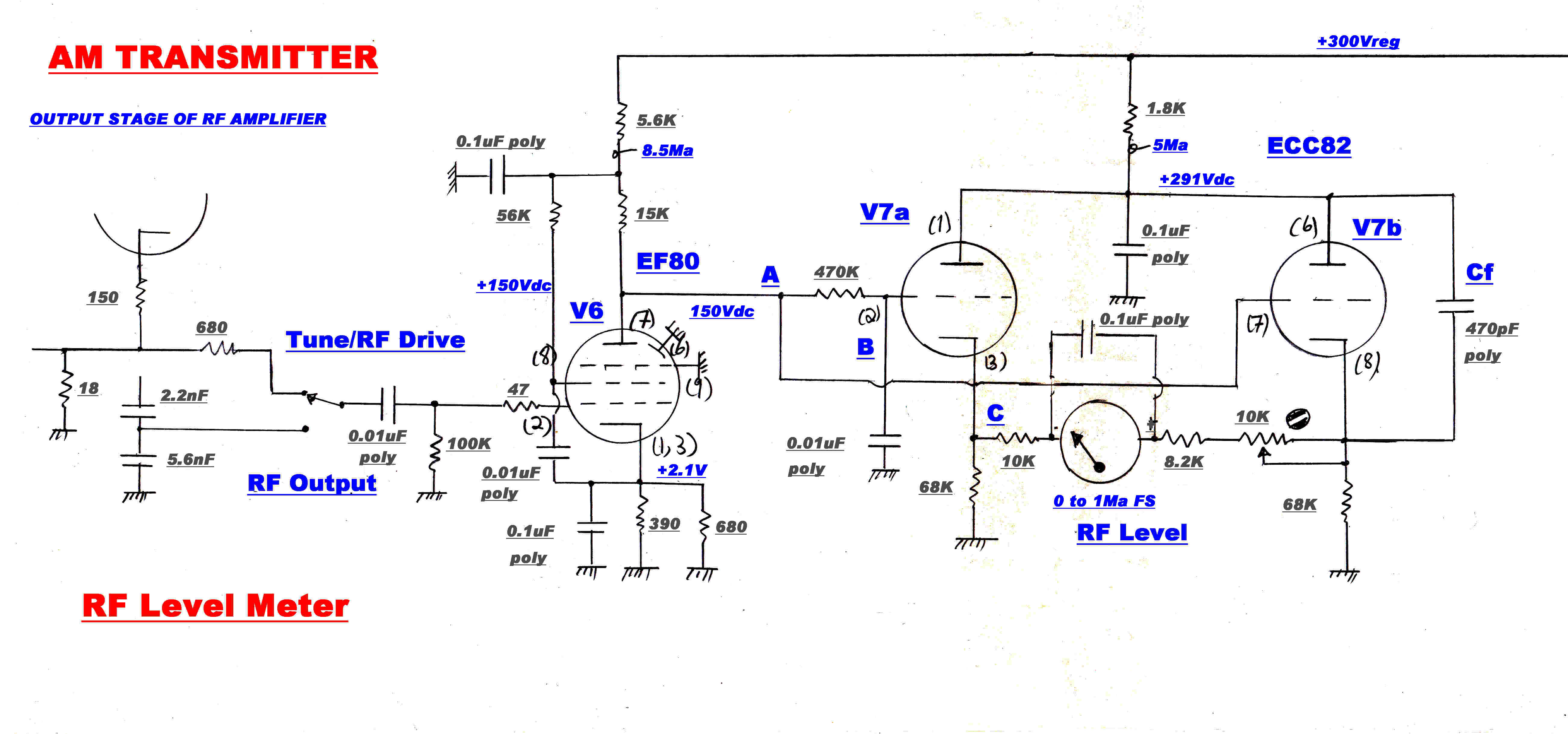
The circuit of the RF level meter used as a tuning indicator is shown above.
V6 is an RF amplifier. The DC on the plate is applied to the grid of V7a via the
470k/0.01uF low pass filter.
DC plus the RF is applied to the grid of V7b which acts as a peak rectifier because of the
capacitor Cf in its cathode. The cathode current is made large enough for the
rectifier to follow the modulation envelope, so linear detection occurs.
The potential difference between the the cathodes of V7b and V7a is then proportional
to the level of the carrier.
In the "tune" position, the level meter measures the RF voltage across the 18 ohm
common cathode resistor in the output stage. This gives an indication of the RF current drive
to the matching network. This is a parallel tuned circuit and presents the maximum impedance
to the output stage at resonance. The heavy voltage feedback ensures that the output voltage
remains constant as the circuit is tuned through resonance, and so the drive current has
a minimum at resonance.
THE MATCHING NETWORK IS TUNED FOR A MINIMUM
In the "run" position the output voltage across the tuned circuit is monitored
through a capacitive divider.
The output level can be set by the 1K helipot on the input to the RF anplifier.
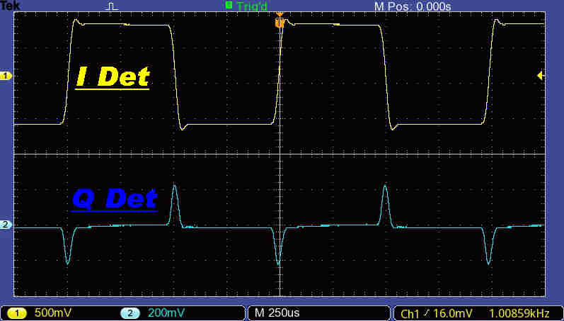
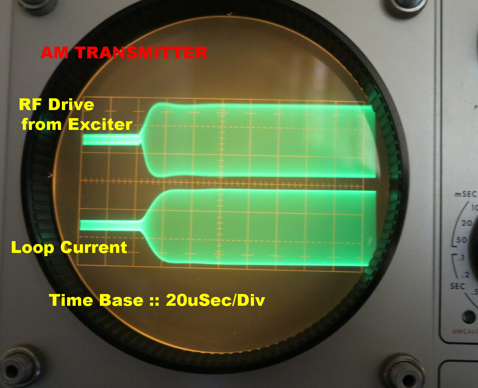
The overall 1KHz square wave response of the transmitter and tuner is shown on the right.
During the test, the tuner operated from its normal loop antenna.The transmitter drove a
small loop separated by about 20 metres.
The I or In-Phase product detector output was taken from the main audio output of the tuner.
The quadrature detector output was taken from the output on the front panel.
The small overshoot on both outputs is produced by third order maximally flat filtering
on the outputs of the product demodulators.
The output from the quadrature detector is of particular interest.
A small pulse appears during the square wave transition.
This is due to asymmetry of the amplitude and phase response at the outer limits of the pass band
as expected.
The remaider of the response is a straight line.
This implies :-
[A] The main part of the steady state frequency response of the transmittter and tuner is
symmetrical about carrier.
[B] There are no non-linear mechanisms to cause low frequency phase modulation.
|
|
|
|
|
|
|
|
|
|