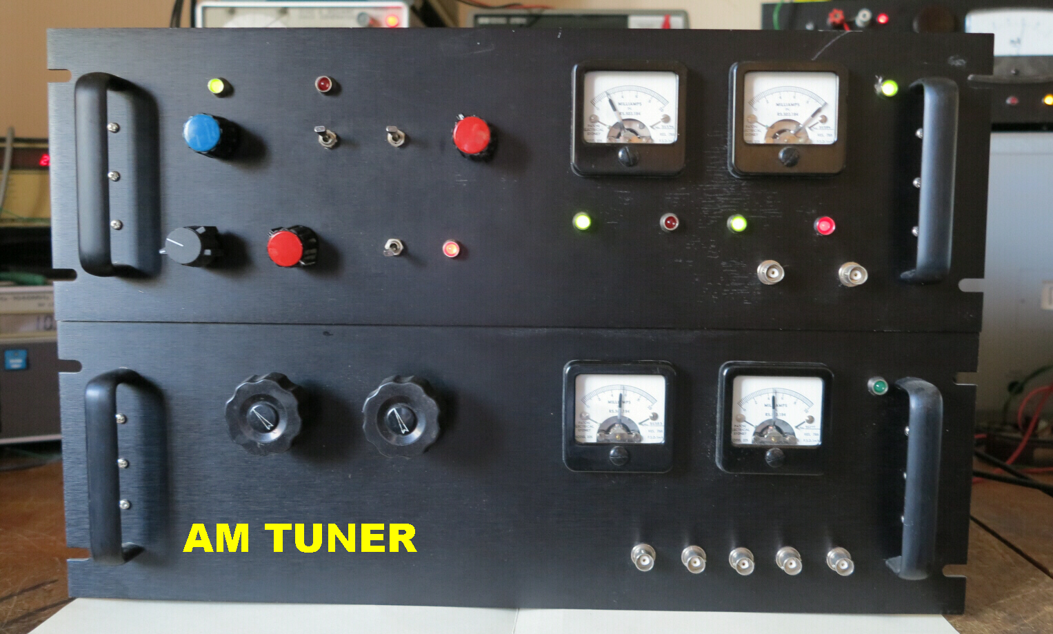
HIGH FIDELITY AM TUNER
CONTACT : COMMENTS AND QUESTIONS
back/home
This tuner was built for two reasons:-
(1) To demonstrate the excellent audio quality which can be achieved in a well designed AM transmisson system.
(2) As test gear to monitor the important parameters of the local AM broadcast transmitters.
Great attention is paid to reducing distortion to an insignificant level. A large amount of feedback is applied
to all RF, IF and audio stages.
AGC
----------
Distortion introduced by Automatic Gain Control " AGC" presents two serious problems in the design of AM tuners.
[1] The non-linear elements used to control gain introduce distortion.
Here the gain is controlled by variable resistors in resistive dividers. The variable resistors are temperature sensitive in indirectly heated
thermistors.
These introduce no distortion, but their thermal lag causes stability problems in the tight AGC loop.
Stability is restored by a fast loop operating in parallel with the thermistor loop. This controls the level of local oscillator injection
into the mixer - so changing the conversion transconductance.
THIS LOOP IS ACTIVE ONLY DURING CHANGES OF SIGNAL LEVEL TO THE TUNER.
[2] The AGC must be very slow so that it does not mistake low frequency modulation for a change in level and attempt to suppress it.
This is a non-linear process and causes distortion.
The tuner has two AGC time constants -
SLOW for run
FAST for tuning
TUNING ACCURACY
------------------------------
To minimise quadrature modulation the carrier must be centered exactly in the passband of the tuner.
This is achieved with xtal accuracy.
The carrier on the output of the 455KHz IF strip is phase locked to a 455KHz crystal oscillator by controlling the frequency
of the local oscillator. The pull in range is about +(-) 30KHz.
The Xtal oscillator output can now be used as the reference for in-phase and quadrature product demodulators.
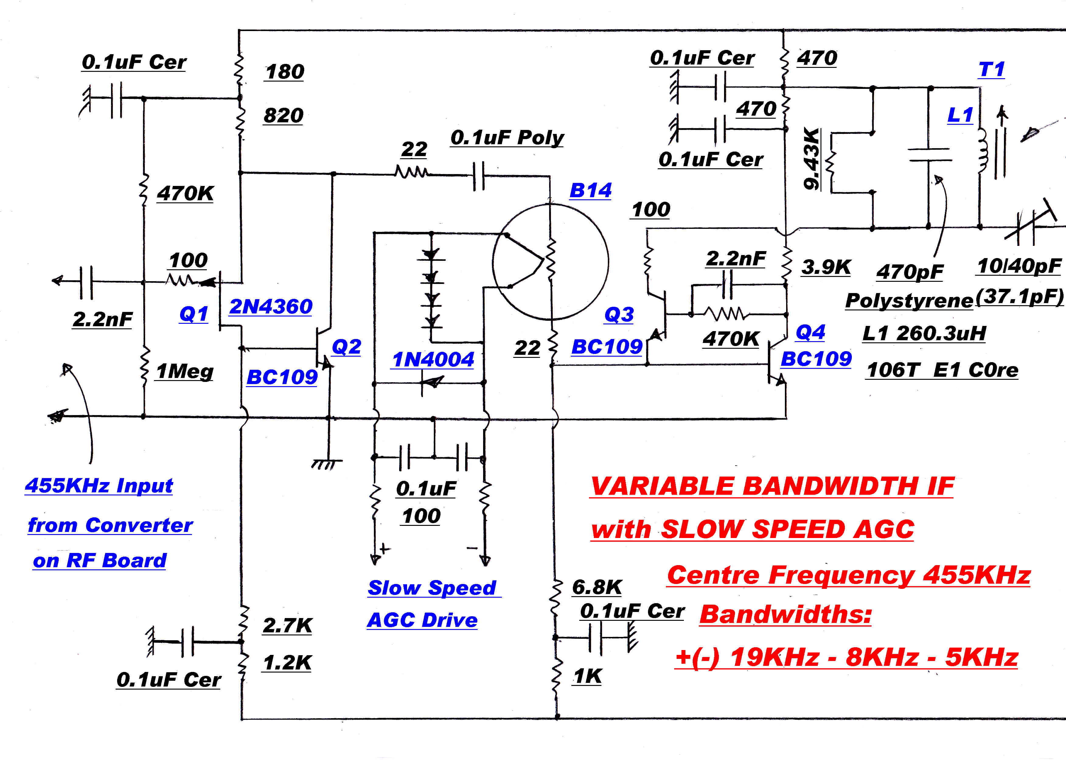
BANDWIDTH
---------------------
The maximum total bandwidth of the tuner is 36KHz, giving an equivalent modulation bandwidth of 18KHz.
The transfer function in the wide band position is seventh order - three poles on the real axis to give a gaussian
response, together with two second order networks to give a maximally flat response.
This provides an overall transient response with little overshoot and a response which is nearly phase linear
and symmetrical about the carrier up to 10KHz, so that insignificant carrier phase modulation is
introduced by the tuner.
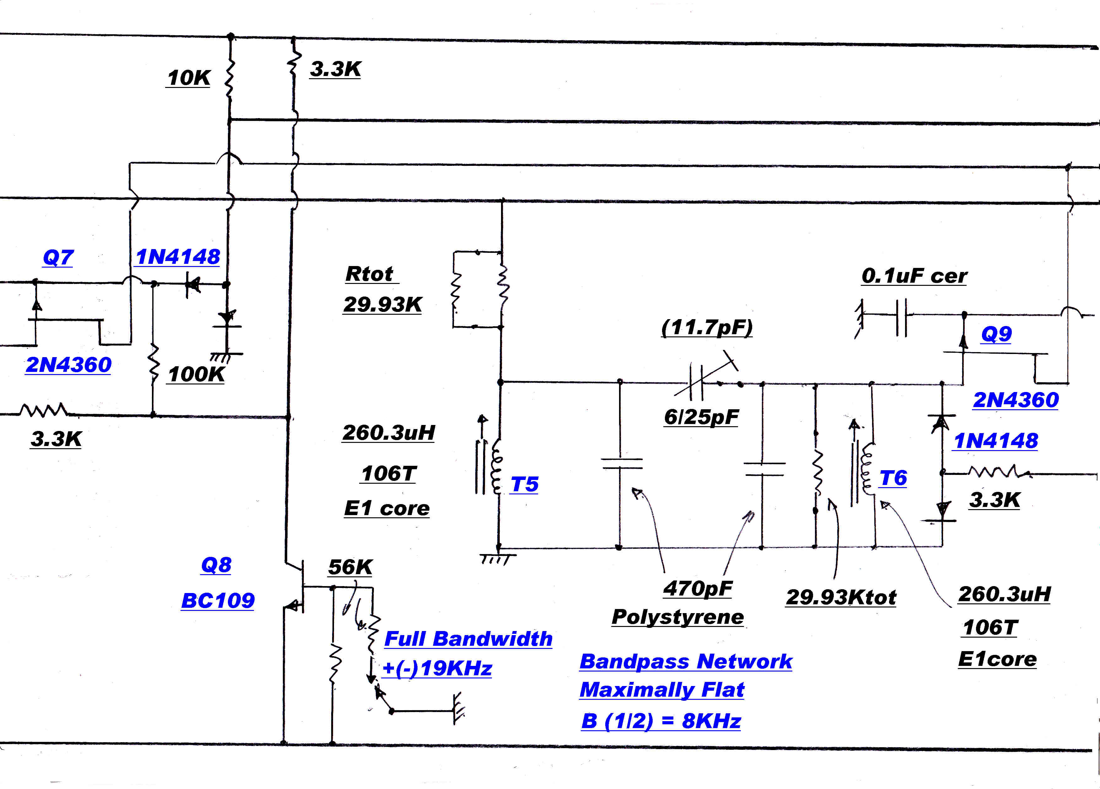
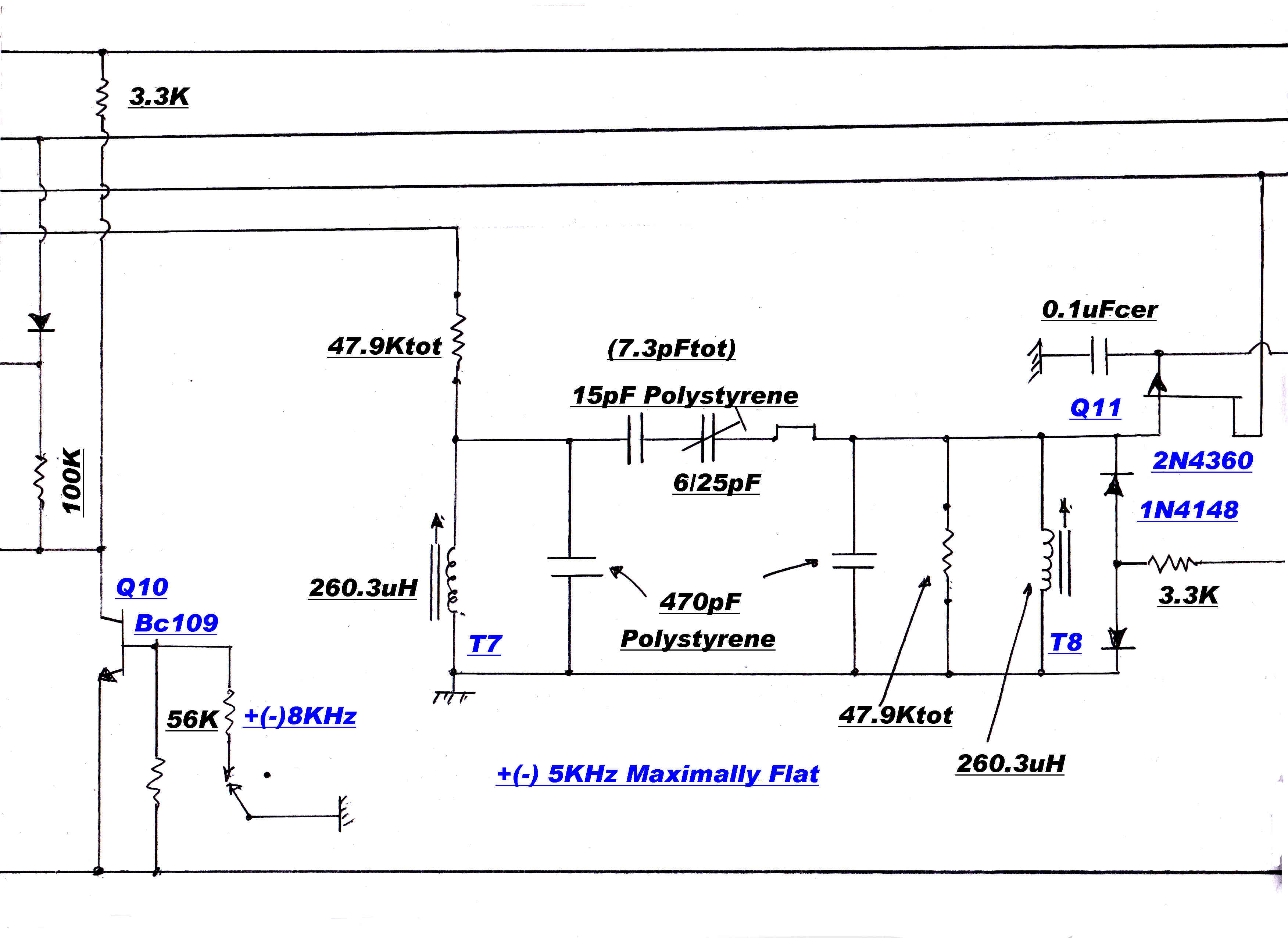
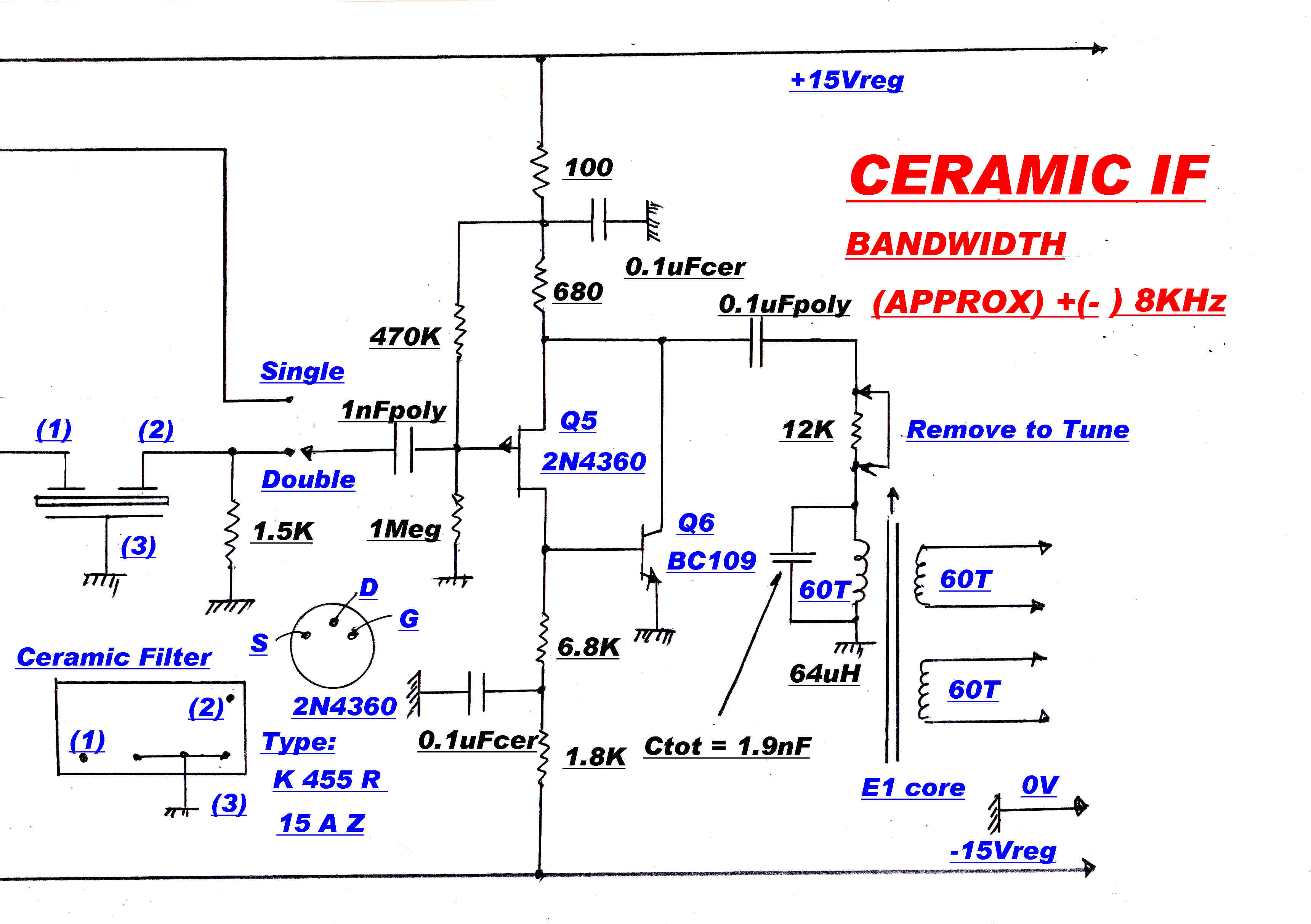
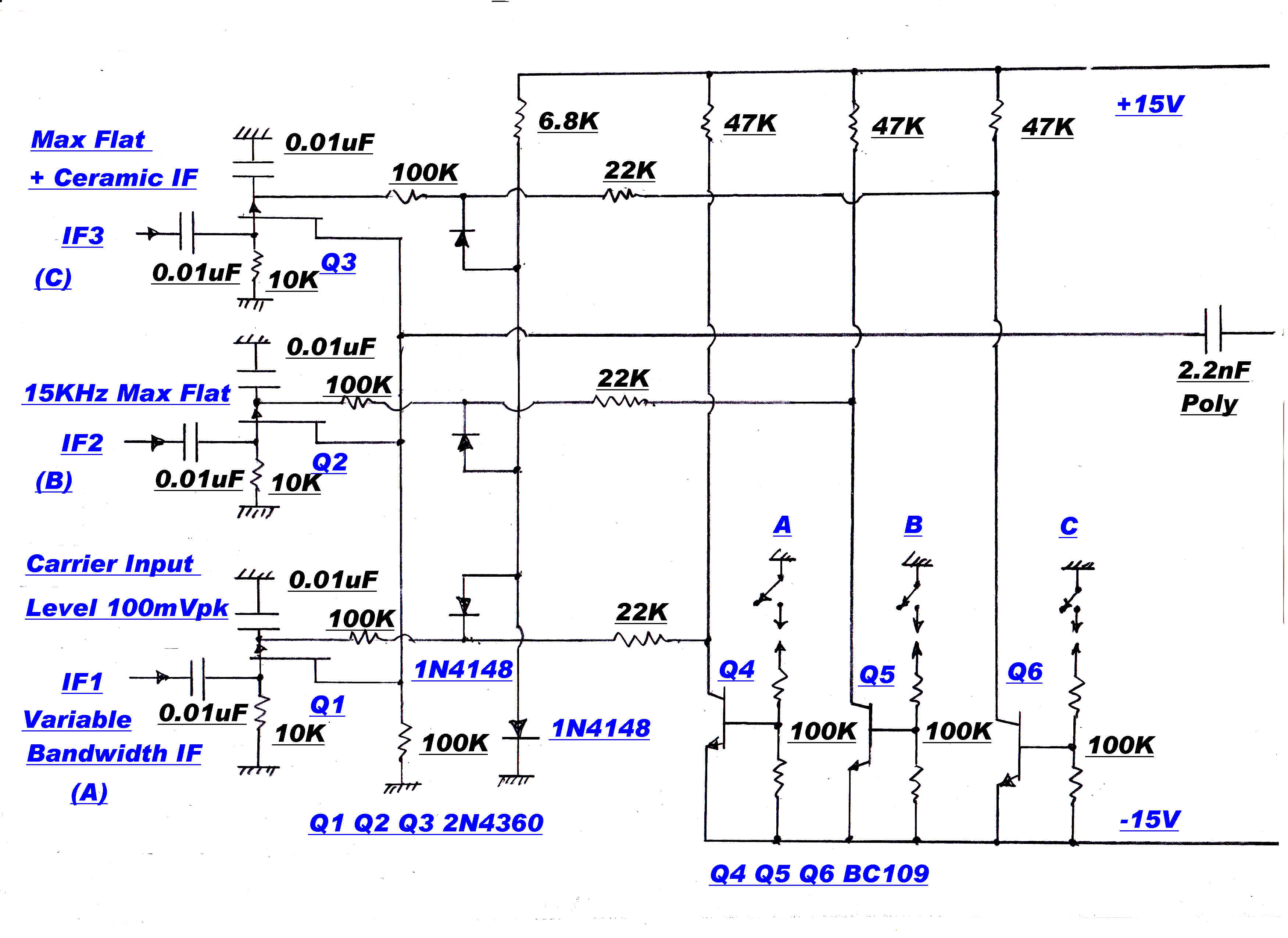
Second order maximally flat 8KHz and 5KHz filters may be added to the IF when appropriate.
A fifth order 30KHz maximally flat filter and a double 16KHz Xtal filter with extremely sharp skirts
may also be added.
Although the tuner is intended for high quality reception, a variable depth 9KHz audio notch filter
and a peak audio limiter have been included. These are switchable and normally not used.
The outputs from the tuner are as follows:-
ANALOG METERS
(1) Input carrier frequency - 500KHz to 1500KHz.
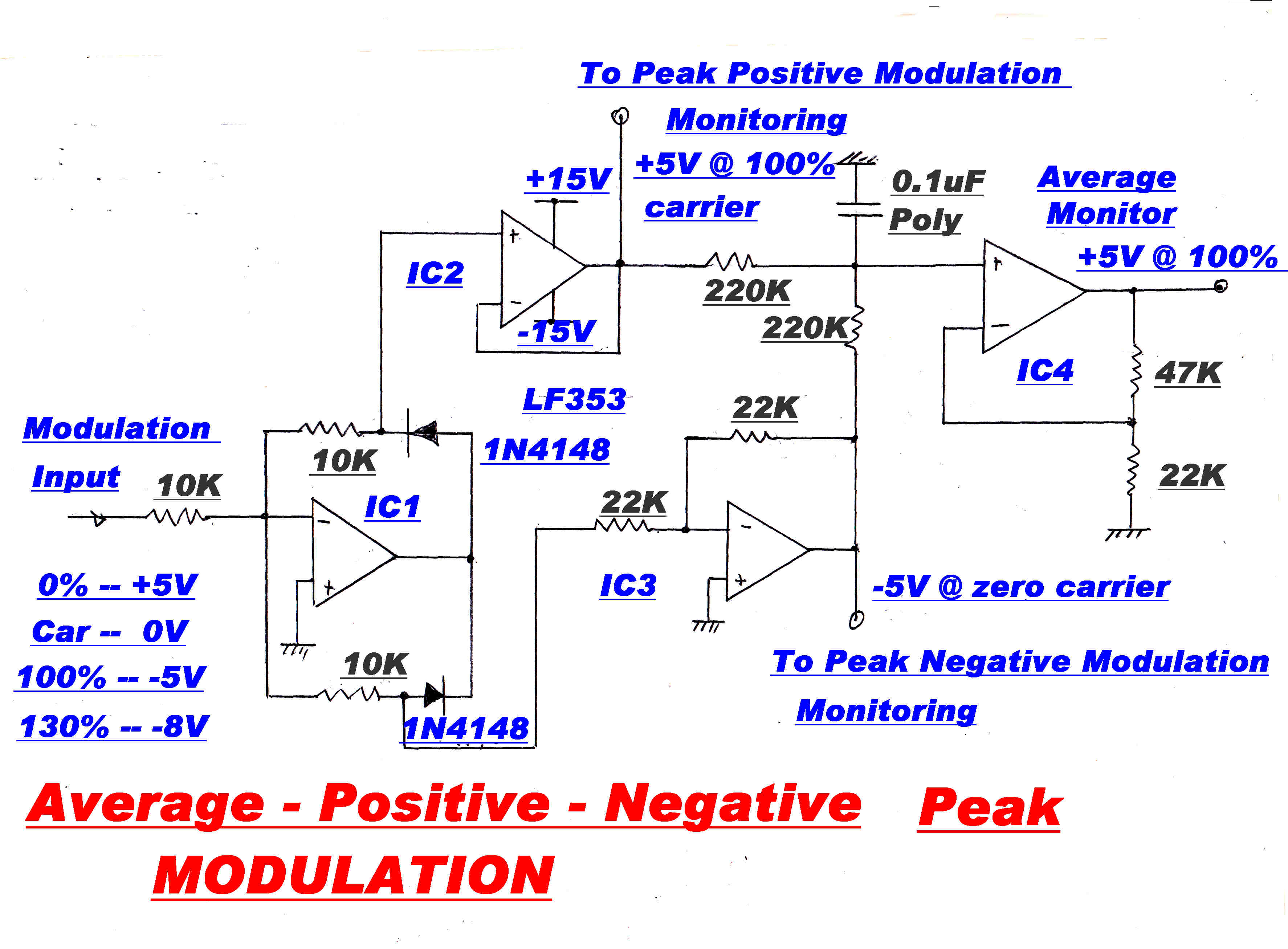
(2) Modulation level - Average 0 to 100% : Negative peak and hold - 0 to 100% : Positive peak and hold - 0 to 125%
(3) Tune Mode: Tuning Frequency Error.
Run Mode: Phaselock Loop Error. Normally Zero : Only departs from zero under fault conditions.
(4) S meter with a logarithmic response.
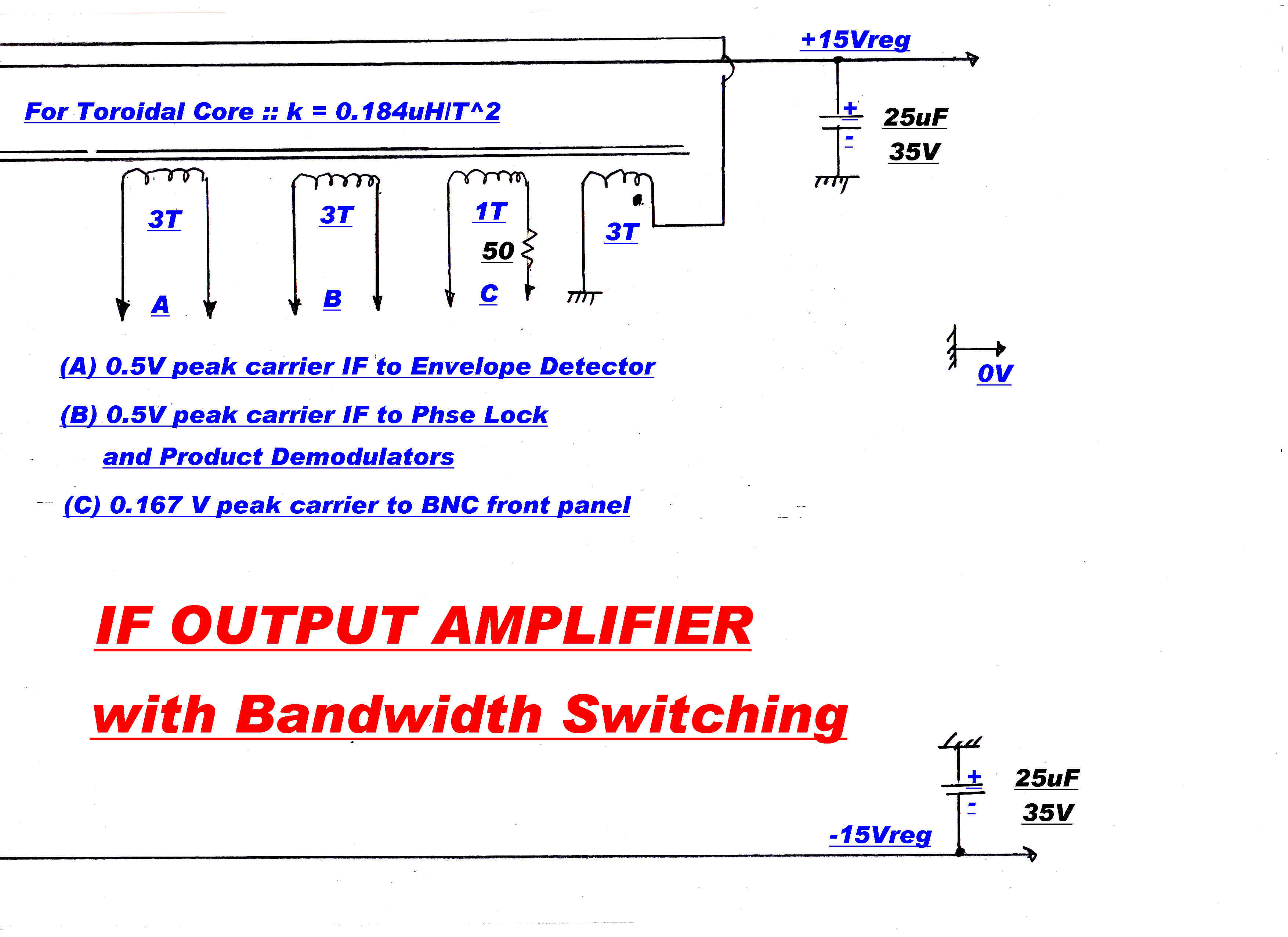
SIGNAL OUTPUTS ON BNC CONNECTORS
(1) 455KHz IF -- Carrier level 0.167 V
(2) Envelope Detector Out
(3) In - Phase Product Detector Output
(4) Quadrature Product Detector Output
(5) Phase Modulation on Carrier -- 5.7 degrees/volt
(6) Reconstituted carrier stripped of modulation for carrier frequency measurements.
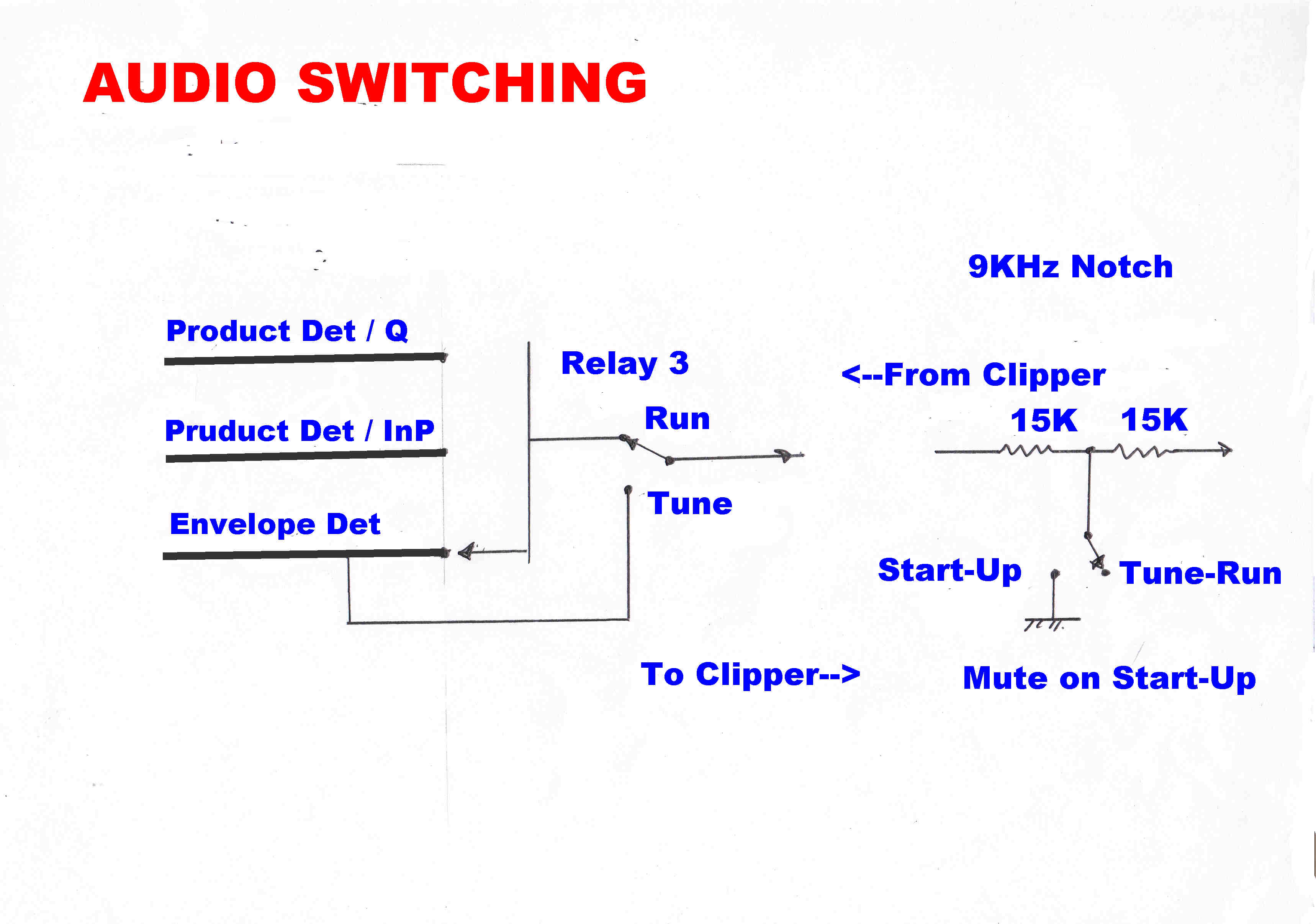
(7) Audio Output: Automatically switched to Envelop Detector during Tune. May connect to Product Demodulators when
PLL error is zero.
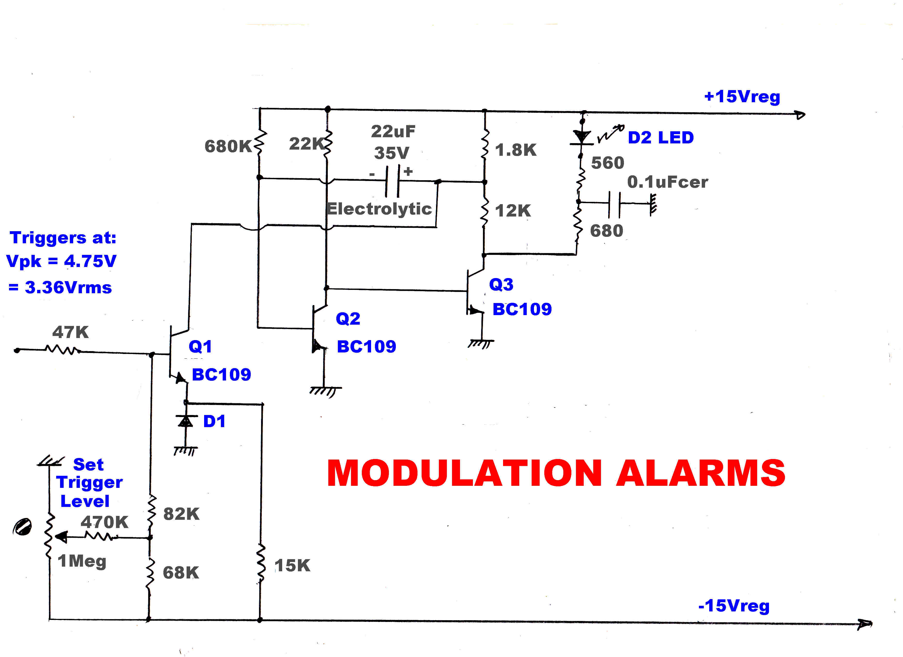
ALARMS
(1) RED:Modulation Greater than 97%
(2) GREEN:Modulation Below 3%
Note:With the audio processing used at the present time at the transmitters these are "ON" almost continously.
General Discussion of Design Problems
Some salient design features and problems encountered in the design are mentioned here.
They are discussed in more detail in the appropriate section.
AGC and its Problems
AGC Response Time
A meter indicates the average, the positive peak and the negative peak modulation. The calibration can be correct
only when the IF carrier output is constant and independent of the signal input level.
This implies infinite DC gain - or the use of an integrator - in the AGC loop.
The dynamics of the AGC loop are also important.
A fast AGC loop will attack the amplitude modulation, regarding it as a change in signal level. This is a non-linear process
and low frequency distortion will result.
A slow speed AGC loop will not correct the large variation in signal strength in tuning from station to station resulting
in loud bursts of distorted audio.
The only solution is to have fast AGC during tuning and slow AGC during normal operation. This is possible since ground
wave transmission is very stable.
The slow AGC time constant is chosen to give no visible distortion to an input modulated 100% with a 10Hz sinusoid.
AGC Gain Control Element - Distortion
The mechanism to achieve the variable gain to give AGC should produce no distortion.
A variable resistor is the ideal control element. This is realised in an indirectly heated thermistor.
The dynamics of the indirectly heated thermistor present great difficulties in an AGC control loop :-
(A) It is slow - response time 3 to 4 seconds.
(B) Because of the thermal delay it has a non phase-minimum transfer function, and this leads to instabilities under feedback.
In spite of the difficult dynamics, the thermistor was chosen, since the reduction of distortion was of primary concern.
AGC Dynamics - Loop Stability and Response Time
The dynamic problems were solved by splitting the gain control function into two parallel paths - one with a very fast
gain control mechanism and the other with the slow thermistor control.
Note: The control transfer function of gain controlled stages in series ADD, and so appear to be in parallel. See below.
The primary AGC loop integrator drives both paths in parallel. The thermistor path includes another integrator.
This ensures that the steady state error in the fast loop is eventually forced to zero, returning the gain in the fast
loop to a target value.
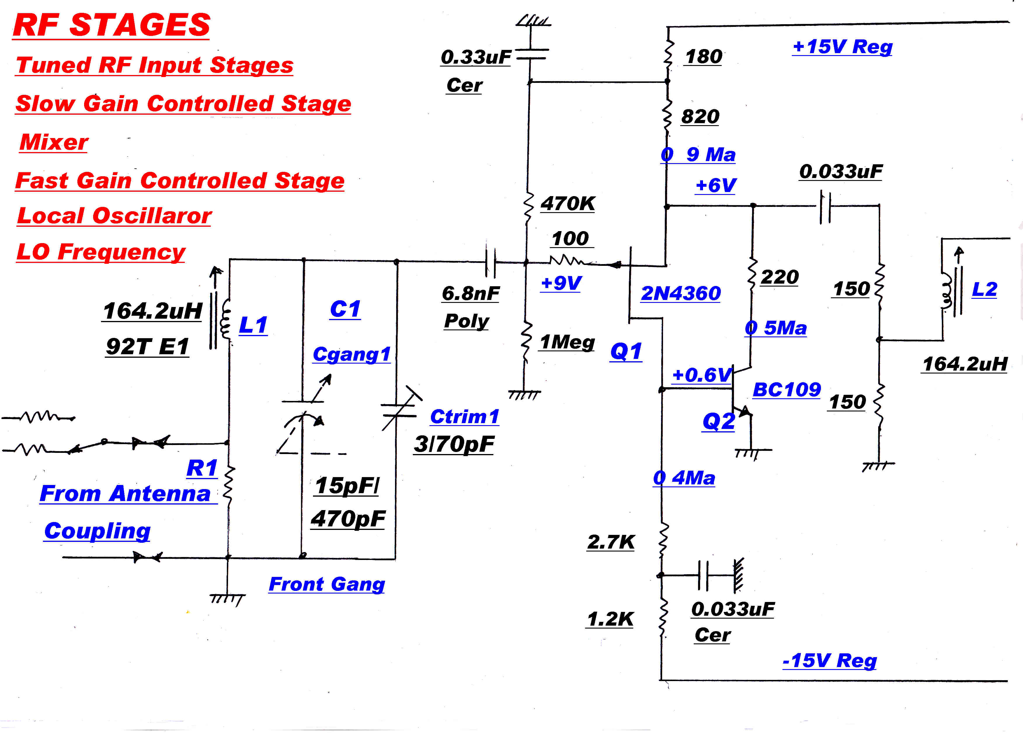
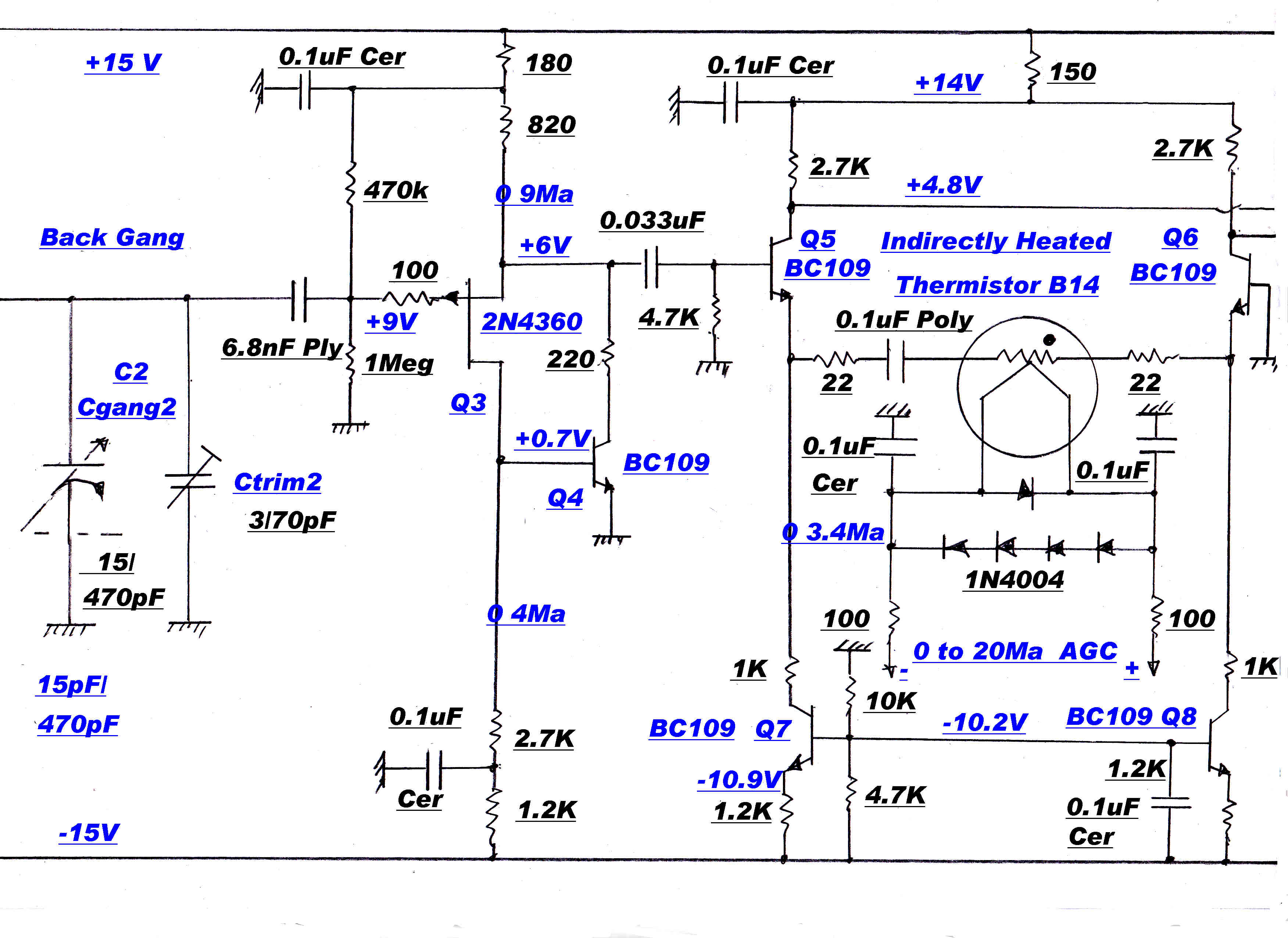
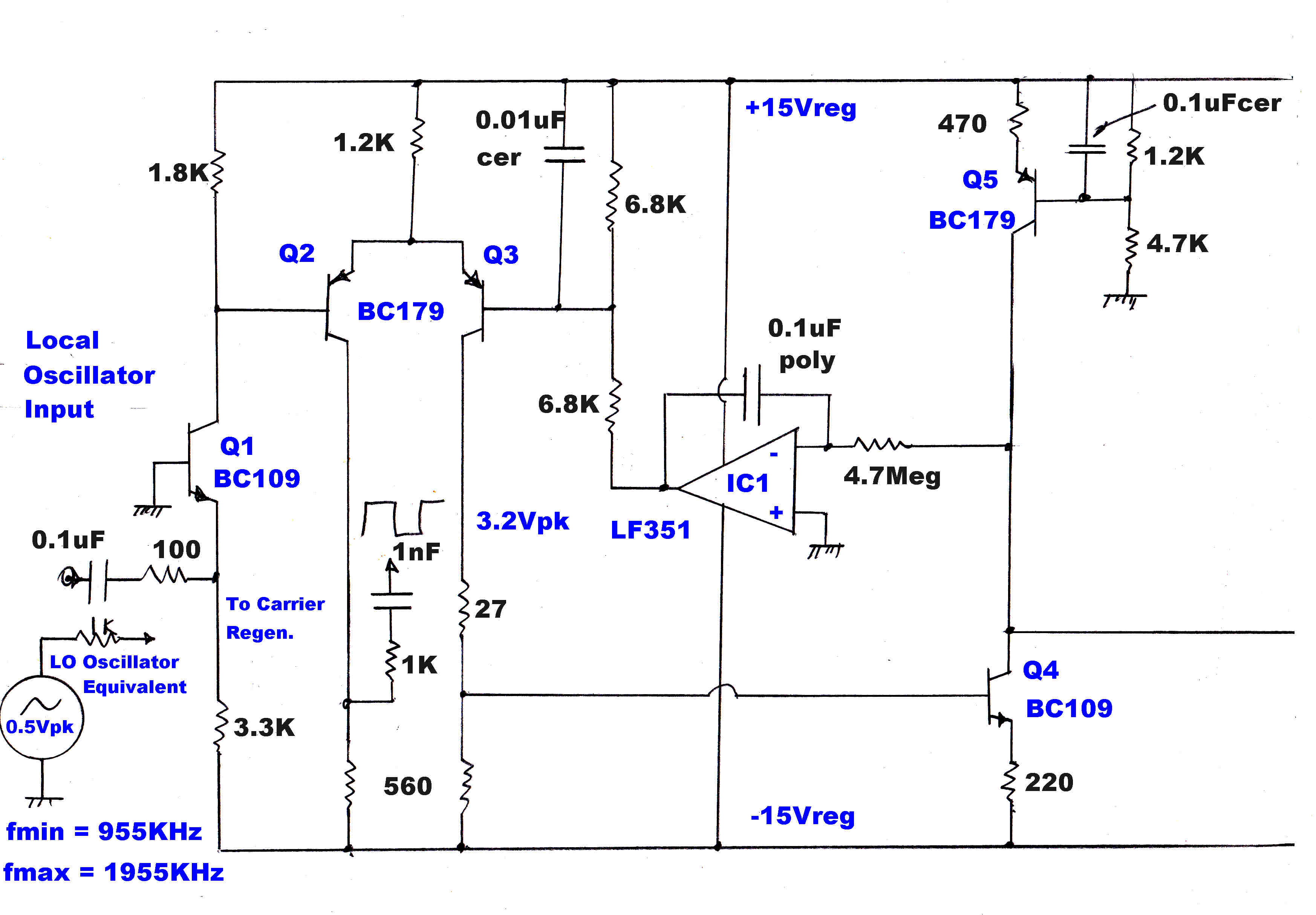
Fast loop gain control ocurs in the RF-IF frequency converter. This is operated in the non-saturated mode, so the
conversion transconductance varies with the local oscillator injection level.
The AGC voltage varies the injection level - the transconductance - and so the gain.
The scheme can only be successful if the conversion process introduces negligible distortion to the modulation content.
The mixer topology resolves into a long tail pair with a current drive into the common emitters. It is shown below that
no distortion occurs if the transfer characteristic of the active elements (BFY90) in the long tail pair is exponential.
A quiescent collector current of 1.14 MA for each transistor gives an excellent approximation, and hence virtually
no distortion, at the operating signal levels.
The mixer is the only RF - IF stage NOT under heavy feedback.
The critical frequency in the AGC loop occurs when the gain of the fast loop equals the gain of the slow loop.
Above this frequency, the dynamics of the AGC loop is equivalent to an integrator with negative feedback.
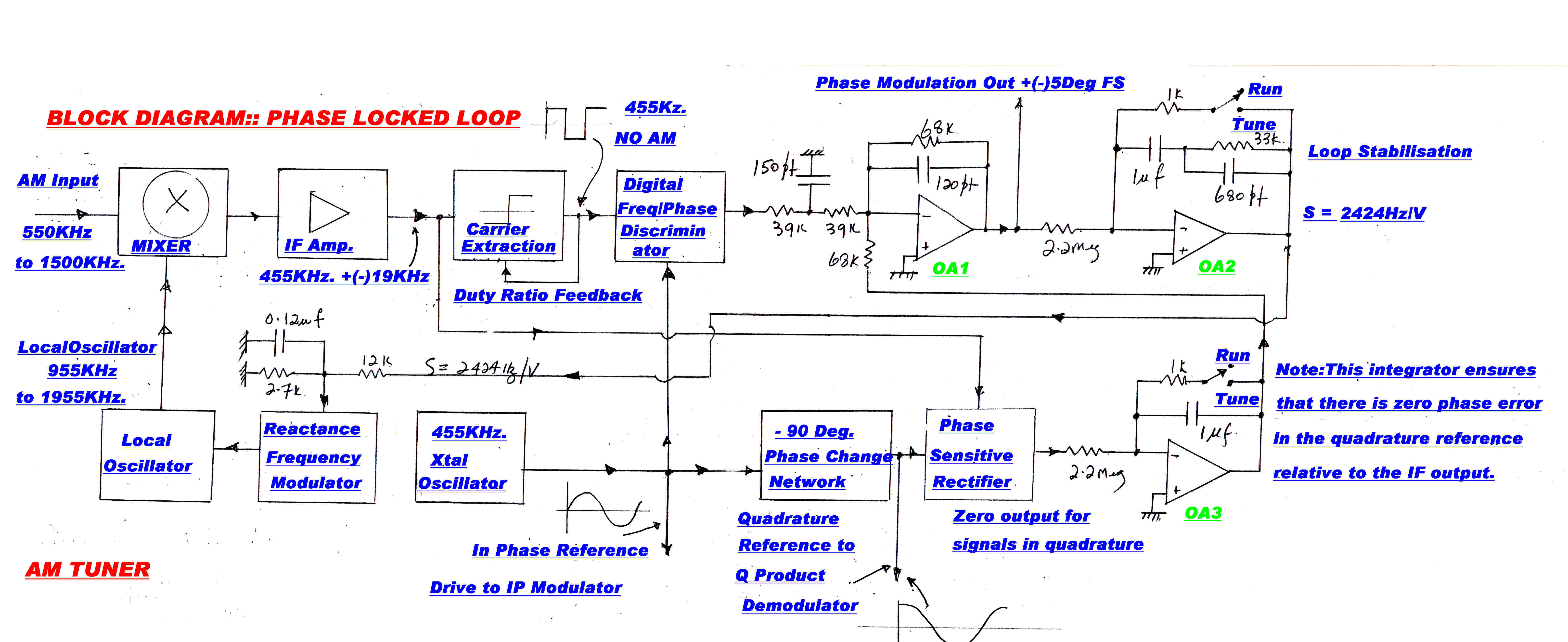
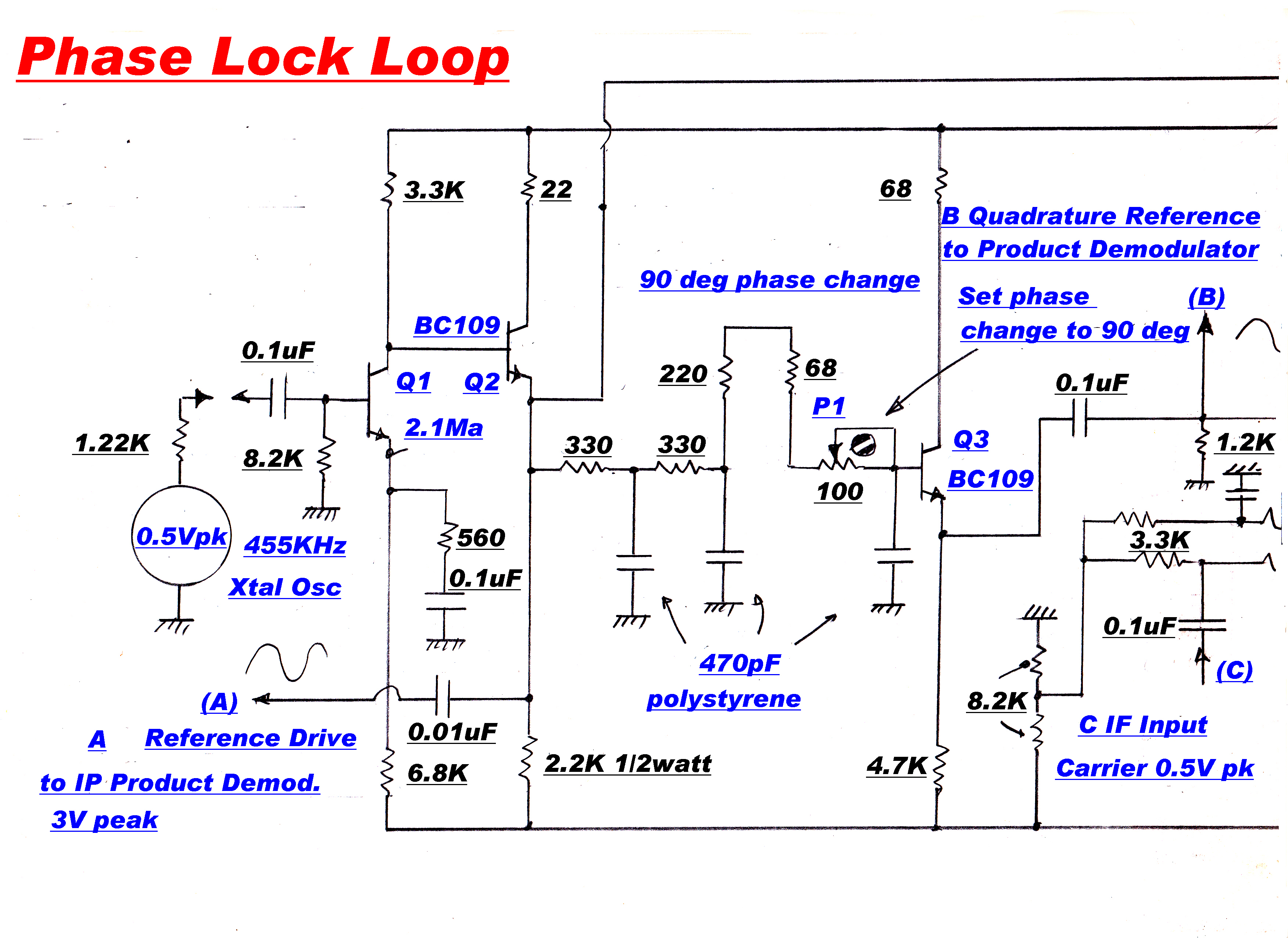
The Phase Locked Loop
Topology
The in-phase and quadrature product demodulators and the carrier phase dectector require a restored
carrier stripped of all amplitude and phase modulation.
This is usually generated by a phase locked loop in which a local oscillator is locked to the output of the IF.
The phase locked loop in this tuner operates in an entirely different way.
The IF frequency is locked to a 455KHz Xtal oscillator by controlling the frequency of the local oscillator.
This ensures that the IF frequency is always centred in the IF pass-band with Xtal accuracy.
Two other features result from this topology:-
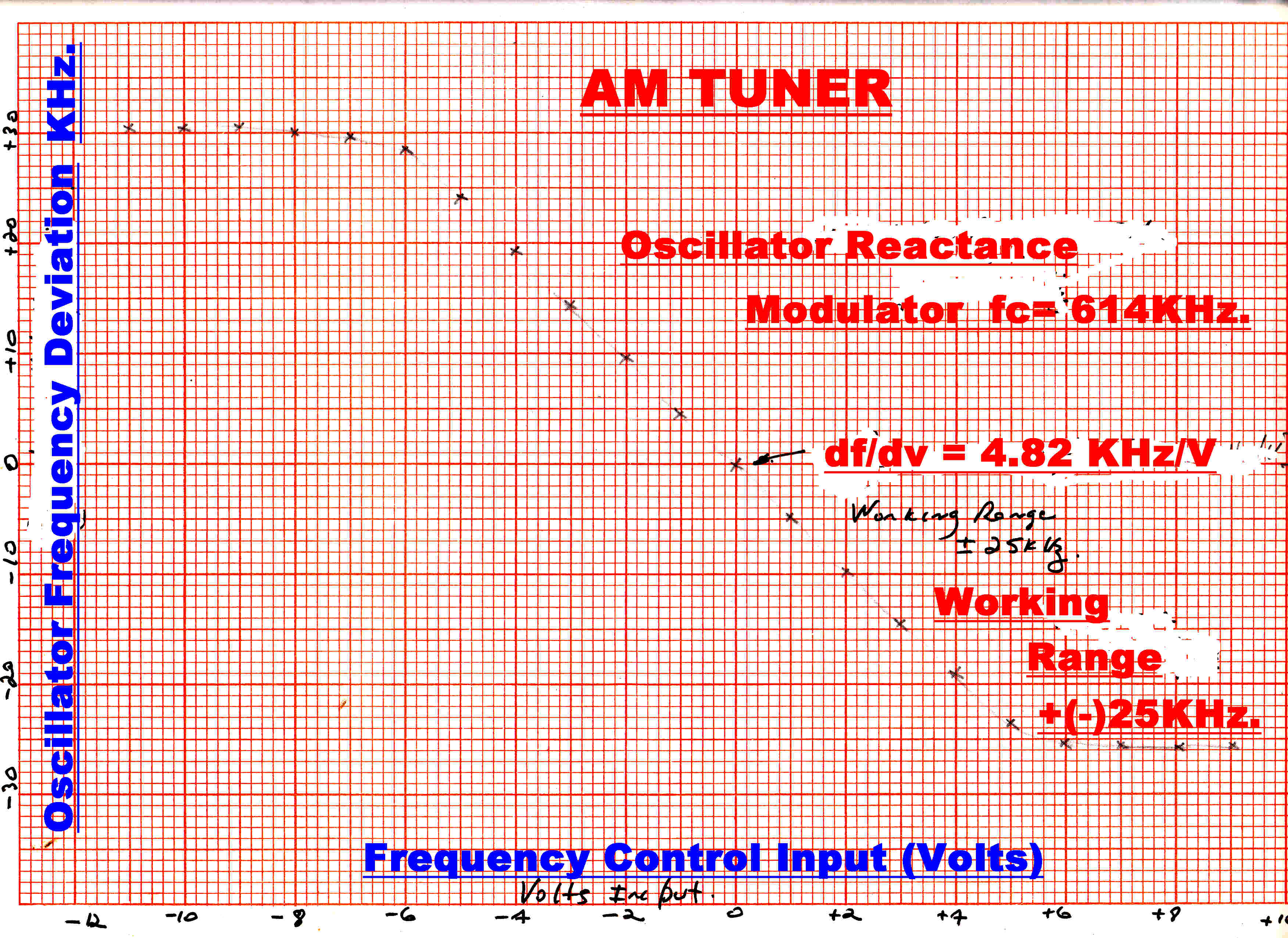
(1) The pull-in range of the local oscillator is +(-)28KHz, so the position of the tuning
capacitor shaft is not a unique function of tuning frequency. The local oscillator frequency is.
The local oscillator frequency is converted in a linear frequency to voltage converter, and the result
presented on the front panel on an analog meter calibrated 500KHz to 1.5MHz.
This gives a tuning indicator calibrated in KHz.
(2)The tuning of the input RF amplifiers is determined uniquely by the position of
the three gang tuning capacitor, and so may not be centered about carrier.
This is not acceptable, since it will give false results for the quadrature and phase modulation measurements.
The procedure to centre the RF stages is simple:
[A] With the receiver in the "RUN" mode make a small perturbation to the tuning knob.
The phase locked loop is fully active, so no change occurs to th IF frequency.
The AGC loop is in the "SLOW" mode and will not make an immediate correction if there is a change
in signal amplitude due to a change in tuning of the RF stages.
Since there is no correction, the S meter will flick in the direction of change and then resettle
as the AGC loop regains control. This gives a sensitive indication for the direction in which to correct the tuning.
The tuning is centered when a small perturbation of the tuning knob makes no change in the S meter.
Any tracking error is also removed.
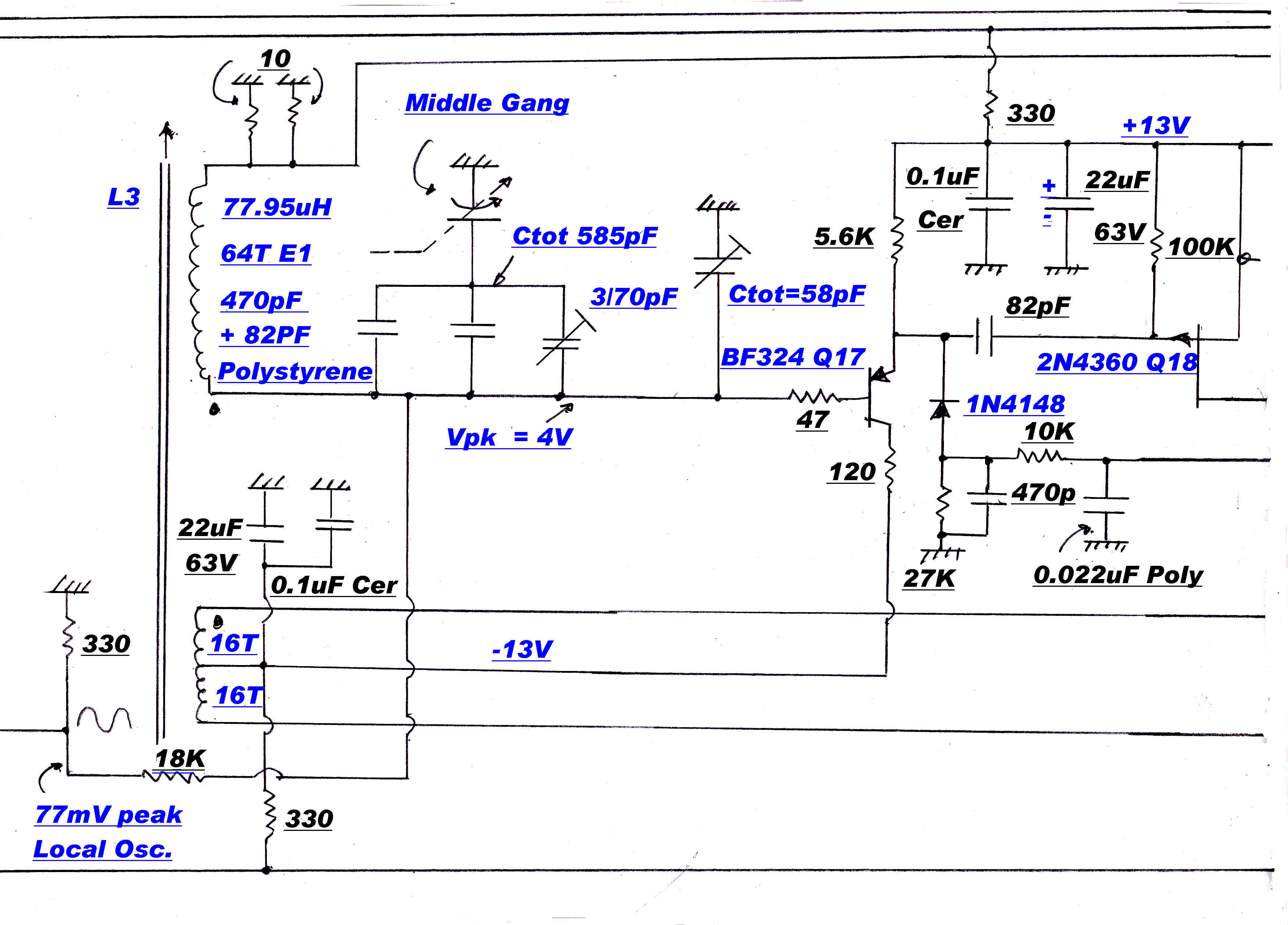
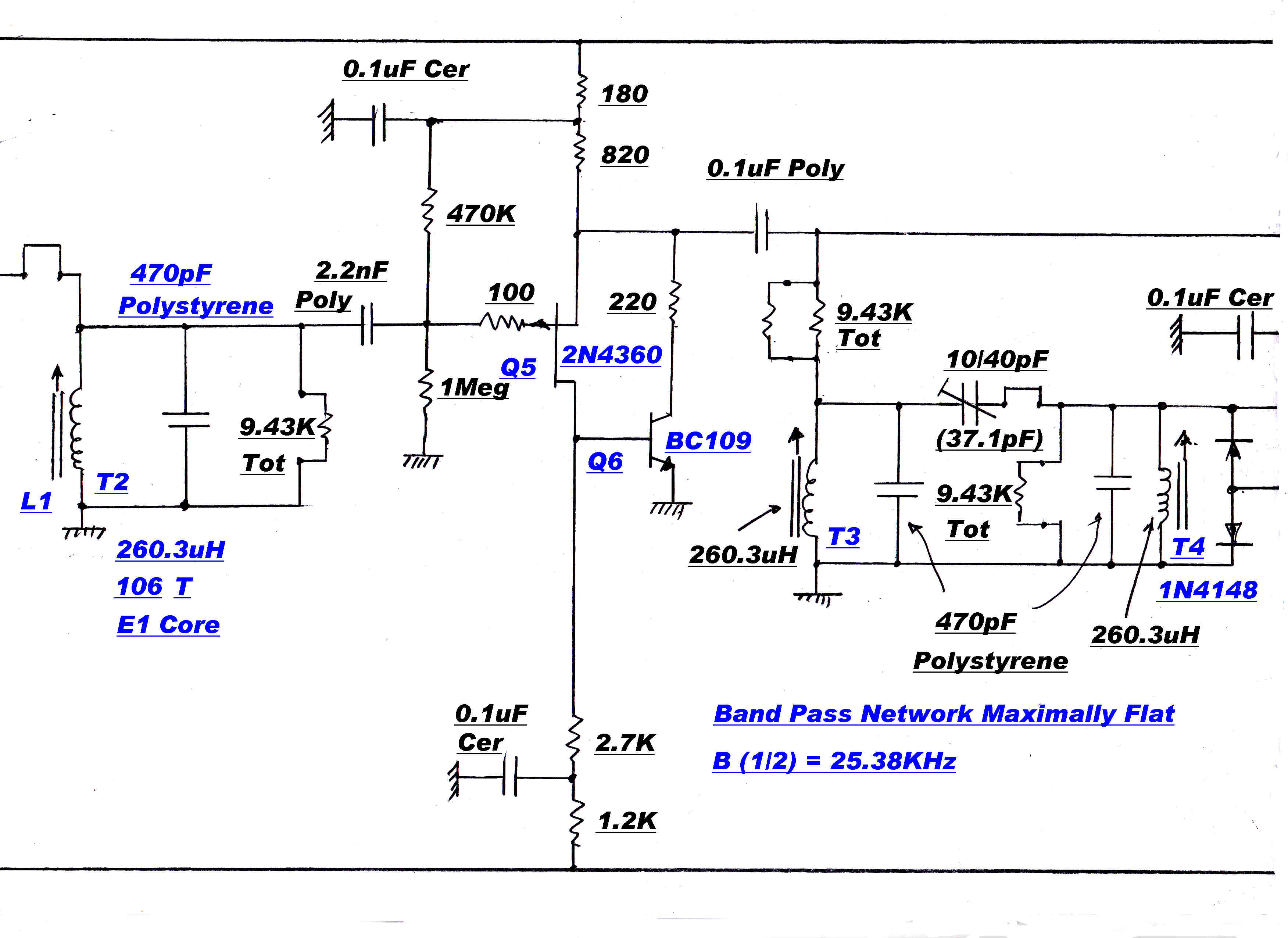
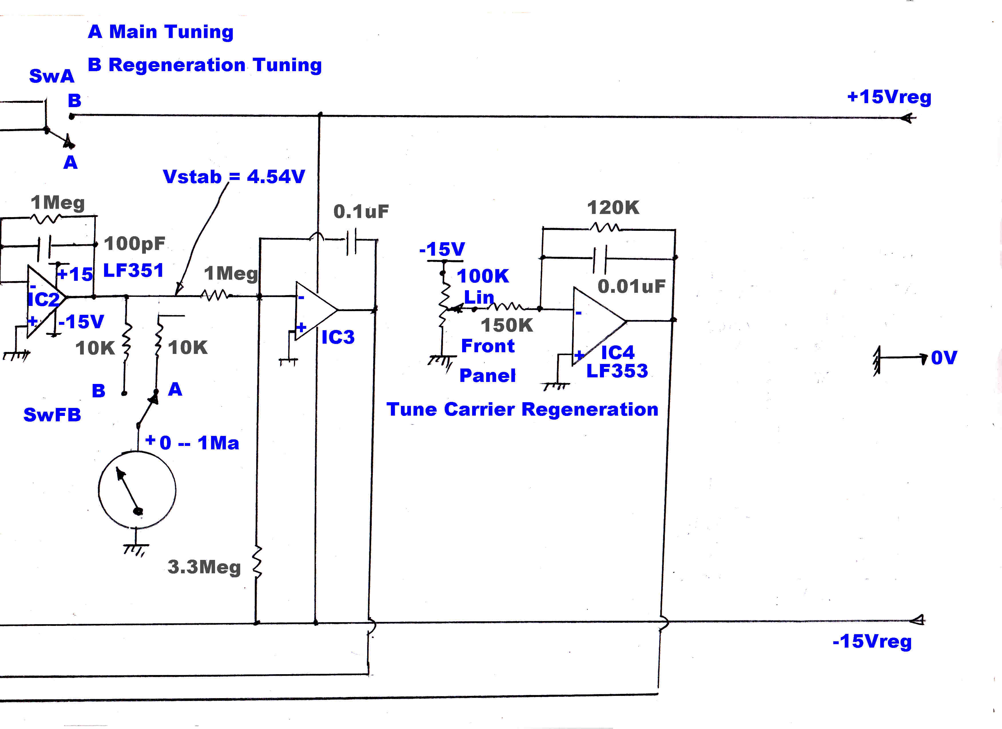
Tuned RF Networks
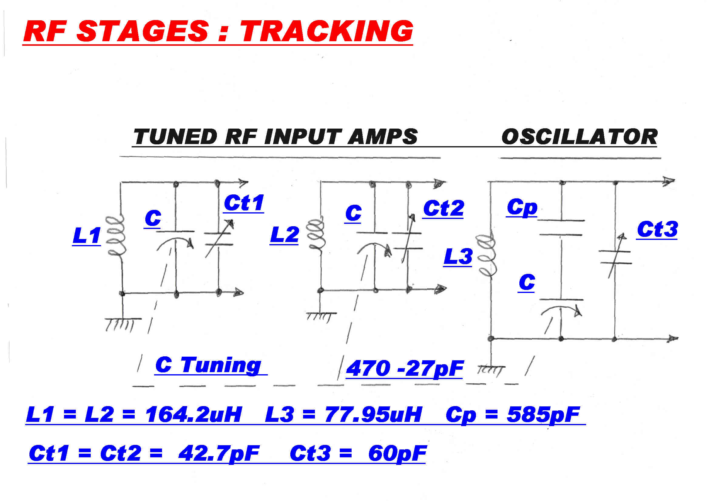 The RF networks involved in tuning are shown opposite.
In the "TUNE" position the voltage controlled reactance across the oscillator L-C is disabled and the tuning frequency is
uniquely determined by the variable capacity C.
The tuner then behaves as a normal superhet with tracking error.
Note: The oscillator trimmer capacitor Ct3 is not in its normal position directly across the tuning capacitor.
It is in parallel with the oscillator tuning inductor.
In this position it can directly absorb the stray capacity of the inductor. It also reduces the complexity of the analysis.
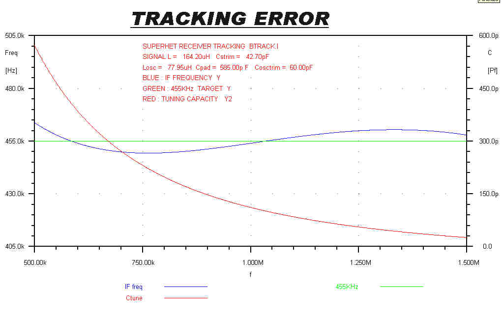 A plot of the IF frequency versus tuning frequency in the "TUNE" position is shown opposite.
The IF frequency error is about +(-) 5KHz.
This is removed by the tuning process described above.
The half bandwidth of both RF tuned circuits is 36.8KHz, so small tuning errors make very little
difference to the overall transfer function.
Phase Loop Errors
In the phase locked loop, the amplitude modulated carrier is sliced to remove the AM. The slicer employs heavy
duty ratio feedback to ensure that there are no phase errors or changes in amplitude in its output
when the carrier falls to 1% or below.
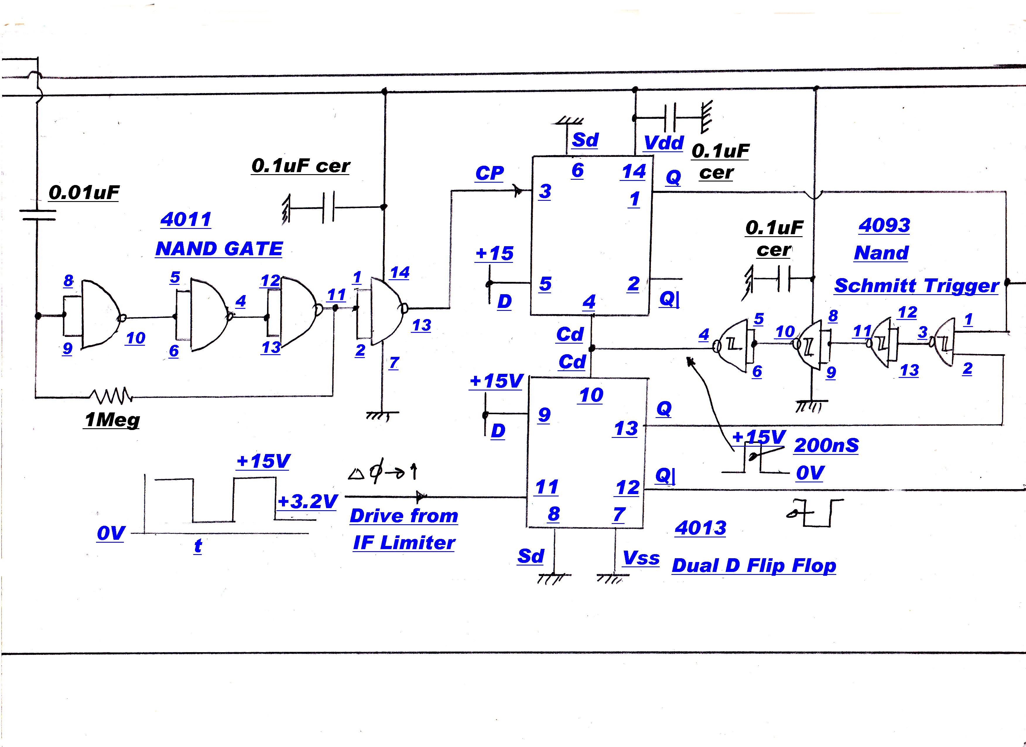
A frequency discriminator ensures initial pull-in and a phase discriminator ensures phase lock. The phase discriminator
determines the phase error in the loop, since a loop intgegrator forces the phase discriminator output to zero.
The phase and frequency disriminators employ digital circuitry.
The quadrature carrier is derived from the in-phase reference by a third order R-C phase change network. This is possible since
the carrier frequency is always 455KHz with Xtal accuracy.
This topology used in the initial design proved inadequate and was changed to the system described below.
It is vital that the departure of the quadrature carrier from 90 degrees be very small.
The in-phase demodulator responds according to a cos law, so that a 3 degree error will result in a response
down by cos(3) = 0.9986.
The quadrature detector exhibits a sin law, so that a 3 degree error will give an in-phase component
in the output of 0.0523.
This will mask any small quadrature component.
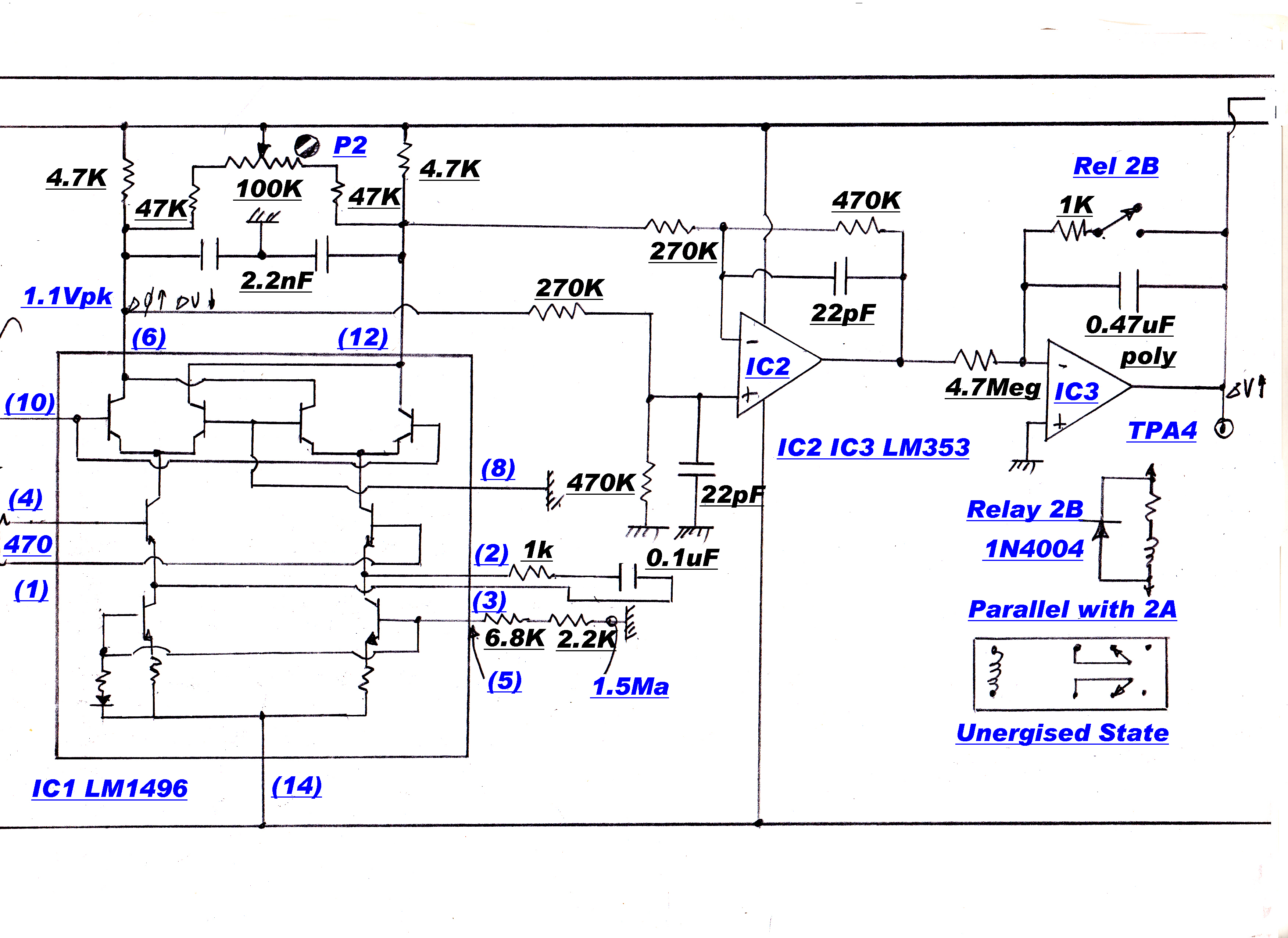
Phase Loop Error Correction
The addition of a phase sensitive rectifier driving a slow speed integrator stabilises and reduces
the quadrature phase error to acceptable limits.
The modulated IF and the quadrature reference are applied to a phase sensitive rectifier. The output drives
a very slow speed integrator. Its output is then added algebraically to the output of the digital
phase discriminator.
The integrator will eventually dominate the loop with the condition that its input is zero.
This means that the output from the phase sensitive rectifier is zero; and this occurs when the inputs are in quadrature.
Any errors or drift will appear in the in-phase reference, but as shown above, this is of little consequence.
Carrier Phase Modulation
The frequency of unity gain in the phase locked loop is about 70 Hz, so that all phase variations on
the IF below this frequency are attenuated on the output of the phase discriminator. Since the discriminator is linear,
its output represents the phase modulation on the carrier above 70Hz.
The mid-frequency phase modulation is usually due to non-linear effects in the transmitter.
For example a PI matching nework driving the grid of the final in a vacuum tube transmitter.
Variation of grid current over the modulation cycle in the final produces a variable load and so phase change.
Phase modulation at the upper end of the audio spectrum is usually due to asymmetry in the response of the matching
network and radiators.
Multiple element directional antennas usually present more problems than single omni-directional monopoles.
The calibration of the modulation meters and alarms demands that the carrier
level on the output of the IF strip be independent of the RF input signal level.
This implies that the DC gain around the AGC loop approach infinity.
The speed of the loop is also very important. If the AGC loop is active at the lowest
modulation frequency, it will treat this as a change of signal level
and attempt to reduce its amplitude.
This process is non-linear and produces distortion.
An integrator included in the AGC loop fulfills both conditions:-
(a) Its DC gain approaches infinity.
(b) Its time constant can be increased until the loop is no longer active
at the lowest modulation frequency to be received.
This tuner will handle a 10Hz 100% modulated input with no distortion.
The propagation of ground wave for the local AM service is very stable, so that
slow speed AGC responses are adequate.
On the other hand, relatively fast responses are required during tuning.
The tuner therefore has two modes:-
(1) The RUN MODE with slow AGC.
(2) The TUNE mode with fast AGC.
It is easily shown that a system with a square law transfer characteristic does
not introduce distortion to the modulation content of an AM wave.
 This result can be used for AGC in pentode vacuum tubes designed so that the plate current
is a quadratic function of grid voltage.
This result can be used for AGC in pentode vacuum tubes designed so that the plate current
is a quadratic function of grid voltage.
If we have a system with a square law transfer characteristic:-
vout(t) = [ vin(t) ]2
If we apply an AM signal sin(ωct )[ 1 + mvm(t) ], together with a
control bias, Vb, the input signsl is:-
vin(t) = Vb + sin(ωct )[ 1 + mvm(t) ]
The output is given by:-
vout(t) = Vb2
+ 2Vbsin(ωc(t)[ 1 + mvm(t) ]
+ [1/2][ 1 - cos(2ωct) ][ 1 + mvm(t) ]2
If we then pass this through the normal bandpass coupling network found in an IF/RF stage,
only the components about carrier frequency will emerge, so that the output is given by:-
vout(t) = 2Vbsin(ωc(t)[ 1 + mvm(t) ]
This is an undistorted amplitude modulated wave whose signal level is proportional to Vb.
For very large signal inputs the AGC will increase Vb to near the cutoff bias for the tube.
Then the input signal will swing the grid voltage beyond cutoff and cause horrendous distortion.
To eliminate this effect, the square law is abandoned at bias levels near cutoff and a much more
gentle slope adopted by winding the grid with a variable pitch.
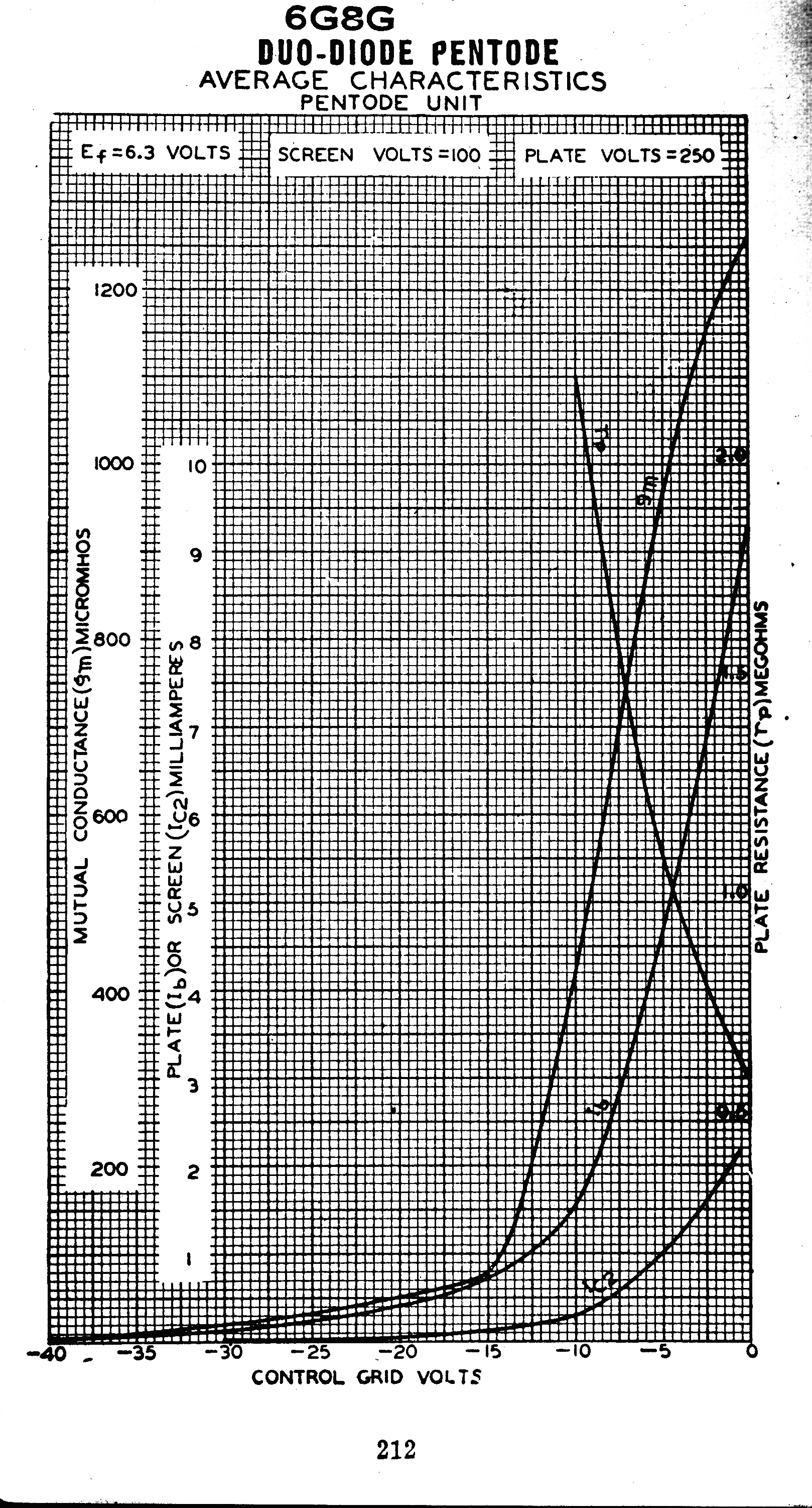
A classic example of this is shown in the curves for the 6G8 -- an Australian designed variable mu
RF pentode designed in the thirties.
For a square law response, ∂Ip/∂Vg (Gm) = kVg.
For the 6G8, the gm is a linear function of Vg over most of its range.
 In the early sixties a better solution to distortionless gain control with
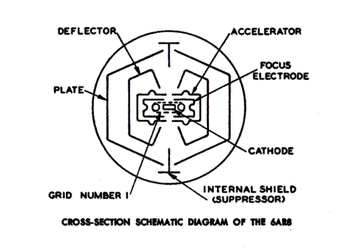
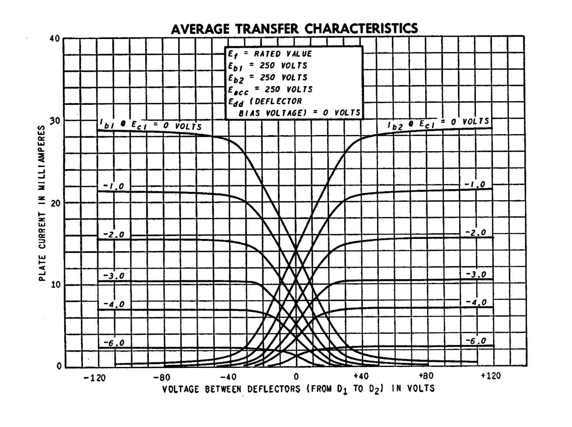
vacuum tubes appeared: the beam deflection tube: for example the 7360 or the 6AR8.
In the early sixties a better solution to distortionless gain control with
vacuum tubes appeared: the beam deflection tube: for example the 7360 or the 6AR8.
Here a rectangular beam of electrons is deflected linearly between a split anode.
A push-pull RF signal applied to the deflection plates produces a balanced push pull output.
The intensity of the beam, and hence the RF output, can be controlled by a grid driven by the AGC
voltage.
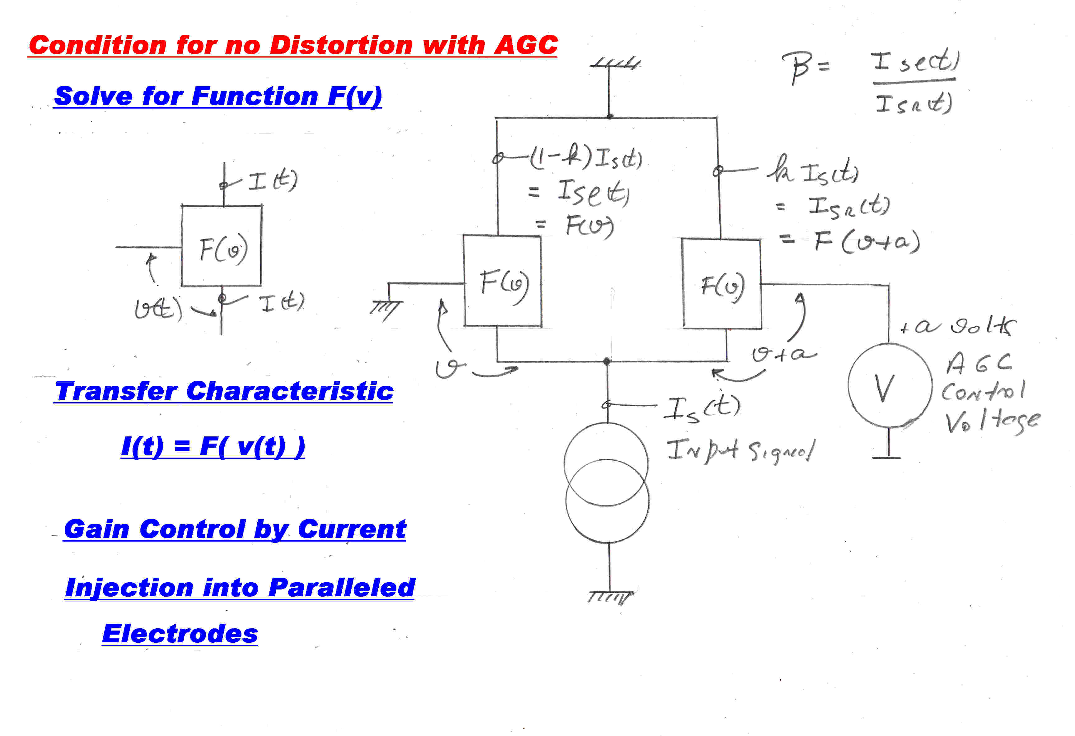 A signal current injected into the common electrodes of a long tail pair is normally
shared equally by both elements. The output ratio between the two sides, β , can be changed
by altering the bias on one side. This provides a mechanism for gain control.
A signal current injected into the common electrodes of a long tail pair is normally
shared equally by both elements. The output ratio between the two sides, β , can be changed
by altering the bias on one side. This provides a mechanism for gain control.
For no distortion the output ratio must be independent of the signal current.
It is necessary to find the transfer characteristic for the elements which fulfills this condition:-
Let the required transfer characteristic be:-
iout = f(vin)
OR i = f(v)
If we apply a bias voltage,a, to the right side , we have:-
il = f(v) and
ir = f(v + a)
The current ratio, β, then becomes:-
β = il / ir = f(v)/f( v + a )
Now v varies with the input signal Is(t),but we want the division ratio,
β, to be independent of the current, and so independent of v.
∴ dβ/dv = 0
∴ d[ f(v)/f(v + a ) ]/dv = 0
∴ (df(v)/dv)/( f( v + a) ) - [ f(v)/( f( v + a) )2]
[ df( v + a)/dv ] = 0
From which we get:
df(v)/dv/f(v) = df( v + a )/dv/f( v+ a )
for all values of a. So that:
df(v)/dv/f(v) = c ( a constant). So that:
df(v)/dv = c f(v) OR:
f(v) = ecv
THE ACTIVE ELEMENT SHOULD HAVE AN EXPONENTIAL TRANSFER CHARACTERISTIC
The transfer characteristic of a bipolar transistor is of the type:-
Icol = Io [ eVb/Vref - 1 ]
where Io and Vref are constants.
For working currents, eVb/Vref > > 1
So that:- Icol ≈ Io [ eVb/Vref ]
BIPOLAR TRANSISTORS HAVE THE REQUIRED EXPONENTIAL TRANSFER CHARACTERISTIC
Note: At low currents the control mechanism in vacuum tubes changes from charge control
to an energy barrier effect similar to that found in bipolar transistors. Electrons at
the high end of the Maxwellian distribution overcome the energy barrier of the negative grid
to provide a small plate current.
Although this effect provides the correct law for distortionless gain control, the currents
are usually too small to be useful for gain control in a tuner.
The dynamic response of integrated multipliers may now be good enough to provide gain control
in the RF/IF stages of a broadcast tuner.
The tuner was designed about thirty years ago when multipliers were not available.
The ultimate distortionless gain control element is the variable resistor.
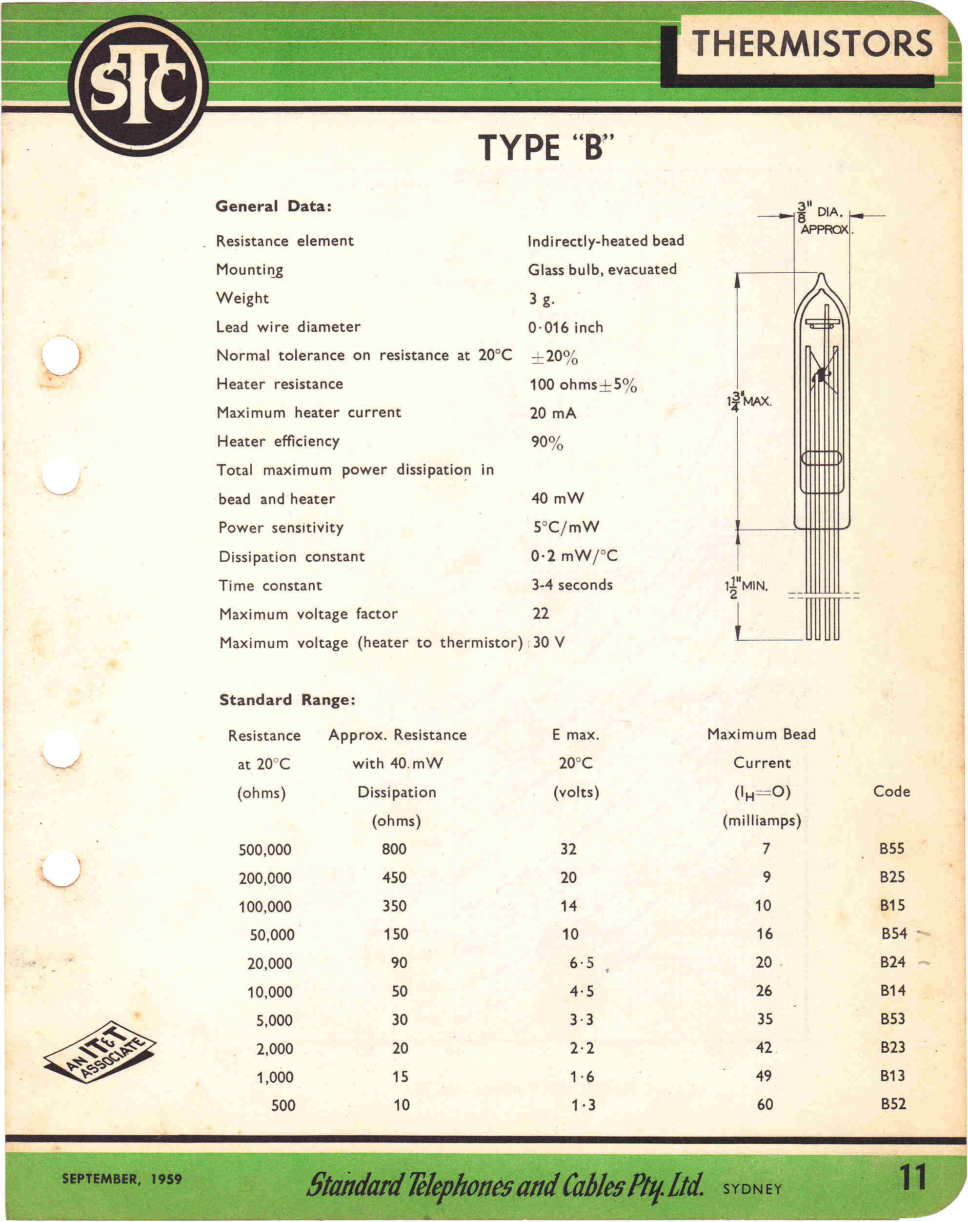 In a thermistor a heating element controls the temperature of a temperature sensitive resistor.
This can be used in a resistive divider or in a feedback loop to control the gain
over a wide range.
In a thermistor a heating element controls the temperature of a temperature sensitive resistor.
This can be used in a resistive divider or in a feedback loop to control the gain
over a wide range.
The dynamics of the thermistor as a control element are not attractive.
The time constants are of the order of 3 to 4 seconds. The thermal conduction delay between
the heating element and the variable resistor produces a non-minimum phase function.
This is highly undesirable in any feedback loop, especially in one which contains integrators.
Since the minimisation of distortion was one of the main design goals of the tuner design,
it was decided to adopt the thermistor as the gain control element and work around the
stability and dynamic problems.
All RF and IF stages employ heavy negative feedback to minimise distortion.
The bipolar transistors in the frequency changer are operated at a low current level to give an
exponential transfer characteristic for low modulation distortion as described above.
The stability problem is solved in the following way:-
[a] The AGC loop is split into two parallel paths - one path containing the thermistors
and a second path containg a fast gain control with no high frequency limitations.
This varies the local oscillator injection level into the mixer to control the
conversion transconductance. The time constants associated with this are many orders of
magnitude smaller than any encountered in the AGC loop.
It does not enter into loop stability.
NOTE: Although the three gain controlled stages are in series, the resulting
small signal control transfer function puts them in parallel.
Let each stage have a small relative increase in gain kn, so that the
output will be: [ 1 + kn ]sin(ωct)
For a number of controlled stages in series, the output will be:
[ 1 + ktot ]sin(ωct =
[ ∏( 1 + kn )]sin(ωct ),so, using the binomial theorem:-
ktot ≈ ∑kn ,that is all the changes in
cascaded stages ADD for small AGC corrections, and the transfer functions may be
taken to be in parallel.
[b] An integrator placed between the drive to the HF loop and the drive to the thermistors
ensures that, under steady state conditions, the HF loop drive will settle back to zero,
so that all the gain control resides in the thermistor loop.
The stability and dynamics of the overall AGC loop can be controlled by the ratio of gain
between the converter and thermistor loops.
[c] In this tuner the HF gain control is achieved by controlling the local oscillator
injection level in the frequency converter. This is operated under conditions to make the
conversion transconductance proportional to the injection level.
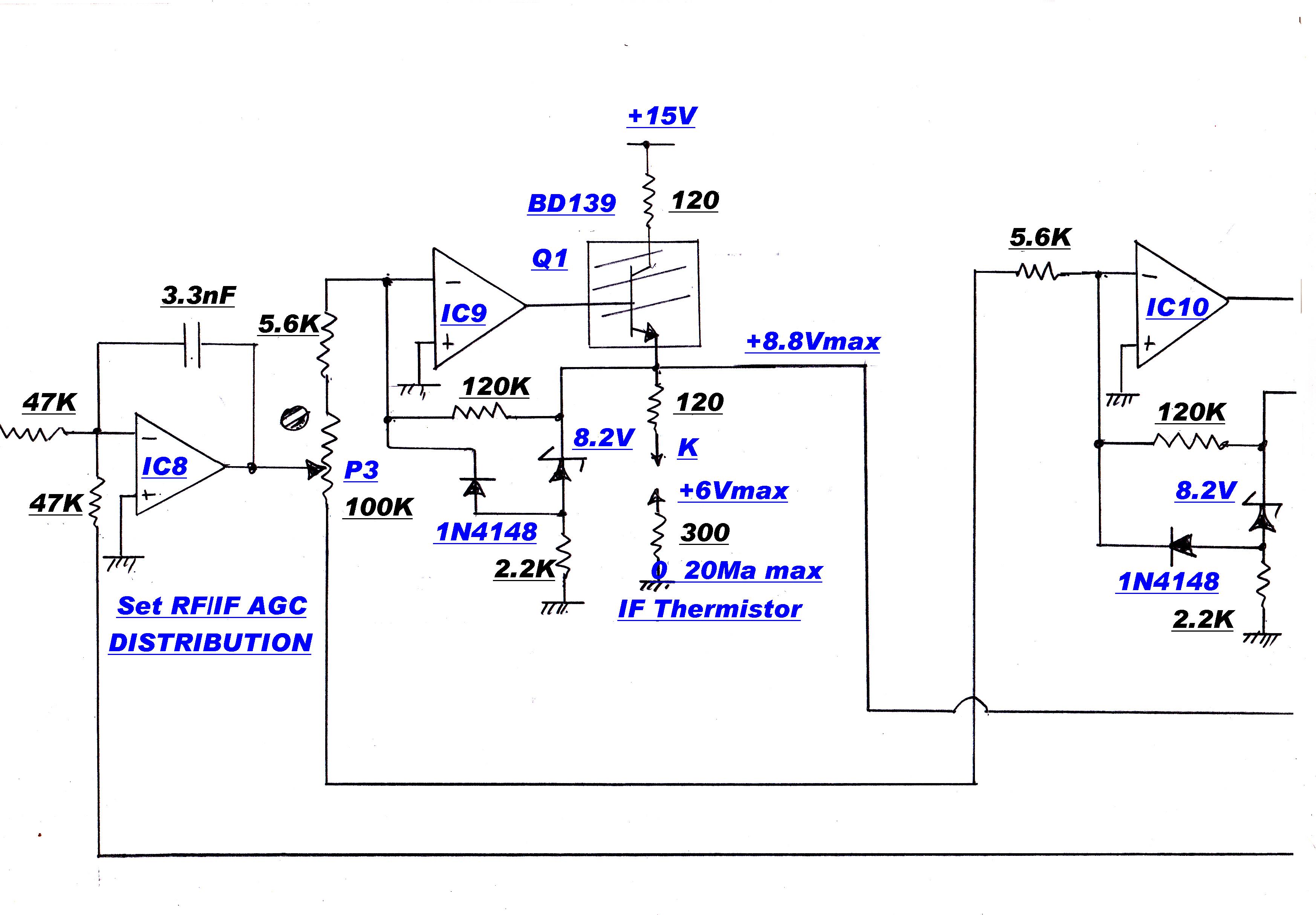
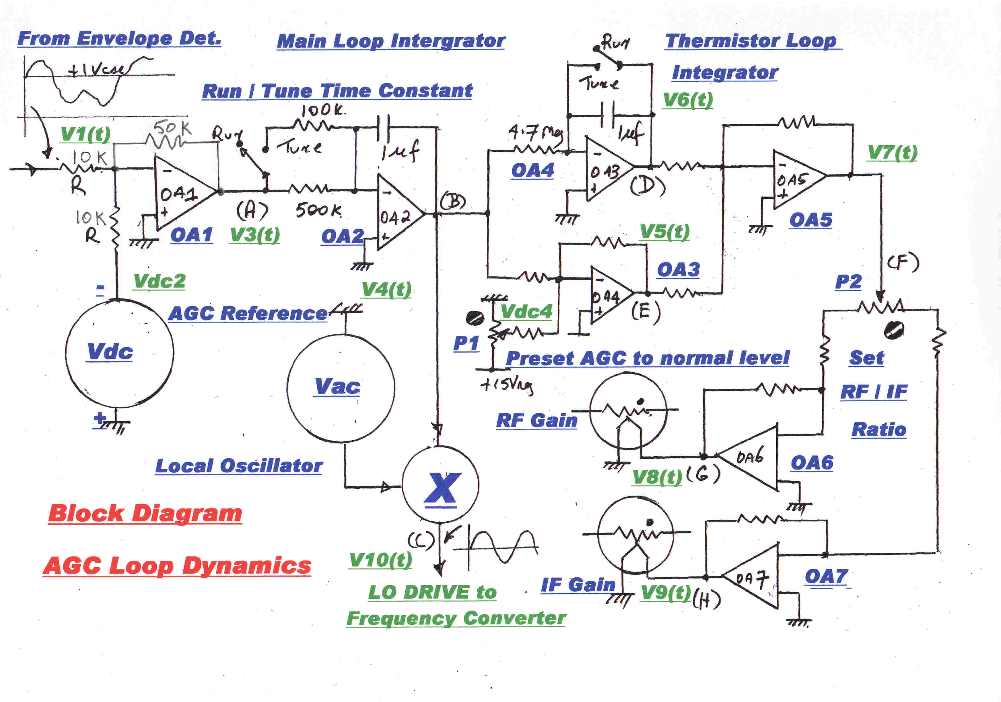 A simplified block diagram of the AGC is shown opposite:-
[1] The integrator OA2 forms the dominant stabilising pole in the AGC loop.
[2] It drives two loops in parallel:-
(a)The fast oscillator injection loop and
(b) The slow thermistor loop.
A second integrator,OA4,is included in the thermistor loop. This is disabled for the
"tune" condition. It is active during "run" and ensures that the DC value
of VB(t) = 0, that is, the injection level of the mixer is returned to the normal
operating value after a transient disturbance.
The mixer gain control operates only on transients.
[D] A preset voltage is added into the thermistor loop by P1.This sets the initial voltage on the
thermistors on turn on to be about the correct level for local stations. This minimises
the level of turn on transients and settling time in the loop.
[E] P2 sets the ratio of AGC between the RF and IF stages of the tuner.
[F] The time constant of the main loop integrator,OA2, is decreased during "tune"
This prevents large increases in audio output while the AGC loop is handling large
changes in signal input as the tuner is tuned through a carrier.
[G] The main loop integrator, OA2. ensures that the DC component of V3(t) is zero, so that
the carrier output from the envelope detector is exactly equal in magnitude to the AGC
reference voltage. The calibration of the modulation meters and alarms depends on this.
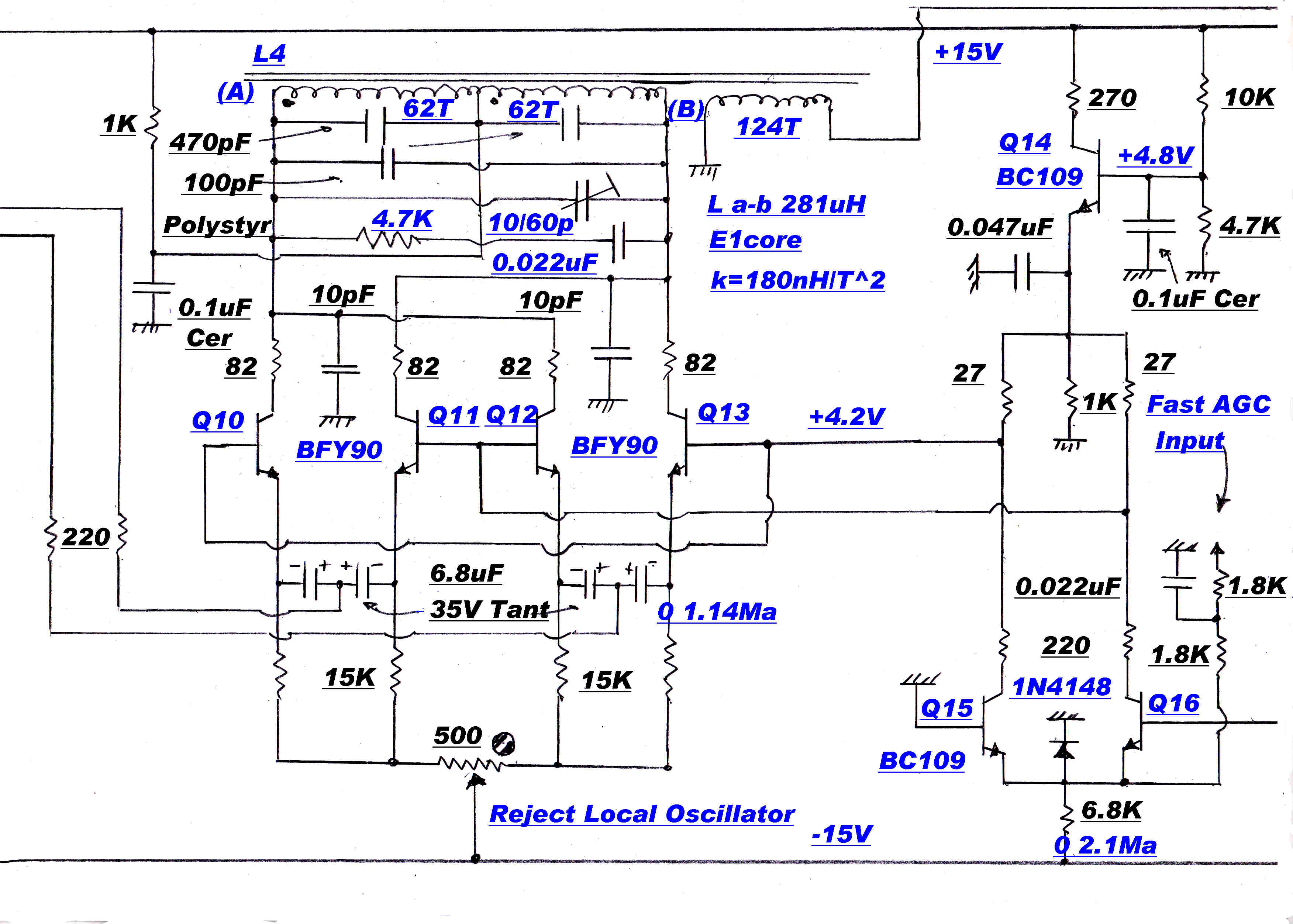
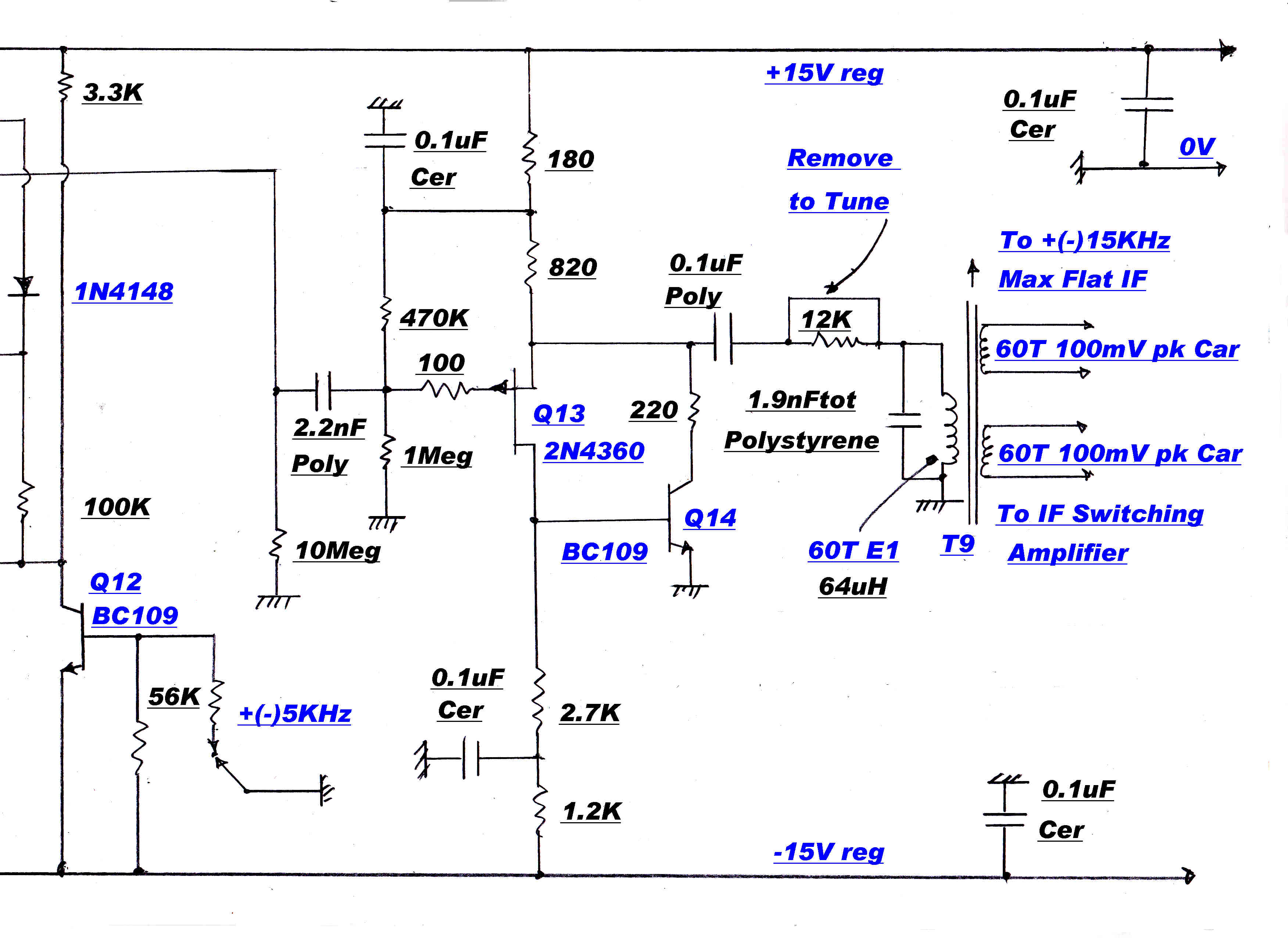
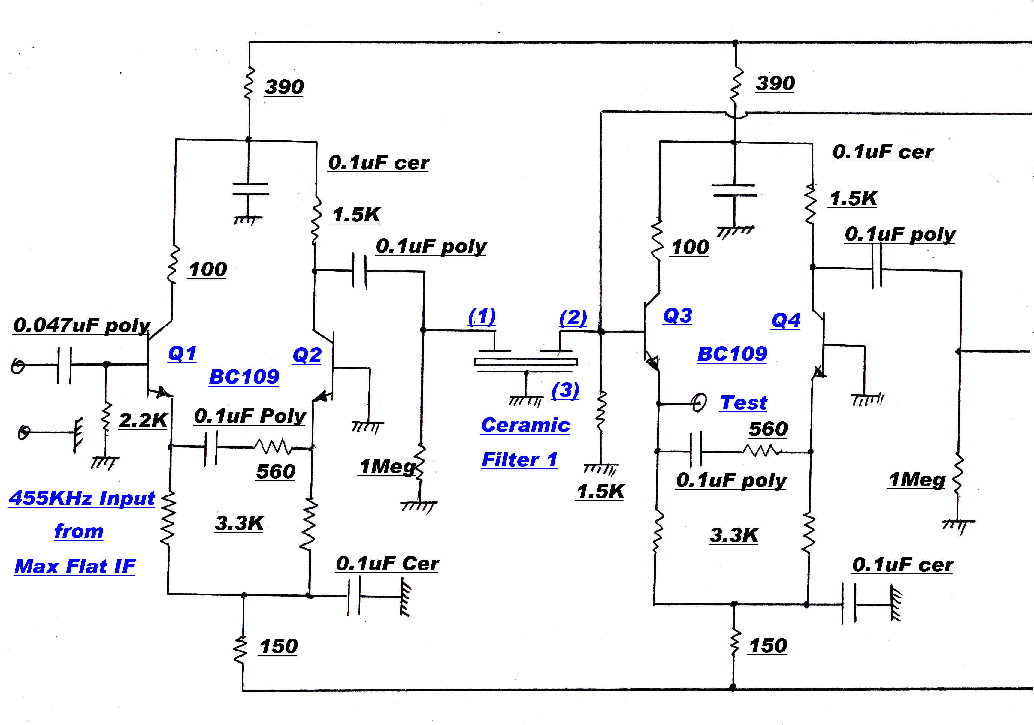
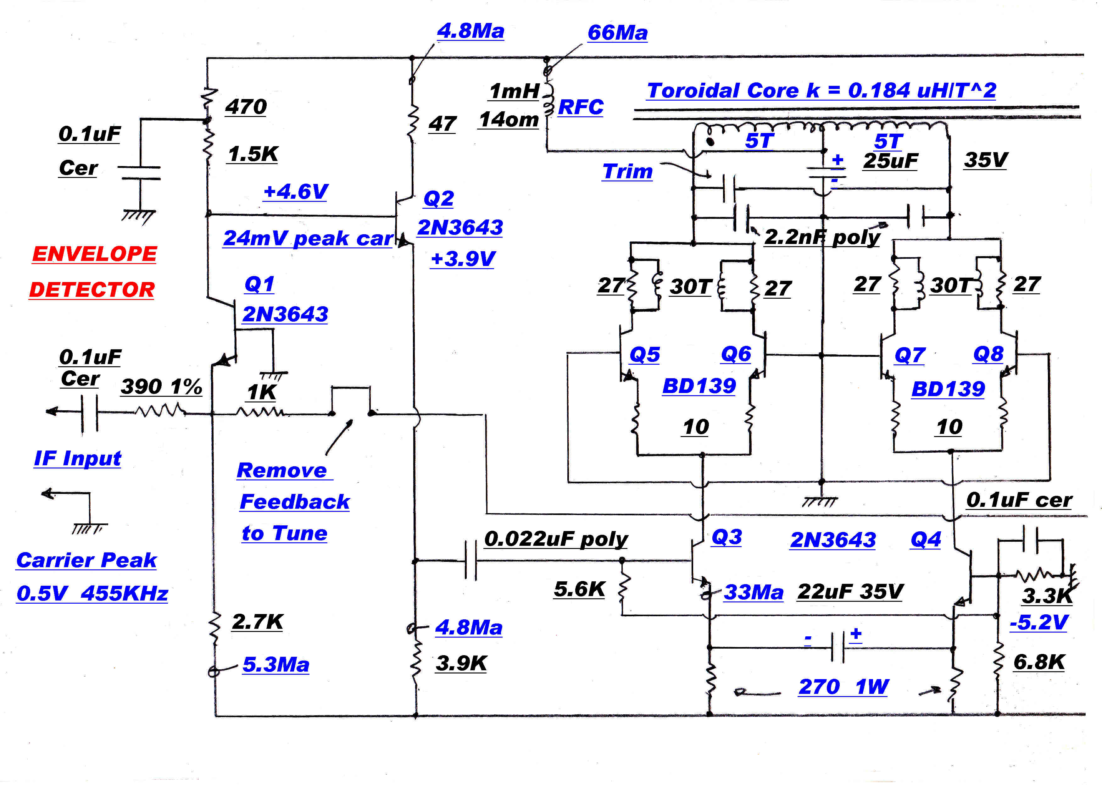
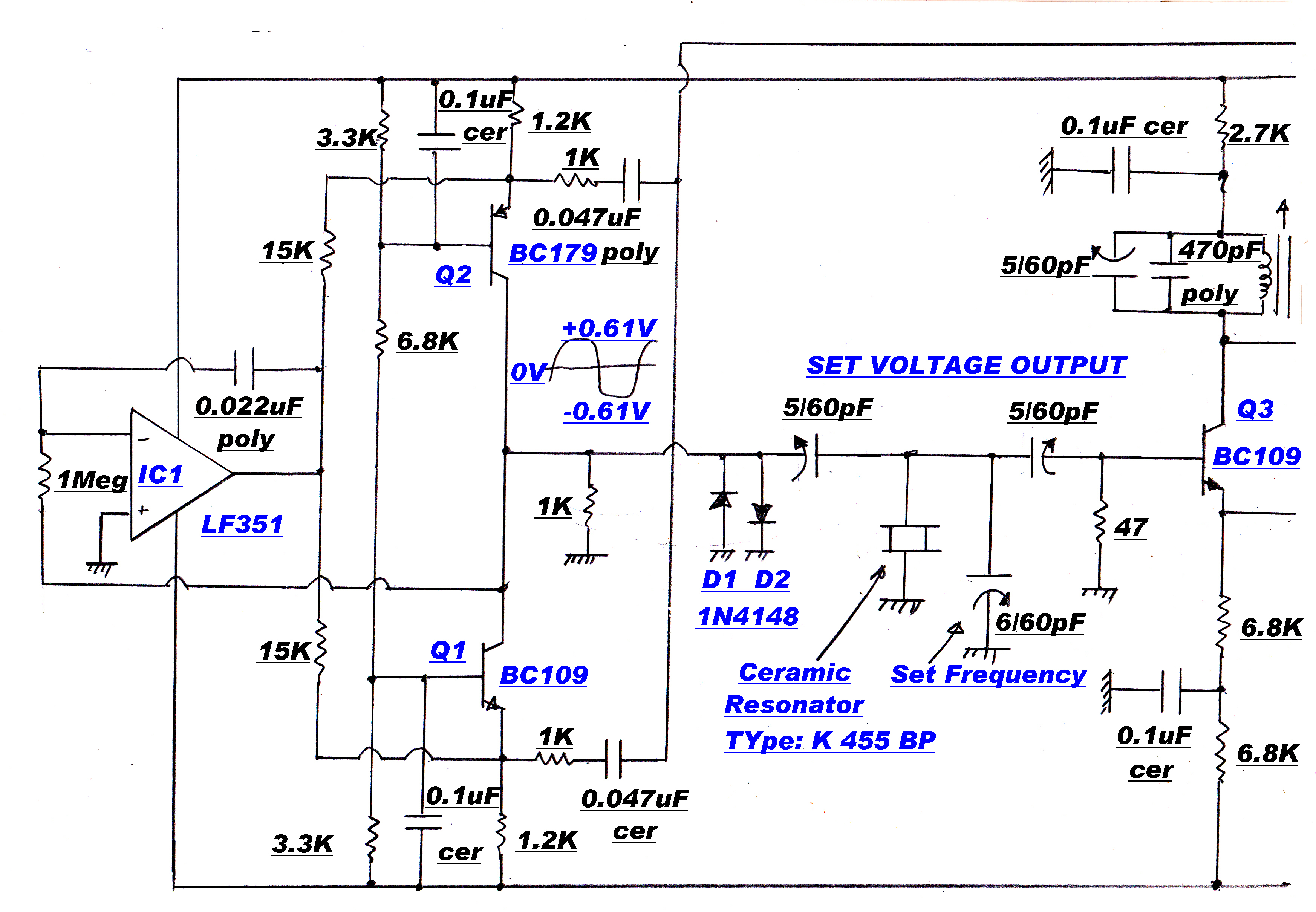
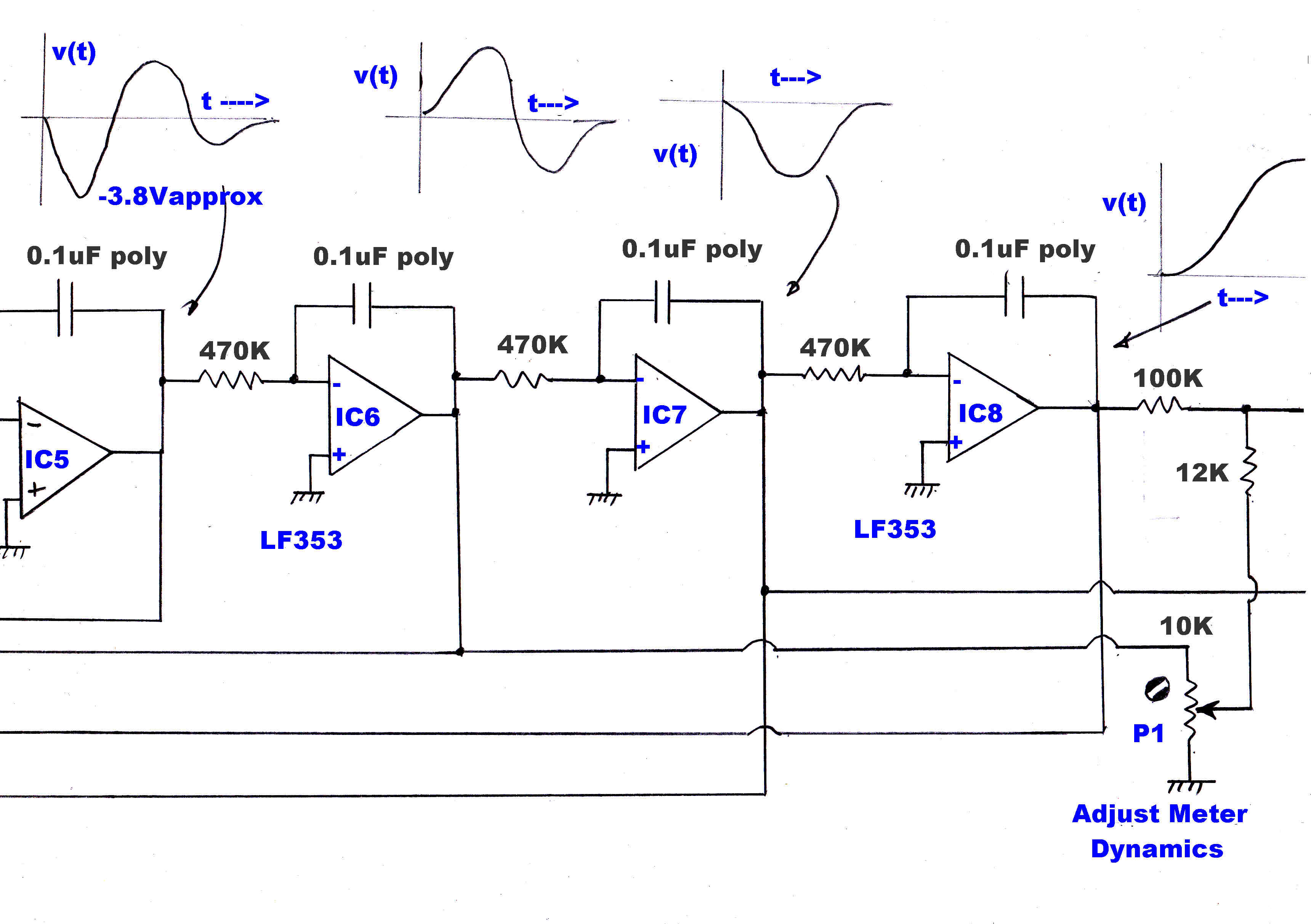
The gain controlled stage of the IF strip is shown opposite.
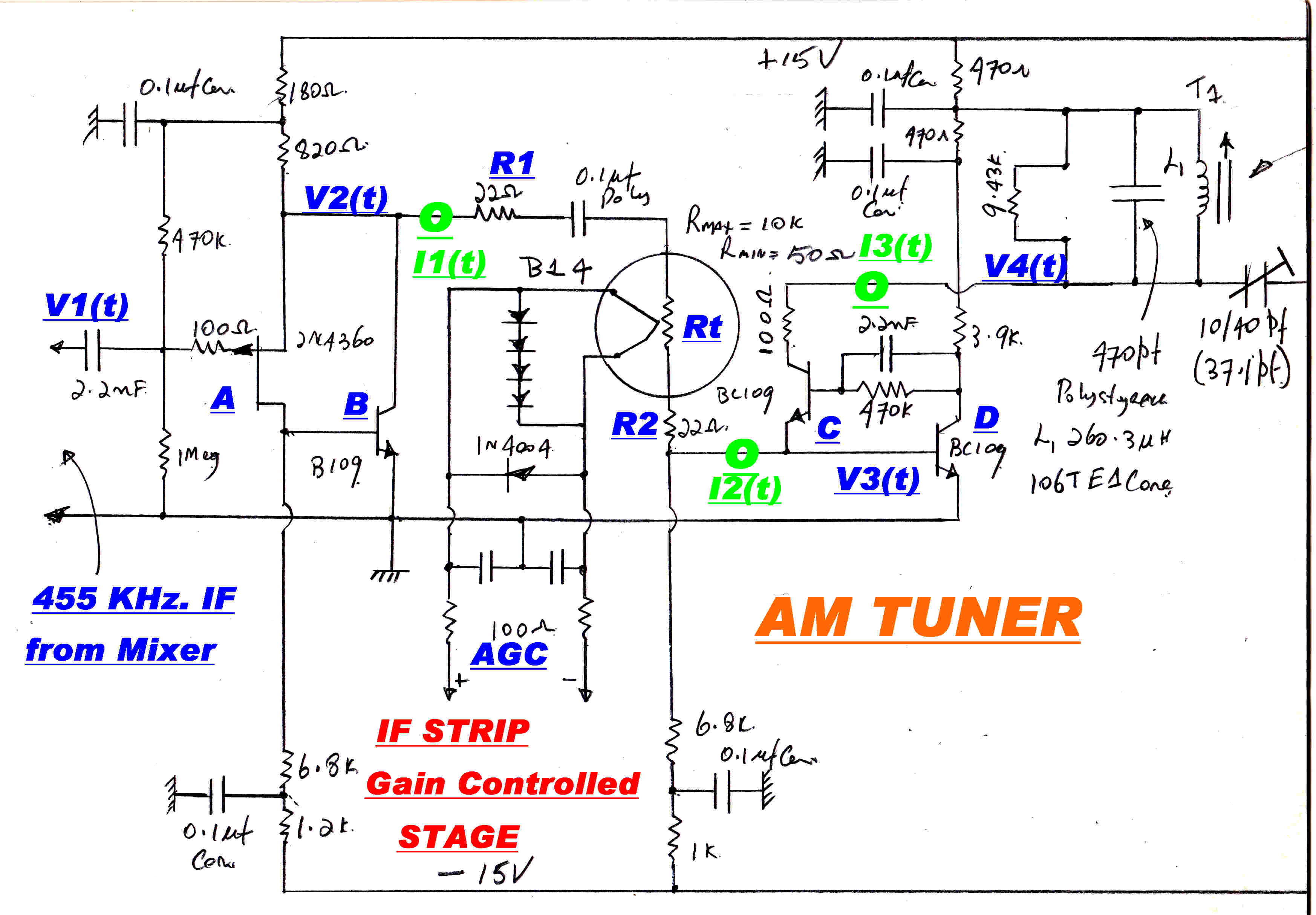 The high loop gain in the feedback pair A and B ensures to a high degree of approximation:-
V2(t) = V1(t)
Zout = 0
Similarly, for C and D :-
Zin = 0
I3(t) = I2(t) , so that :-
I3(t) = [V1(t)]/[ R1 + R2 + Rt ]
This is the gain control function for the stage.
Because of the very high degree of feedback on the active elements, the modulation distortion
produced by the stage is close to zero.
The nominal cold resistance of the thermistors is 10kohms: the minimum resistance with
20Ma heater current about 50 ohms.
Substituting in the above equations the control range should be:-
Control range = 20log[ ( 22 + 22 + 10k )/( 22 + 22 + 50)] = 40.6 db
Since two stages are under gain control, the input signal range should be 80db.
For the thermistors used, the measured value was 70db.
The minimum input signal for AGC control is 142uvolts: the maximum signal about 0.5volts.
This greatly exceeds the expected variation in signal strength from a group of
AM stations servicing an area on ground wave.
The IF stage gain plotted against the thermistor input current in milliamps
is shown opposite.
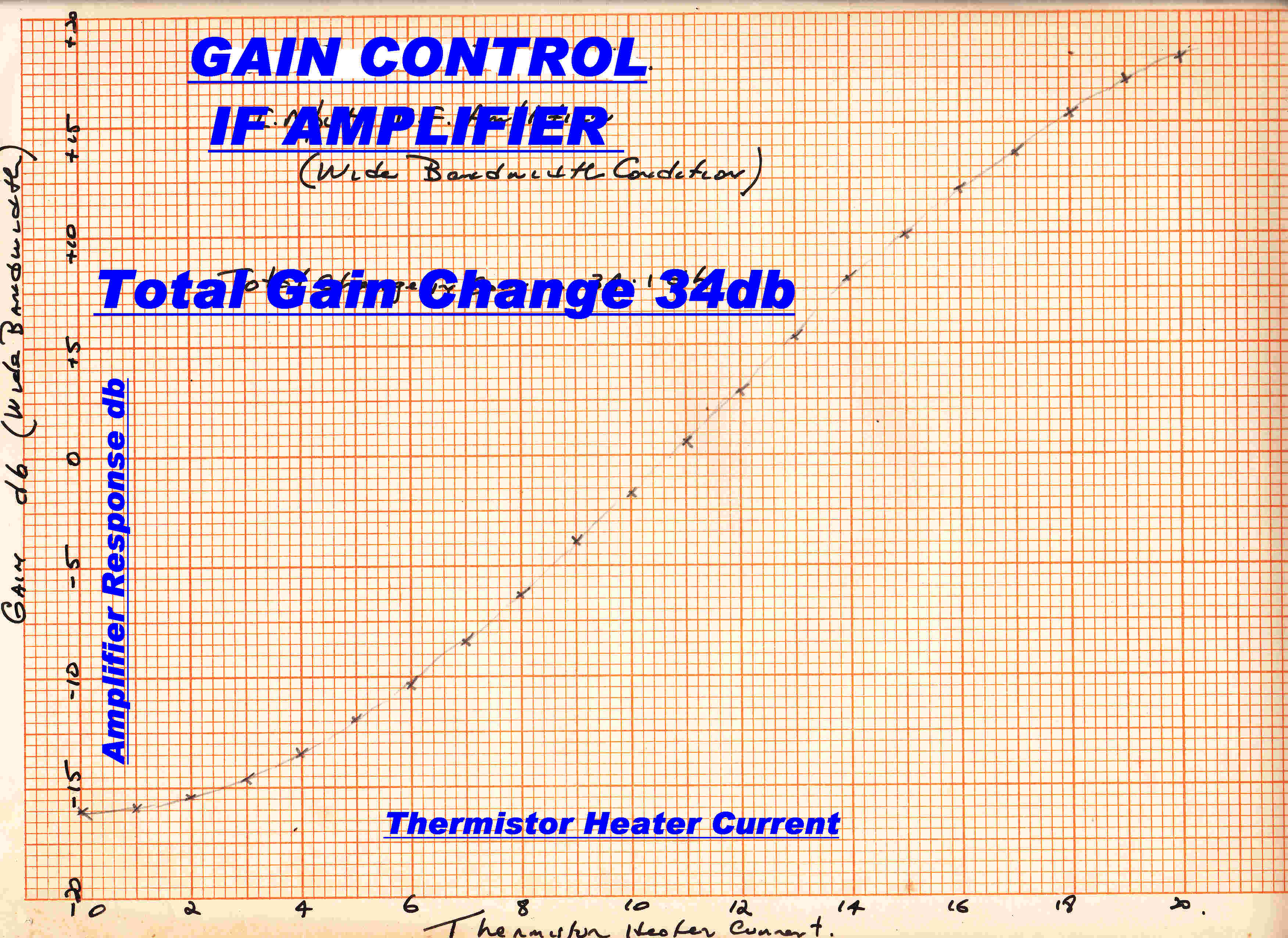 The control is approximately logarithmic.
The S meter is driven by the sum of the thermistor heater currents, so it follows a
logarithmic law.
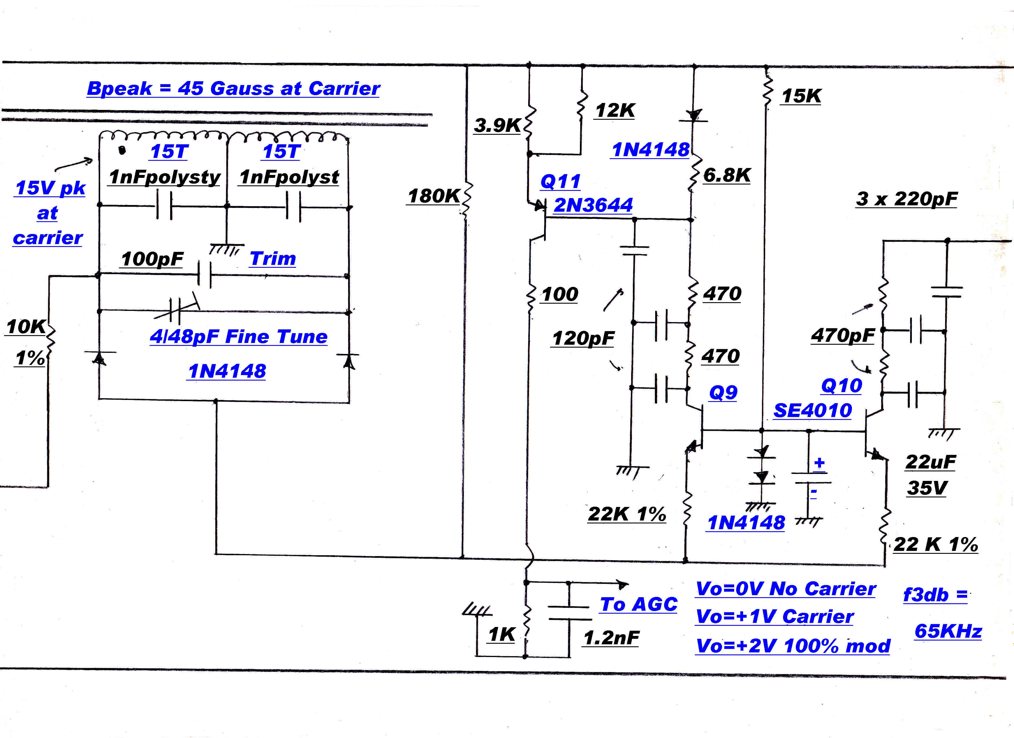
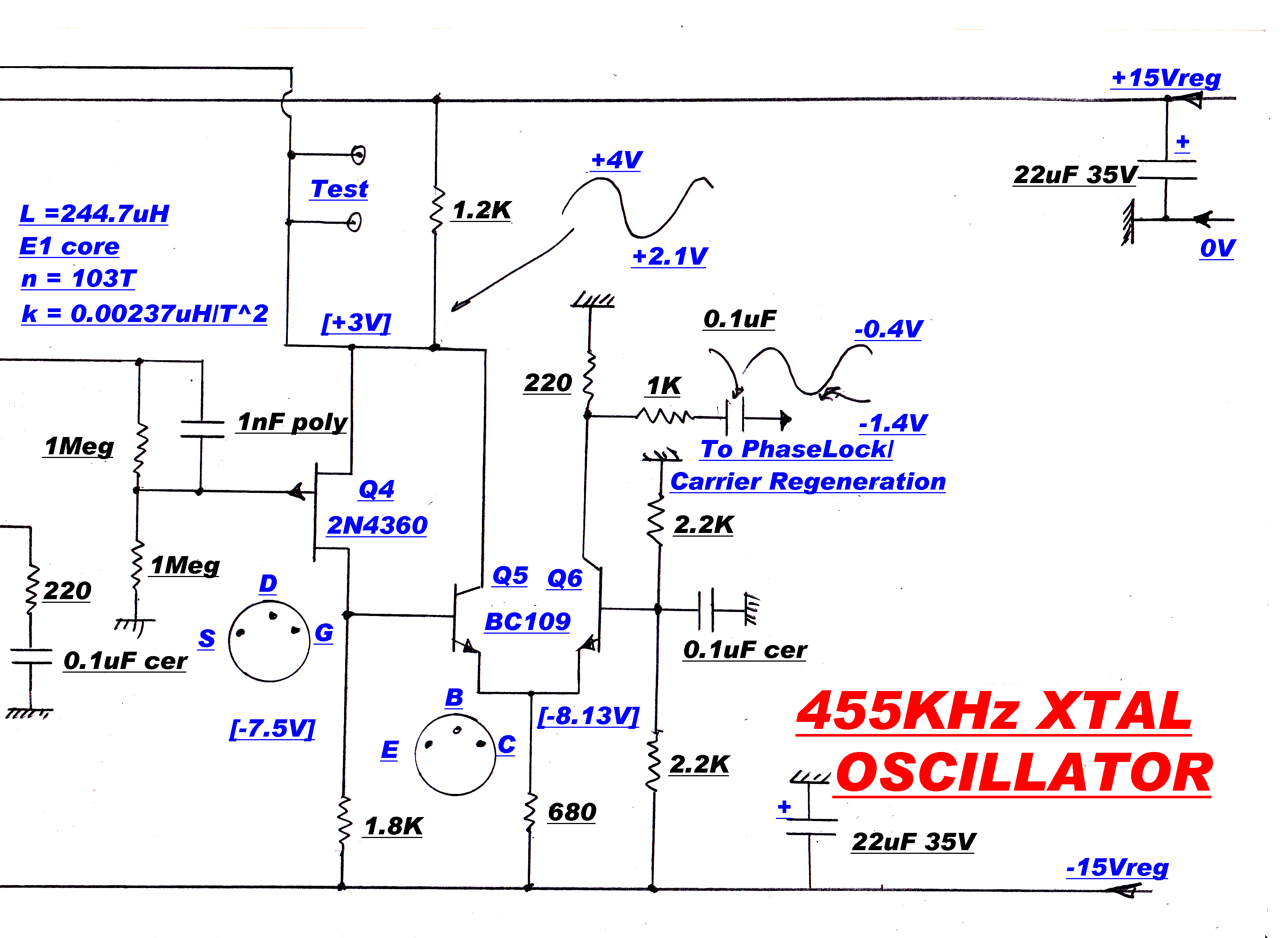
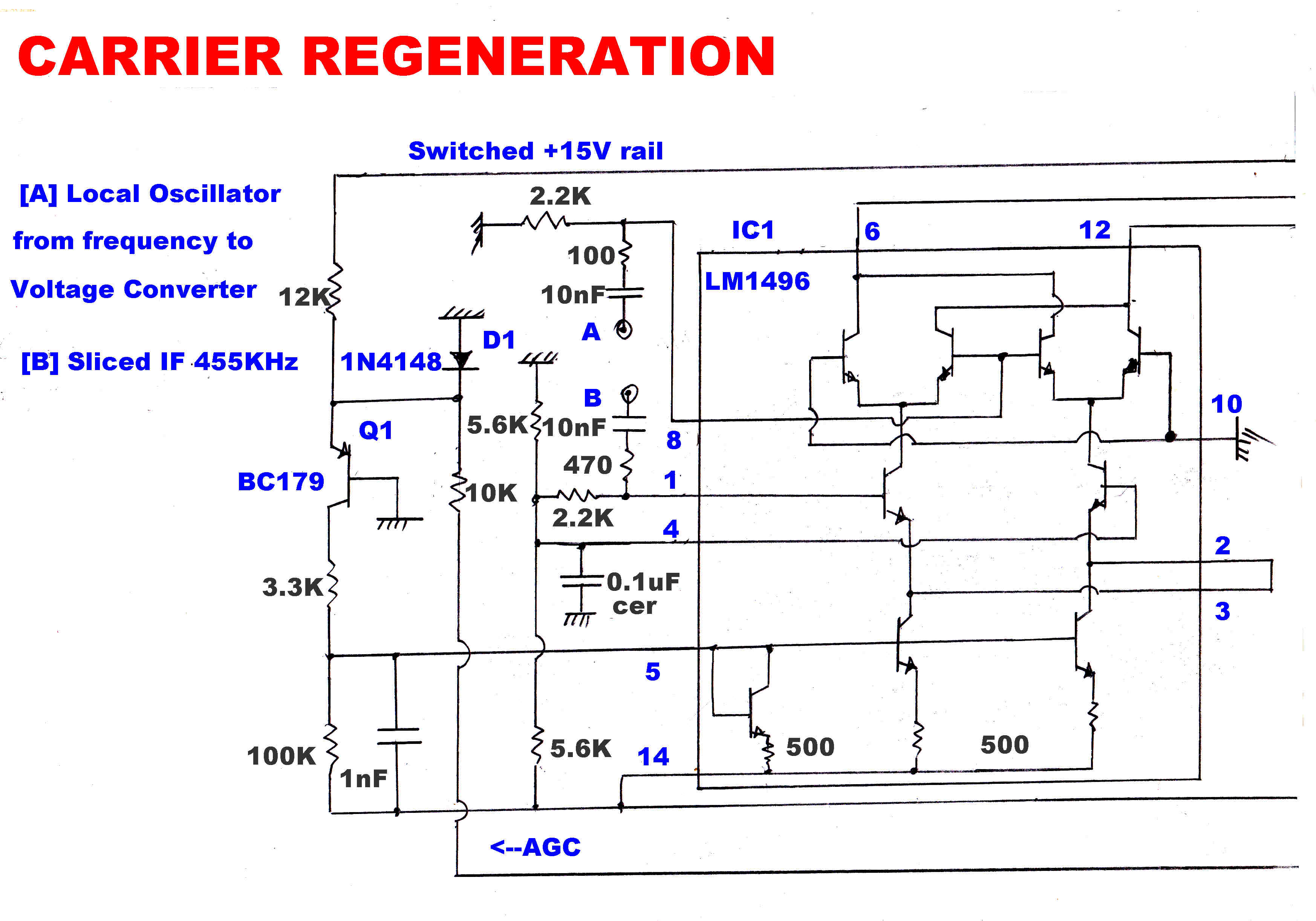
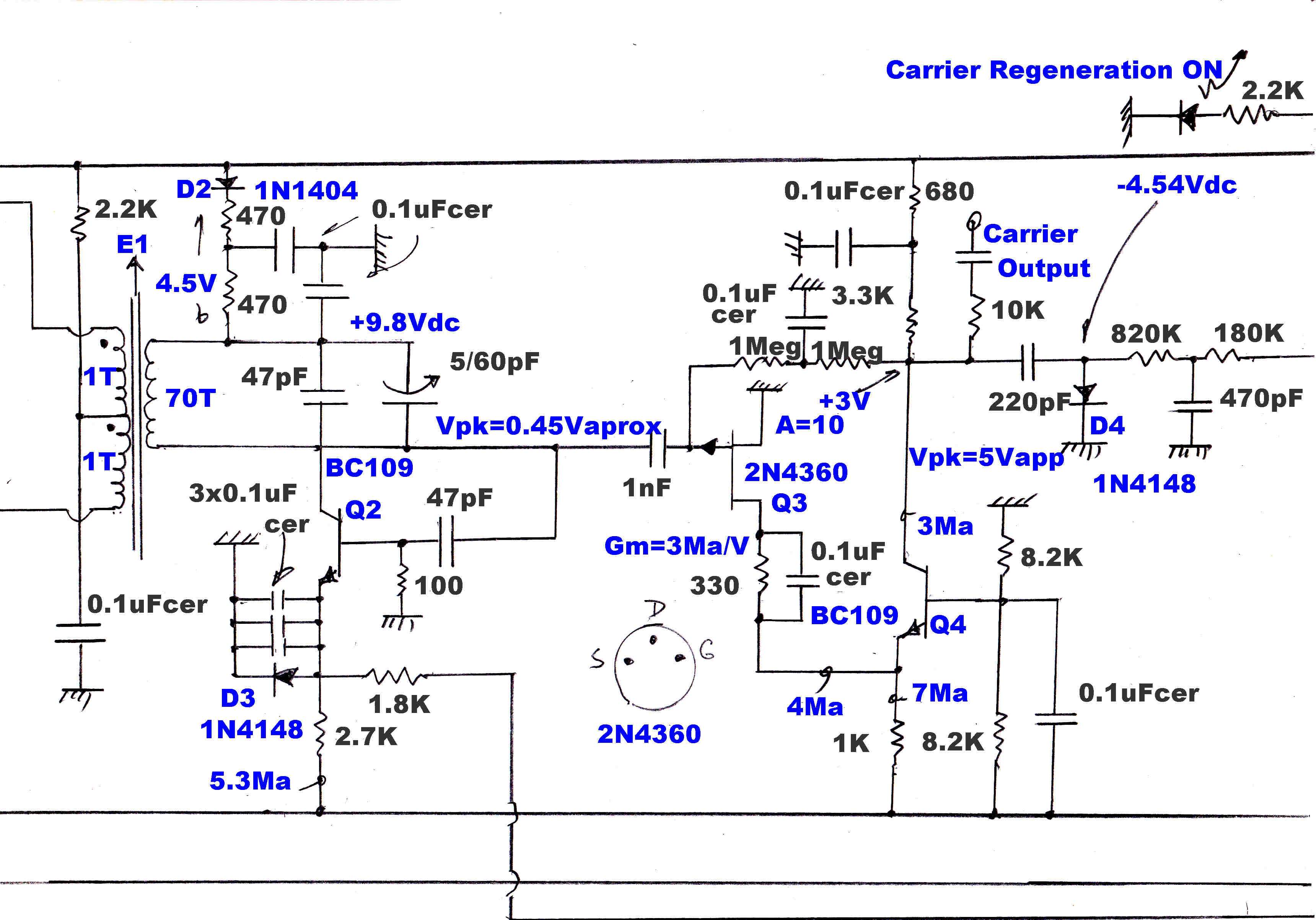
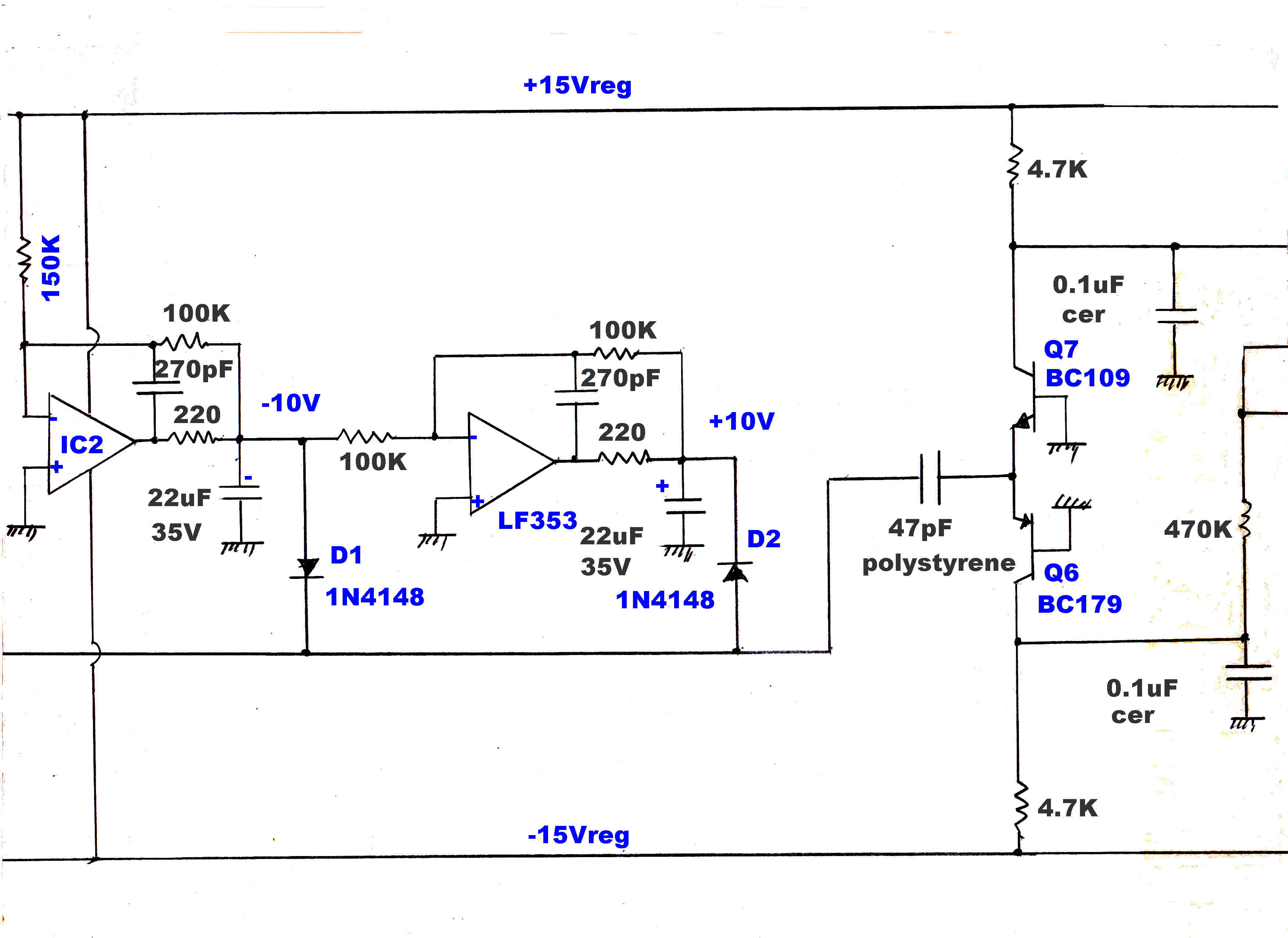
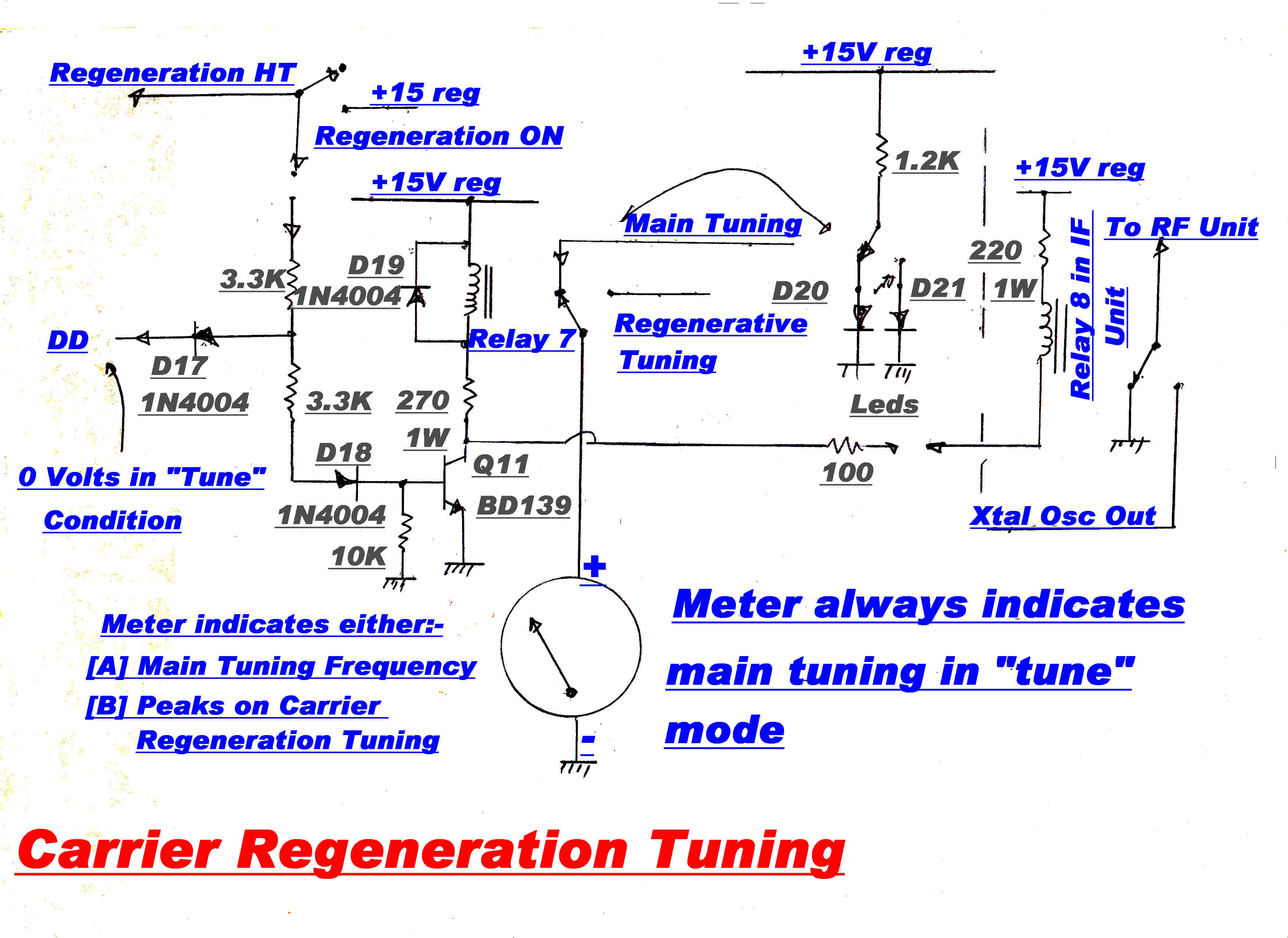
The carrier must be regenerated as a reference for the product demodulators.
This is performed by a phase locked loop.
In a conventional receiver a variable frequency oscillator is locked to the output
frequency of the IF strip.
In this receiver, in the "run" mode, the local oscillator frequency driving the
frequency changer is controlled, so that the IF output is phase locked to a 455KHz. crystal
oscillator. This ensures that the IF carrier is always centered in the IF strip - there
can be no mistuning.
The carrier injection into the quadrature detector must be exactly 90 degrees out of
phase with the IF output. Small errors can introduce a significant in-phase
component and mask the small quadrature component.
For a phase error, φ , the output from the quadrature detector Vq is:-
Vq = Ipsin(φ) +Iqcos(φ)
If Vq ≡ Iq then:
φ ≡ 0 since usually Ip >> Iq
An extra slow speed integrator loop was introduced to ensure this condition.
The block diagram for the phase locked loop is shown below:-
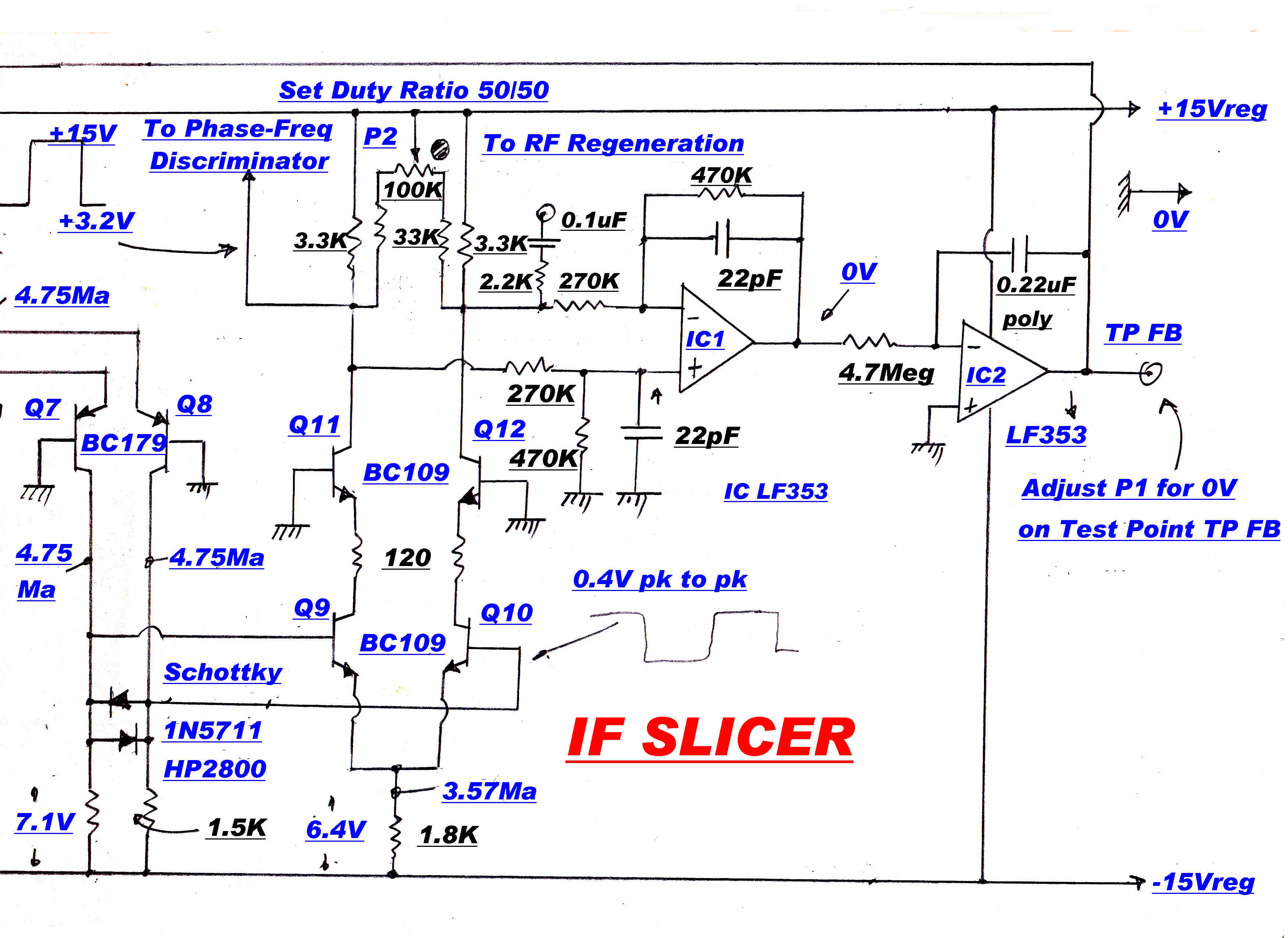
Modulation is stripped from the carrier by a "slicer".
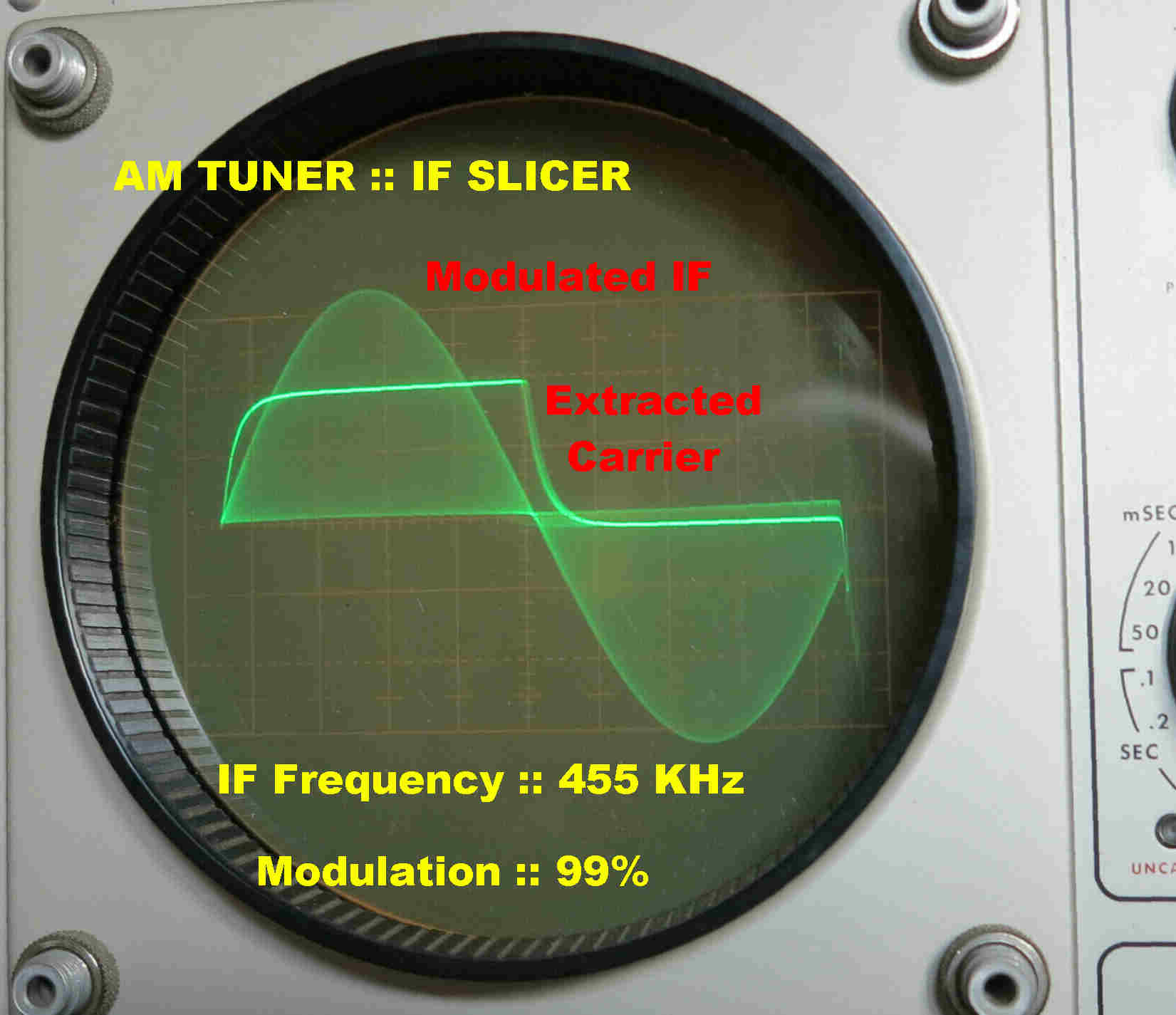 This is a high speed DC coupled amplifier
with severe limiting in both positive and negative directions. A high gain slow speed DC
loop centres the amplifier, so that the clipping is about zero volts and the output
always has a 50/50 duty ratio.
This is a high speed DC coupled amplifier
with severe limiting in both positive and negative directions. A high gain slow speed DC
loop centres the amplifier, so that the clipping is about zero volts and the output
always has a 50/50 duty ratio.
The square wave output produced by an AM signal modulated to a depth of 99% is
shown opposite:-
The amplitude and phase are independent of modulation.
This square wave carrier - stripped of modulation - and the output of the reference 455KHz.
crystal oscillator are applied to a digital frequency/phase discriminator. When the inputs are
out of phase lock the discriminator produces an error of the correct sign to pull the IF output
towards the Xtal frequency. After phase lock, the system acts as a linear phase
discriminator with zero output when the two inputs are in phase.
In the original design the quadrature carrier reference was derived from the in-phase carrier
with a -90 degree RC phase change network. The long term stability was inadequate to maintain
the required acccuracy of the quadrature injection.
A new system was developed to make the 90 degree injection angle inherent
in the circuit-- wthout any adjustments or "tweaks".
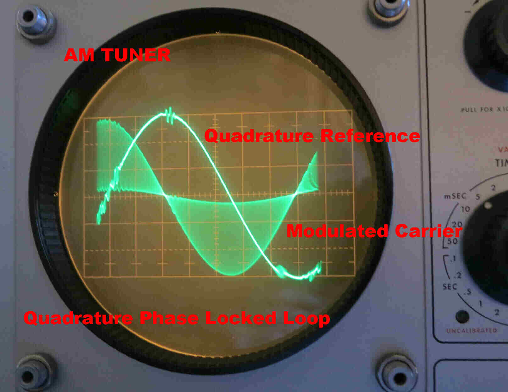 A phase sensitive rectifier ( product demodulator ) produces zero output when the two inputs
are in quadrature. The modulated output from the IF amplifier and a reference 455KHz. from
the Xtal oscillator are applied to a phase sensitive rectifier. The output is then integrated
and introduced as an error in the phase locked loop. Because of the integrator action its
output will eventually dominate all other inputs to the loop. Long term, the integrator
input must be zero - th output of the phase sensitive rectifier zero - and the two carriers
90 degrees apart.
A phase sensitive rectifier ( product demodulator ) produces zero output when the two inputs
are in quadrature. The modulated output from the IF amplifier and a reference 455KHz. from
the Xtal oscillator are applied to a phase sensitive rectifier. The output is then integrated
and introduced as an error in the phase locked loop. Because of the integrator action its
output will eventually dominate all other inputs to the loop. Long term, the integrator
input must be zero - th output of the phase sensitive rectifier zero - and the two carriers
90 degrees apart.
A -90 degree RC phase change network is placed between the Xtal oscillator and the
phase sensitive rectifier. Adjusting the phase change through this network changes
the oscillator phase, and so the in-phase injection derived from it.
The two inputs to the phase sensitive rectifier are shown in the oscillogram.
The transients on the sinusoid are induced into the earth loop of the CRO probe by nearby
digital circuitry in the phase/frequency discriminator.
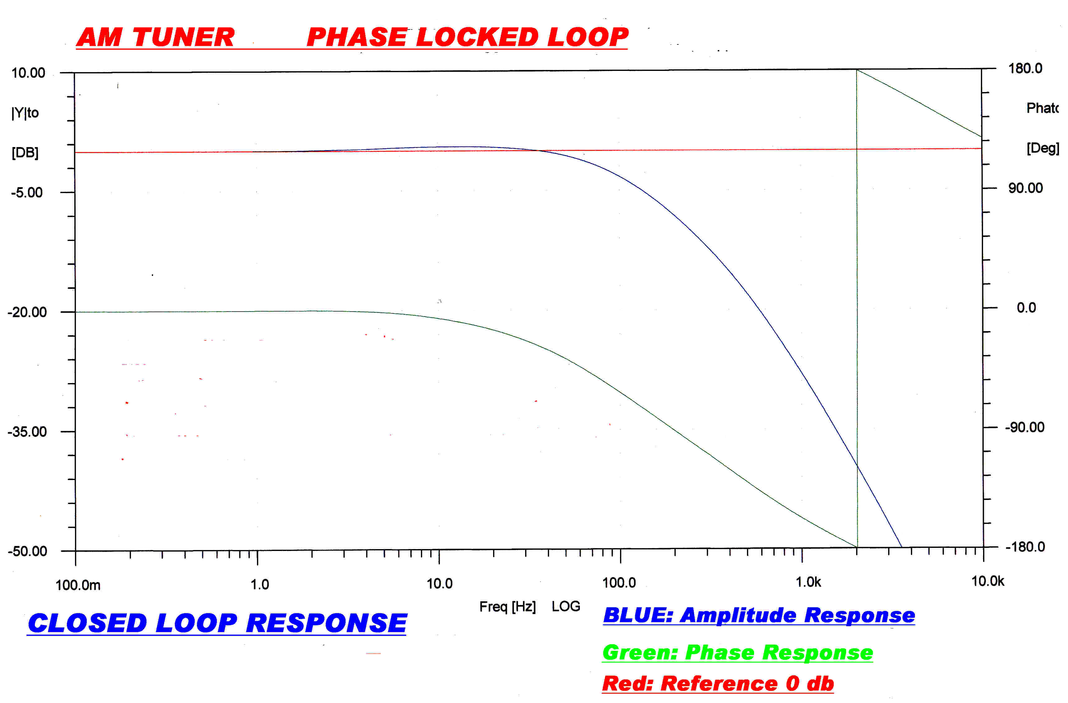
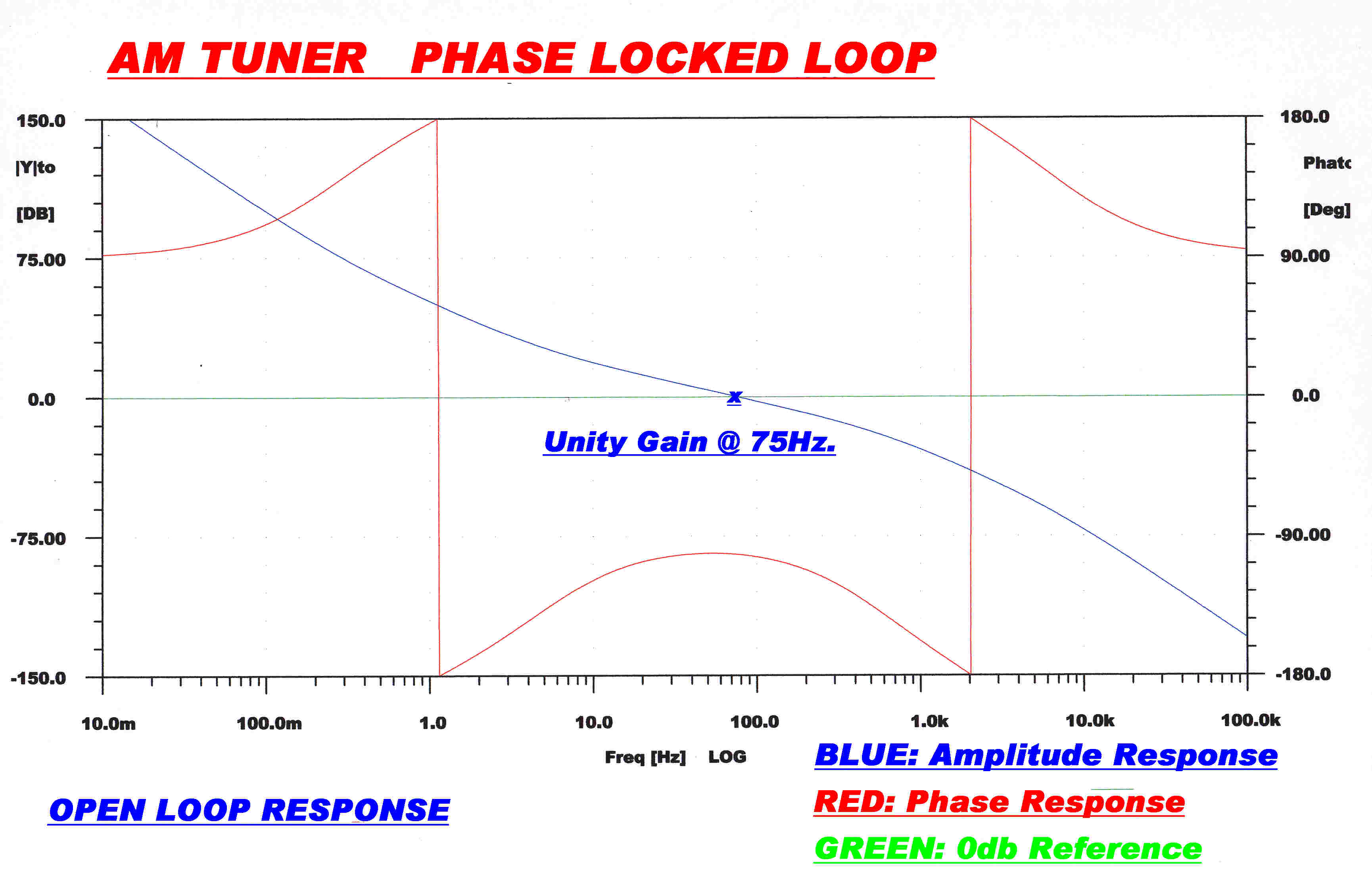
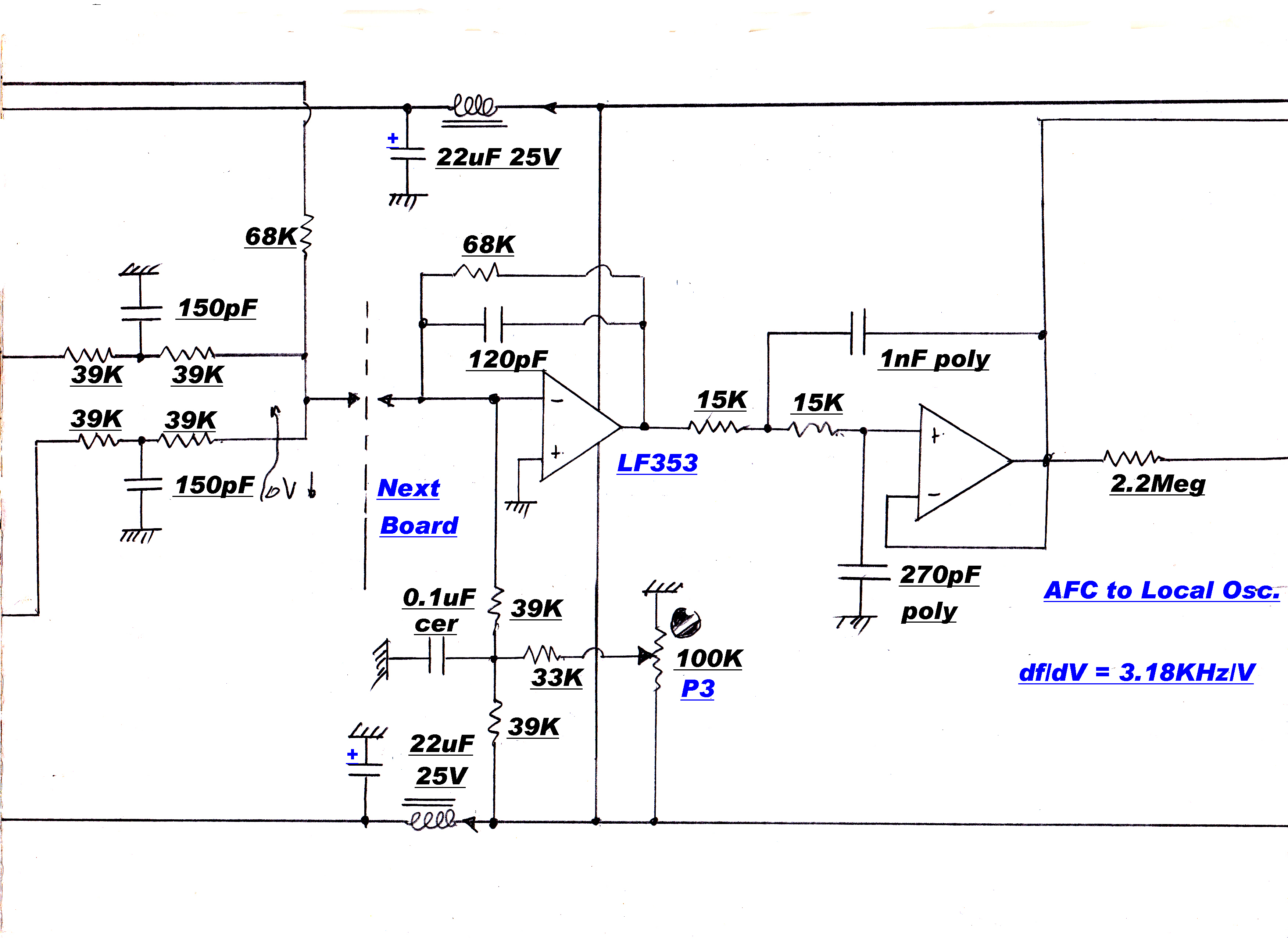
The open and closed loop response of the PLL loop is shown above.
A frequency controlled oscillator acts as a phase integrator, so the loop effectively has three
integrators in series. This leads to an ultimate open loop phase change at low frequencies
of 270 degrees.The unity gain open loop frequency is 75Hz. giving a closed loop cutoff frequency
of about the same value.
The phase modulation output is taken from OA1. This output is forced to near zero when
the loop is active, that is below 75Hz. Above this frequency it follows the output of the digital
phase/frequency discriminator. Effectively, then, the phase output is AC coupled with a
low frequency cutoff of 75Hz.
Phase modulation between 75Hz. and about 1KHz. is usually produced by a non-linear mechanism
within the transmitter. Above this frequency asymmetry in the passband of matching networks
and radiators usually produces phase modulation.
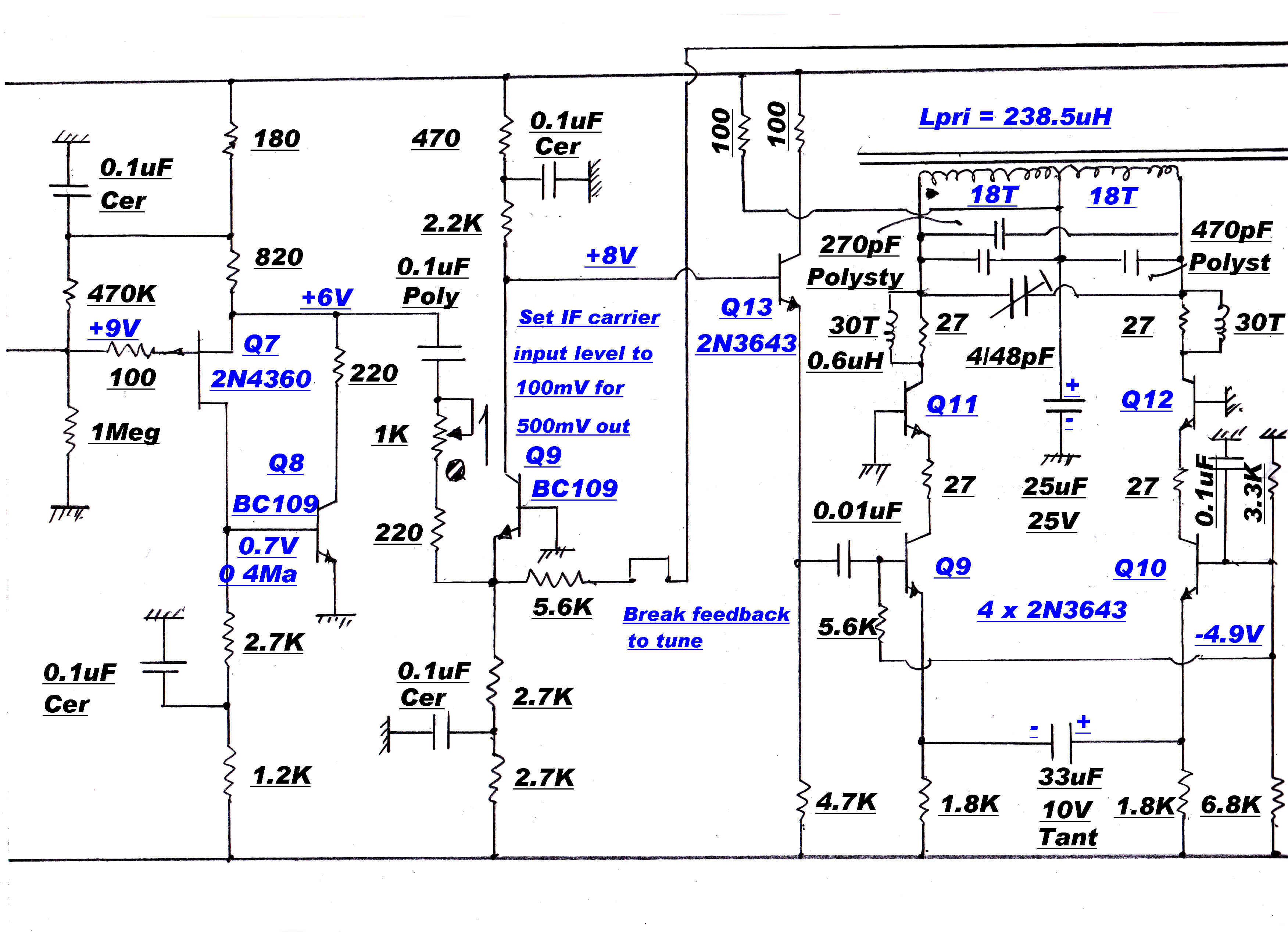
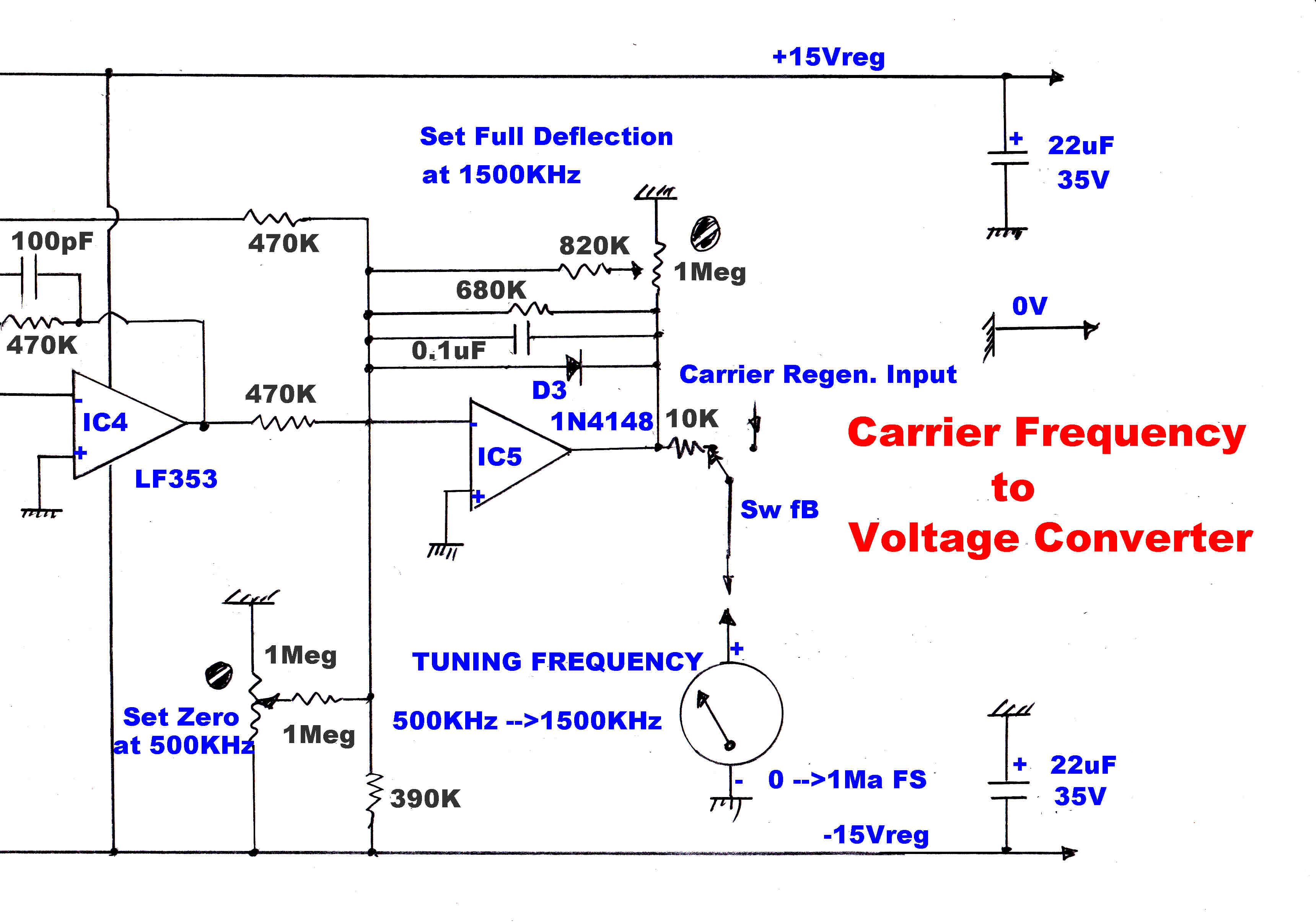
The IF - stripped of its modulation - is remixed with the local oscillator to give the input carrier. This is brought out to the front panel for direct measurement of the input frequency.
The tuner is designed as a test instrument.Therefore its response should be flat
and phase linear across the audio band say - 15KHz.
To achive good transient response with minimum overshoot, the flanks on the response of the RF and
IF networks should not be too steep.
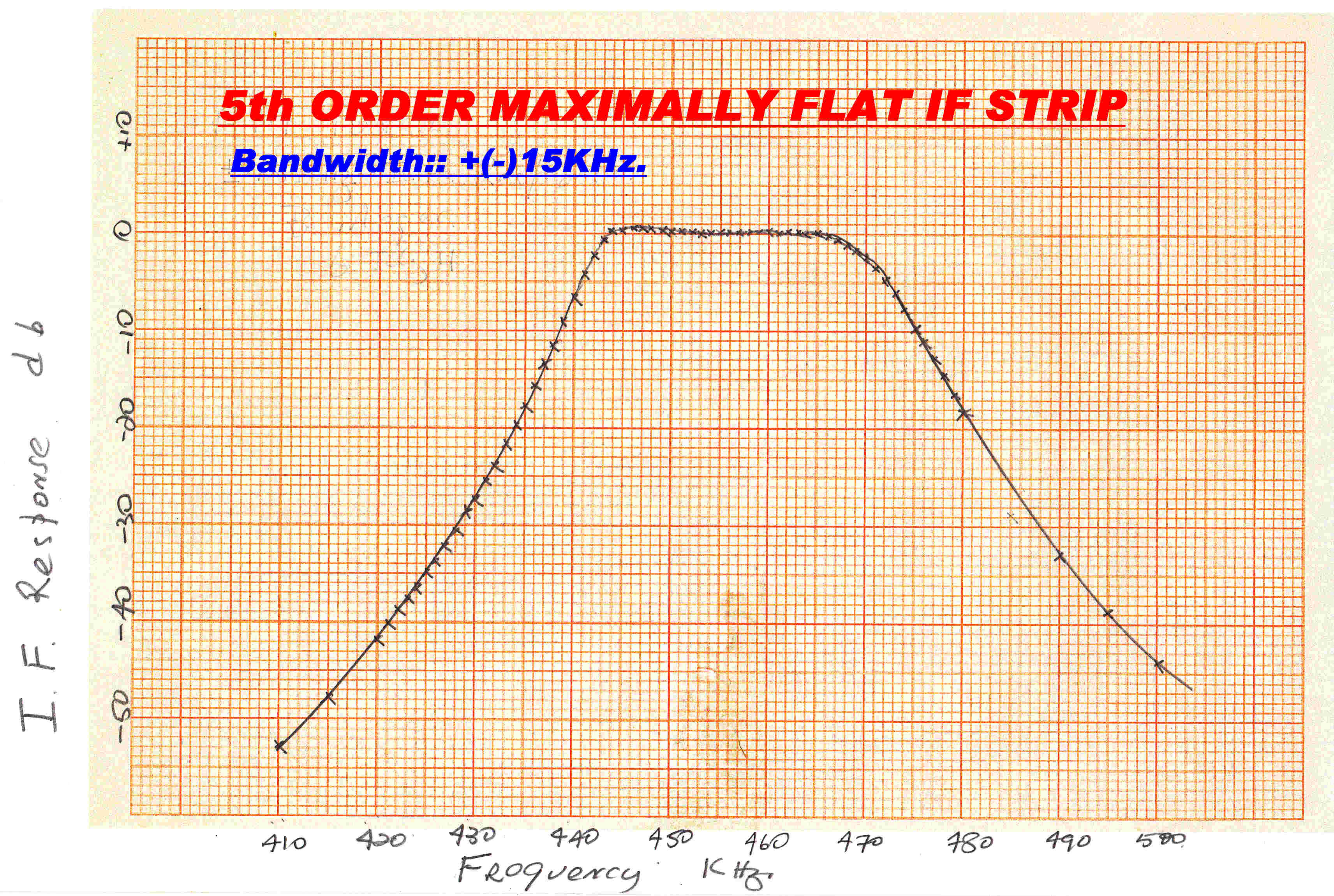
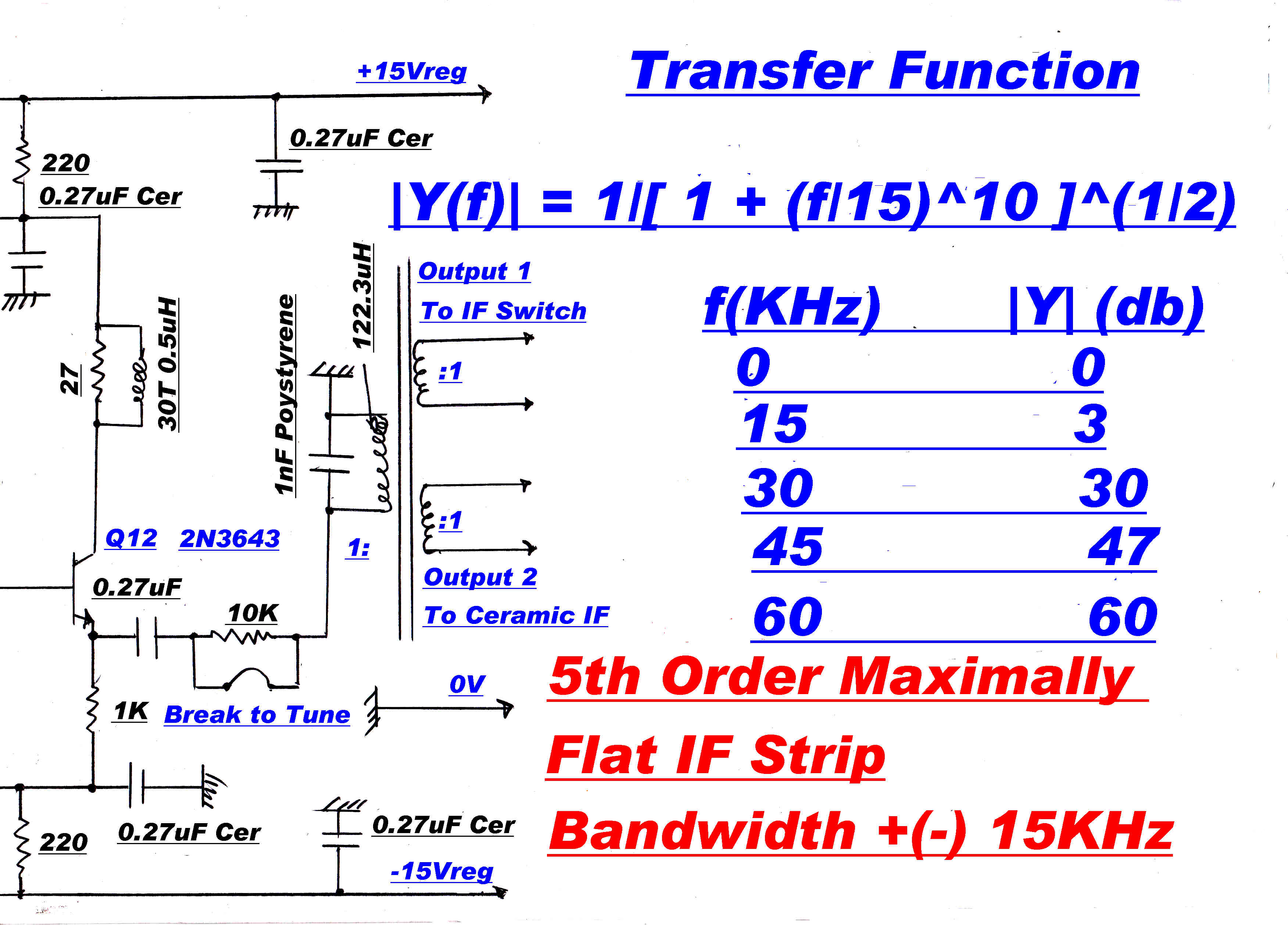
To cover situations where extra selectivity is required, a 15KHz 5th order maximally flat IF
and a ceramic filter with a very sharp cutoff at 8KHz can be added in cascade with the basic IF.
The response required in the RF and IF amplifiers can now be estimated:-
[A] RF NETWORKS -- RF INPUT AMPLIFIER and CONVERTER
The input RF amplifier has two circuits tuned by the main three ganged tuning capacitor.
Since these must track from 550KHz to 1500KHz, they take the form of simple resonant LC tuned circuits.
Referred to base band these each have one pole on the real axis. The output network in the collectors
of the converter forms another pole. If all three poles are made coincident, the overall response will
approximate Gaussian and phase linear.
Note:- Precautions must be taken to stop the poles moving with tuning, so that the overall response is
independent of the input frequency of the tuner. This will be discussed later.
[B] IF NETWORKS
The main broadband IF has two second order maximally flat networks in series.
Bandwidth reduction is achieved by replacing the second maximally flat network with either
an 8KHz or 5KHz cutoff network.
A 5th order 15KHz maximally flat IF and a sharp cutoff 8KHz. ceramic filter are also provided.
These can be added in cascade with the main IF.
A variable depth 9KHz. notch filter can be introduced into the audio channel.
[C] POLE ALLOCATION -- TRANSFER FUNCTION DESIGN
The tuner is to be 3db down at 15KHz.
Now calculate the bandwidth or pole positions to achieve this.
At 15KHz. allocate bandwidths:-
Tuner: -2db at 15KHz.
IF: -1db at 15KHz.
[D] BANDWIDTHS of TUNER NETWORKS
For a single tuned circuit with a pole on the real axis:
|Y(iw)| = 1/[ 1 + (f/fb)2 ]1/2
For k in cascade:
|Y(iw)| = 1/[ 1 + (f/fb)2 ]k/2
But : db = 20 log( |Y(iw)| )
Substituting: fb = f/[ 10(-db/10k) - 1 ]1/2
For the RF and converter stages:-
k = 3; f = 15KHz.; db= -2; so that:- fb = 36.8KHz.
[E] BANDWIDTHS of IF NETWORKS
For a maximally flat network of order n:-
|Y(iw)| = 1/[ 1 + ( f/fb)2n ]1/2
For m in cascade:
|Y(iw)| = 1/[ 1 + ( f/fb)2n ]m/2
But : db = 20 log( |Y(iw)| )
Substituting: fb = f/[ 10(-db/10m) - 1 ]1/2n
For the wide bandwidth maximally flat IF:-
m= 2( two stages); n= 2( each network second order maximally flat); db = -1 ;
so that fb = 25.38KHz.
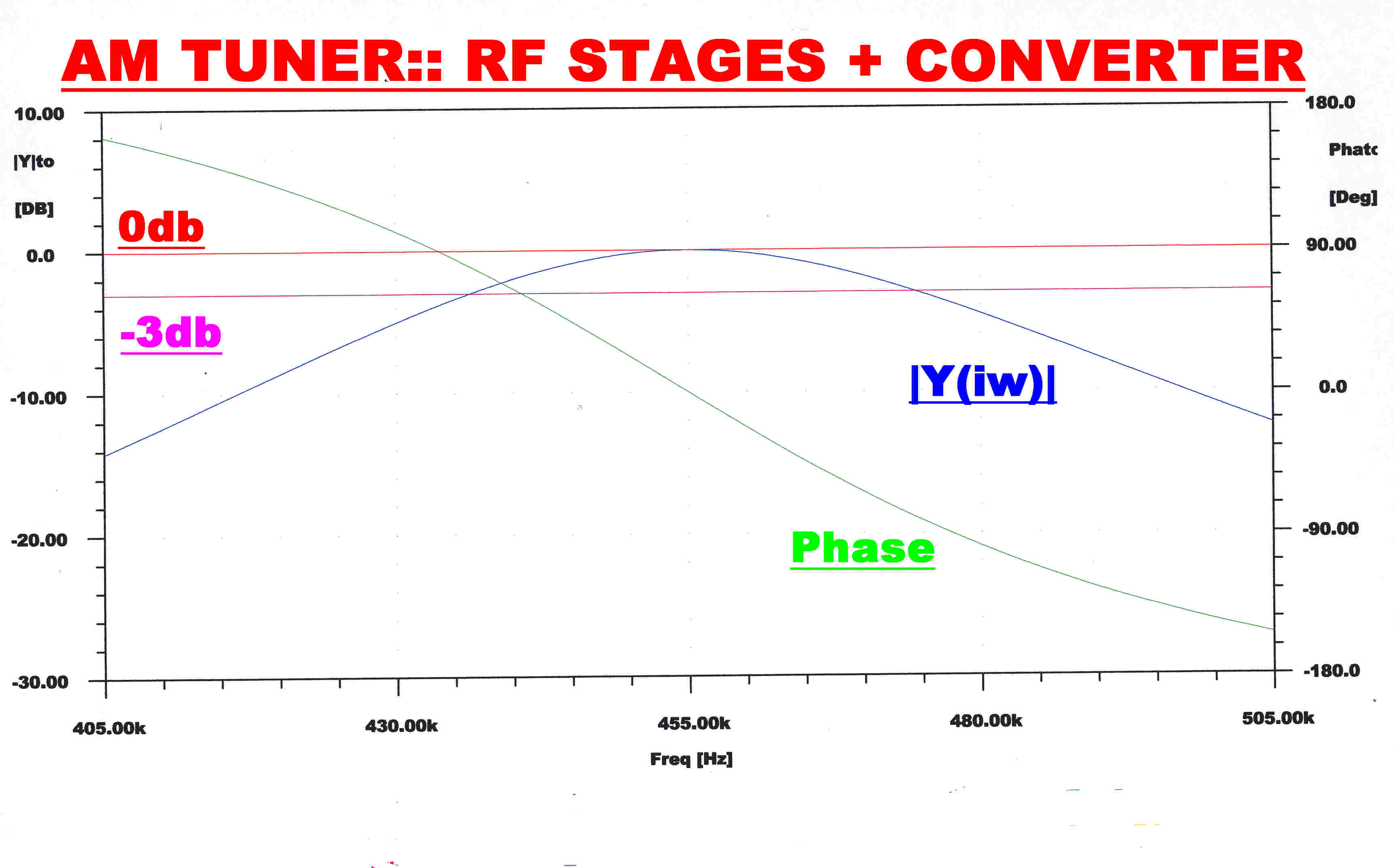
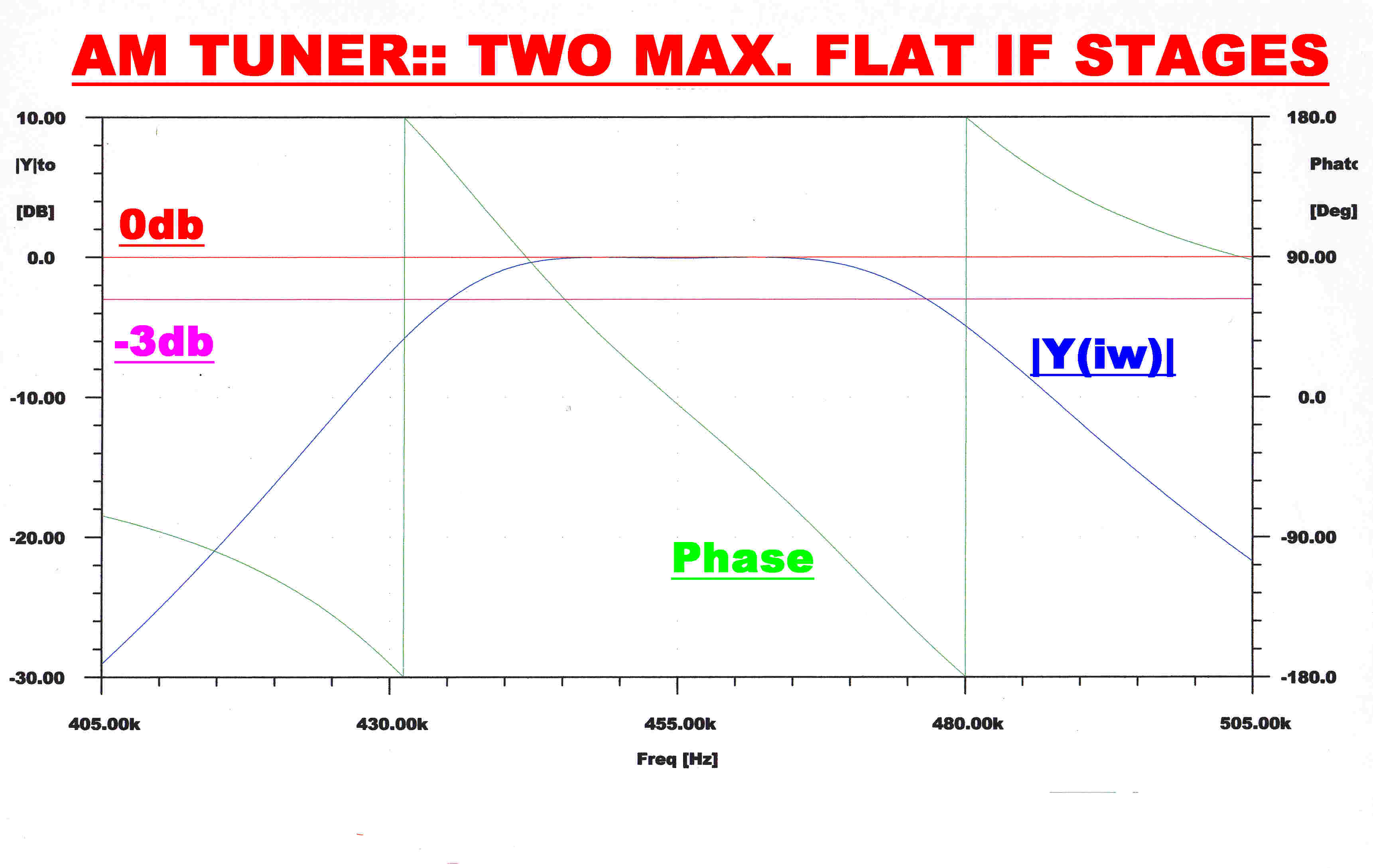
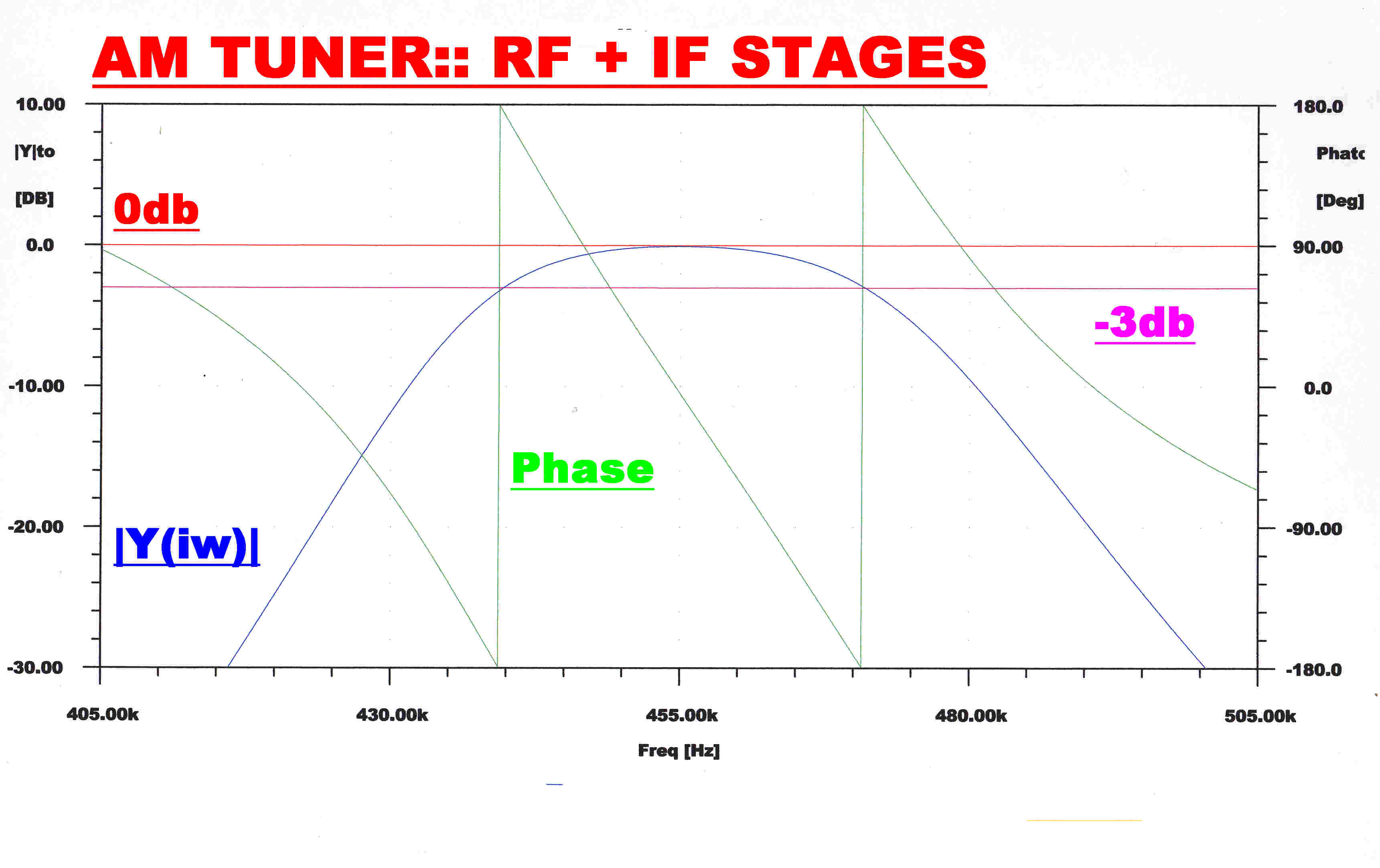
|
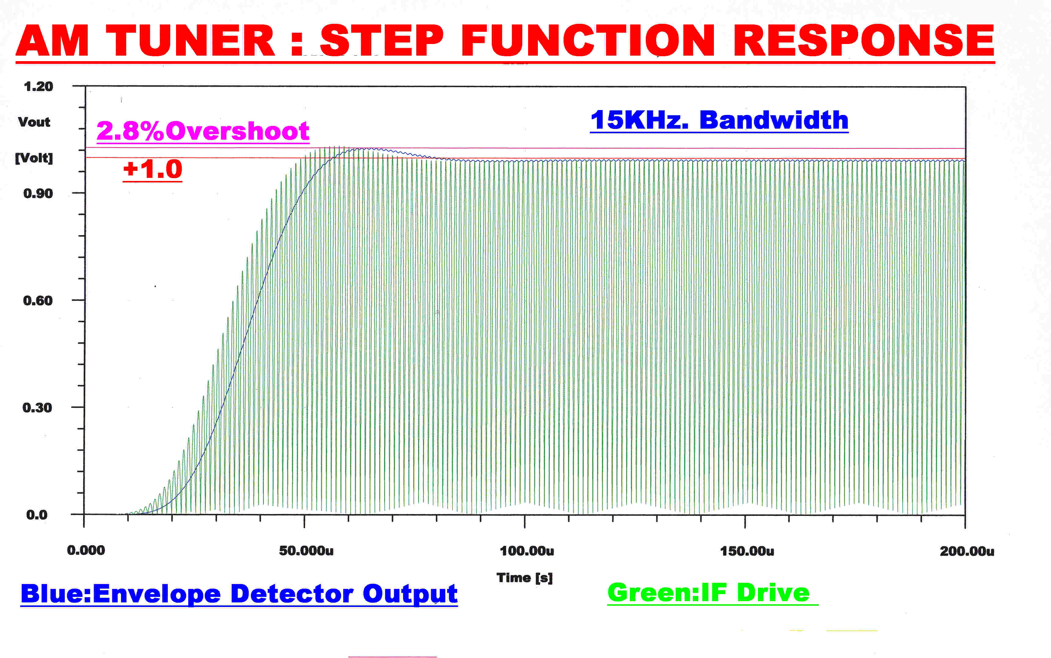
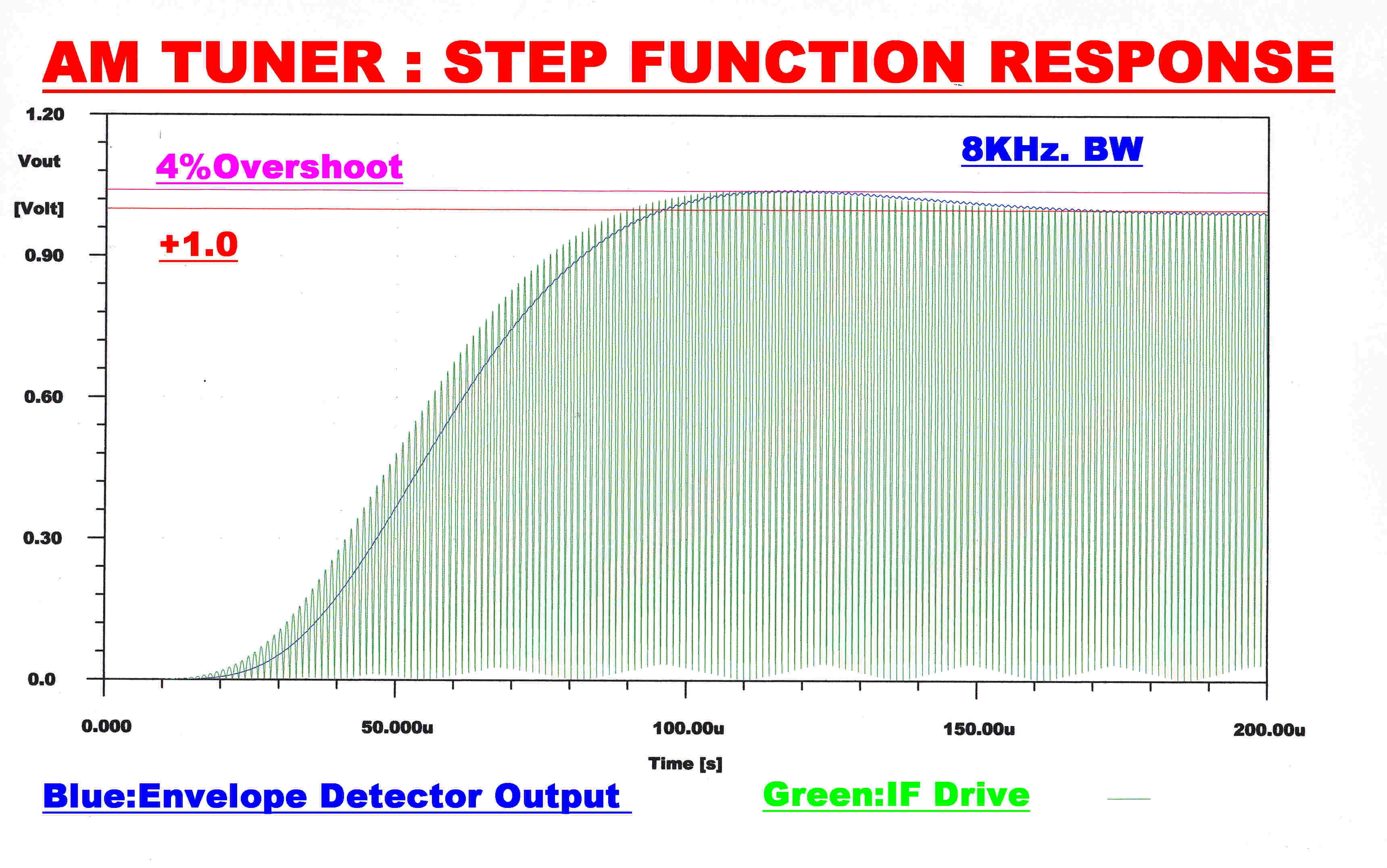
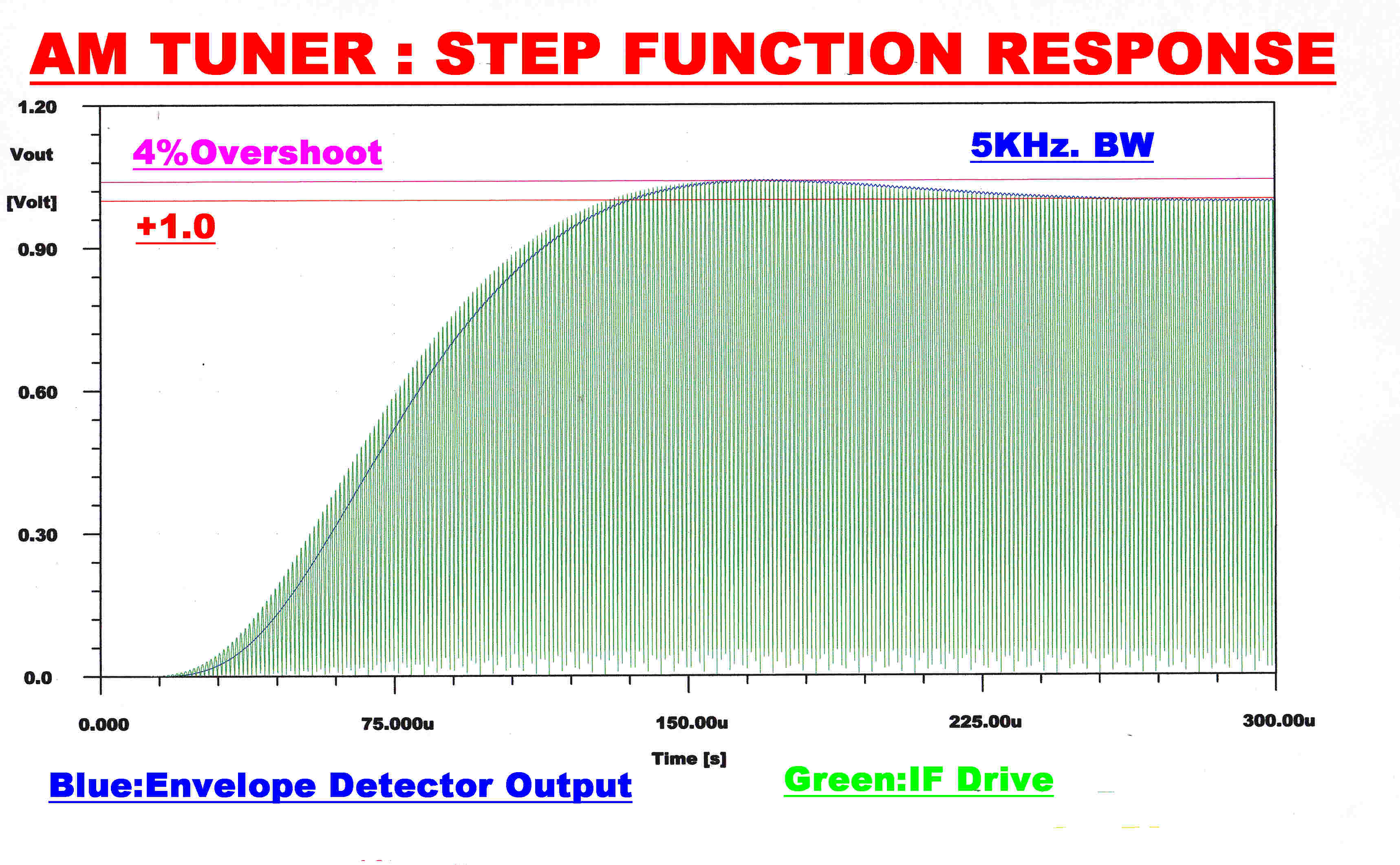
RF STAGE |
2 MAXIMALLY FLAT IF |
RF + IF |
|
|
|
|
WIDEBAND RESPONSE: 15KHz. |
RESPONSE: 8KHz. |
RESPONSE: 5KHz. |
|
|
|
Note:-The input to the envelope detector (green) gives the response of the RF + IF networks. A fourth order RC filter with a monotonic transient response filters the audio output (blue) from the envelope detector.This has little effect on the overall response which is determined by the RF and IF stages.
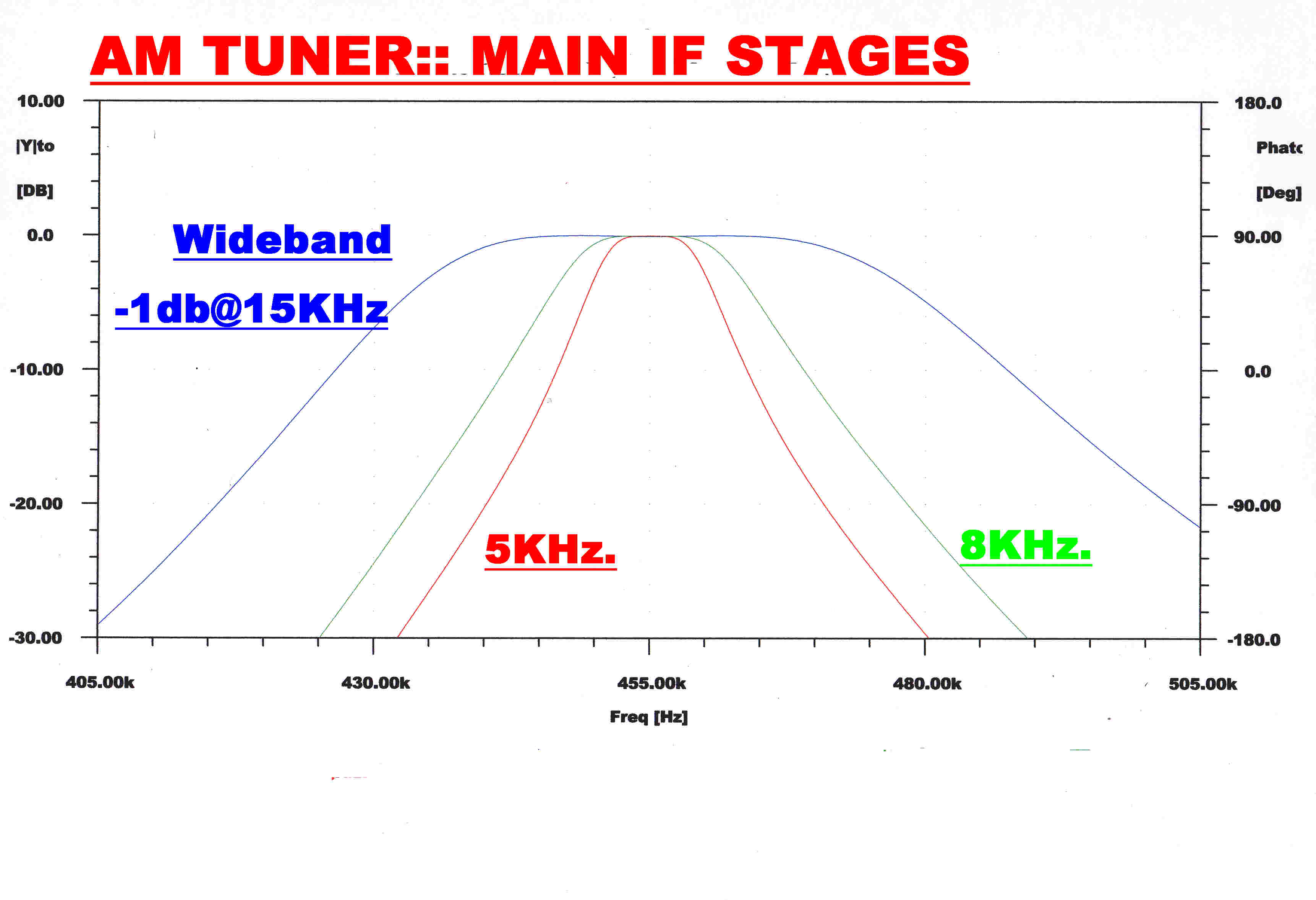 The steady state response of the IF stage for the three bandwidths position is shown on
the right.
The steady state response of the IF stage for the three bandwidths position is shown on
the right.
Note that the curves are not completely symmetrical about the centre frequency (455KHz.),
so that there is a small output from the Q demodulator, even for a perfect transmitter.
|
Plots of the steady state response of the 5th order maximally flat
and ceramic IF strips are shown on the right. |
|
|
The bandwidth of the tuner should be independent of the tuning frequency from
550KHz. to 1500KHz.
 The condition for constsnt bandwidth is now investigated:-
B = fc / 2 Q
Q = 2π fc L / R
∴ R = 4 π L B
where the tuning inductor, L, has a series resistance, R, at the carrier frequency
fc to give a modulation bandwidth of B.
Since L and B are constant, R must be constant for constant bandwidth.
Because of skin and proximity effects, R is not constant for inductors, but we
can approximate it by swamping it with an external resistance which does have a
frequency independent R.
The total tuning capacity C at 550KHz. is 510pf.
L = 1/[( 2 π fc )2 C ]
= 164.19uH.
From above:- B = 36.8KHz.
R = 75.93Ω
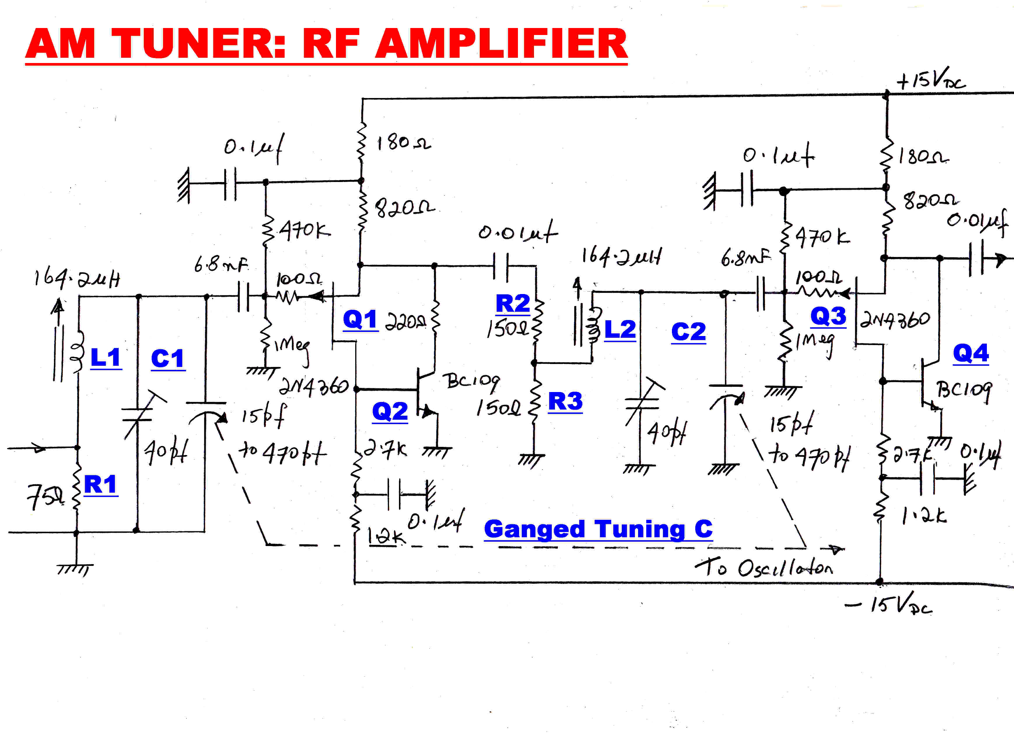
The RF amplifier circuit to realise the above conditions is shown.
Q1,Q2 and Q3,Q4 form unity gain amplifiers with a very low output impedance.
The output impedance from the divider R2, R3 is 75 ohms to give the required Q for L2.
L2's own losses increase the bandwidth a little further.
The voltage gain, A of the stage is given by:-
A = [ R3/( R2 + R3)]Q ( using Thevenin)
Q = 2πfcL ( R2 + R3 )/R2R3
A = 2π(L/R2) fc
The gain increases linearly across the band, but this is of no consequence because of the AGC.
At 550KHz. A = 37.8: at 1500KHz. A = 103.2
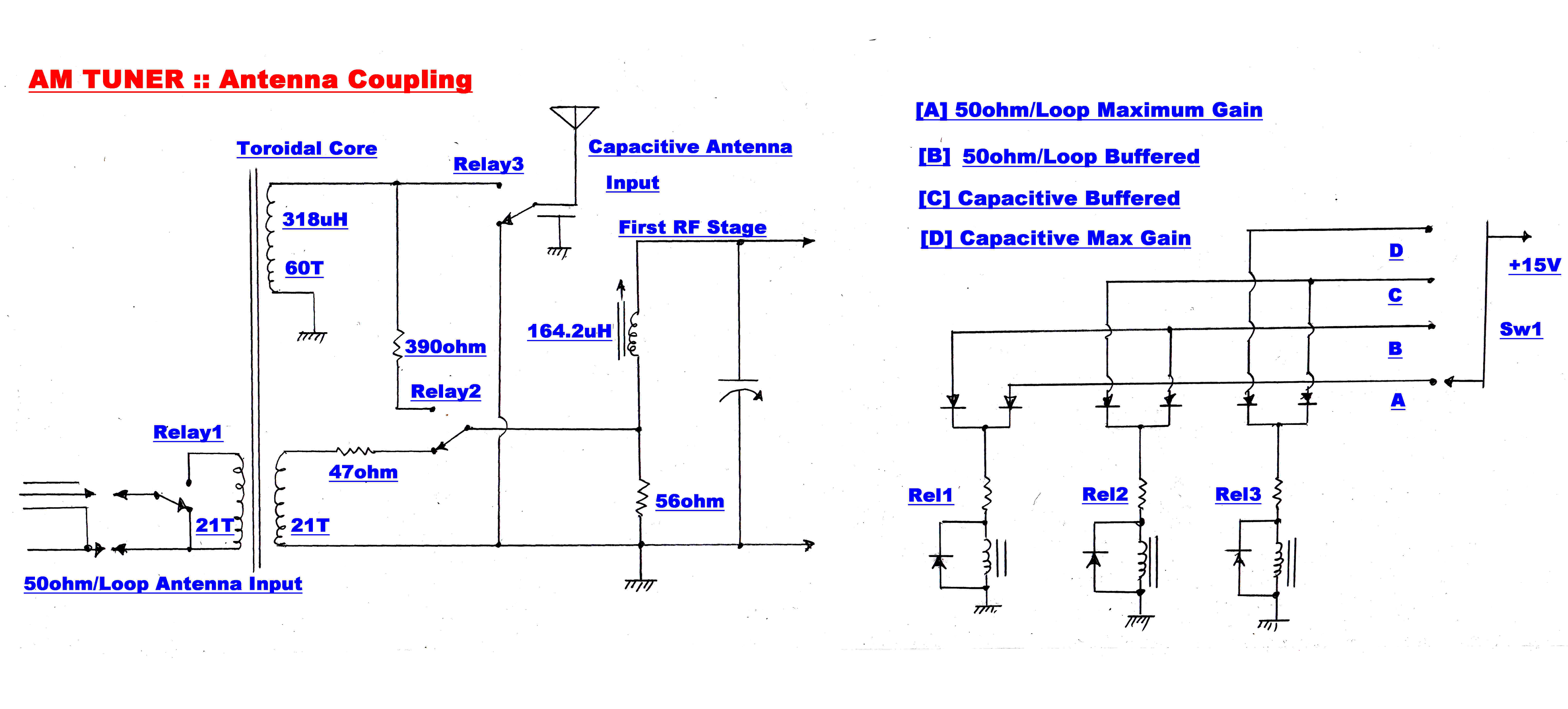 Loop or capacitive antennas present widely varying output impedances. When coupled into the
first stage RF tuned circuit this may change the centre frequency and the bandwidth.
Loop or capacitive antennas present widely varying output impedances. When coupled into the
first stage RF tuned circuit this may change the centre frequency and the bandwidth.
Both the inductive and capacitive antennas can be coupled to the first stage tuned circuit
through a resistive divider to minimise the detuning effect of the antenna.This attenuates the
input signal. Provision for more direct coupling is also provided for low signal strengths.
The antenna coupling network is shown on the right.
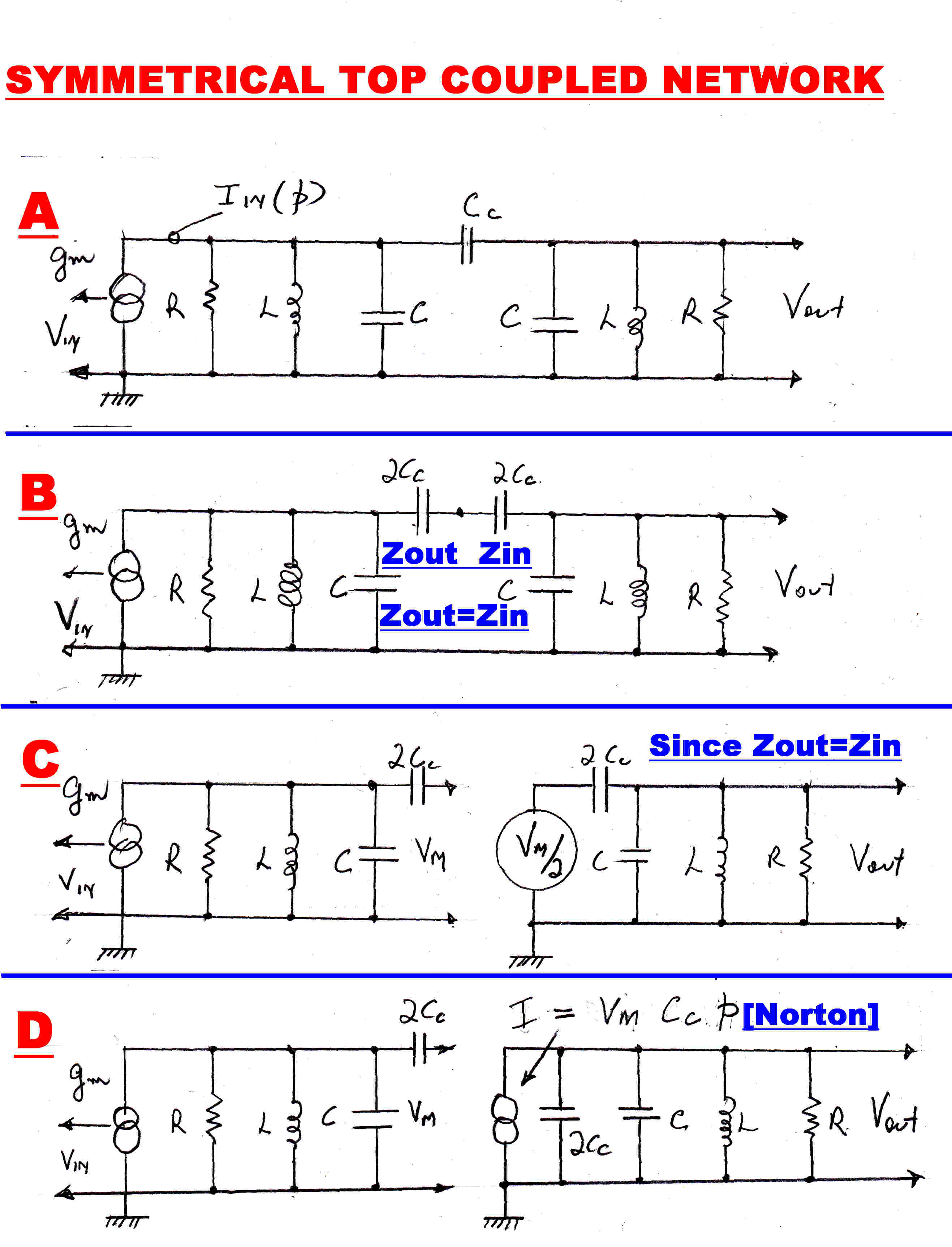 The circuit of second order top coupled network is given in (A)
The transfer inpedance of any unloaded four terminal network with internal
symmetry is given by:-
Zt = -y12/[ y112 - y122 ]
A better feel for the network can be had by adopting a more heuristic analysis.
Suppose the network is split into two symmetrical sections as in (B).
The output impedance of the left hand side is equal to the input impedance of
the right hand side. If the network is broken, then the open circuit voltage on the left hand side
drops to one half when the right hand side is connected.
We can work out the transfer impedance of the left and right hand side independently and then join
them together, knowing the voltage on the common node will drop by one half.
Referring to (C):-
The transfer impedance Zt of the LHS is given by:-
Zt(p) = Vm(p)/Iin(p) = Lp/[ 1 + (L/R)p + LCp2 ]
When connected, the voltage driving the RHS is Vm/2 as shown in (C).
This voltage generator can be transformed by Norton to the current generator shown in (D).
For the RHS we can the write:-
Vout(p) = I(p) Lp/[ 1 + (L/R)p + L( C + 2Cc)p2 ]
But I(p) = ( Vm/2 )( 2 Cc p ) = VmCc p
∴ Zt(p) = Vout(p)/Iin(p)
= [ CcL2p3] / [ 1 + (L/R)p + L( C + 2Cc)p2]
[ 1 + (L/R)p + LCp2 ]
This transfer impedance has:-
(a) Three zeros at the origin.
(b) Two poles:-
pH = σ +iωH
= -1/(2RC) ± i [ 1/(LC) - 1/(4R2C2)]1/2
pL = σ +iωL
= -1/(2RC) ± i [ 1/(L(C + Cc ) - 1/(4R2C2)]1/2
Equating:-
σ = -1/(2RC)
ωH = [ 1/(LC) - σ2 ]1/2
ωL = [ 1/(LC + 2 Cc) - σ2 ]1/2
Now C; σ; ωH and ωL are given, solving for R, L,
C and Cc we get:-
R = -1/( 2 σ C )
L = 1/[ C( ωH2 + σ2 ) ]
Cc = (1/2)[ 1/( L( ωL2 + σ2) ) - C ]
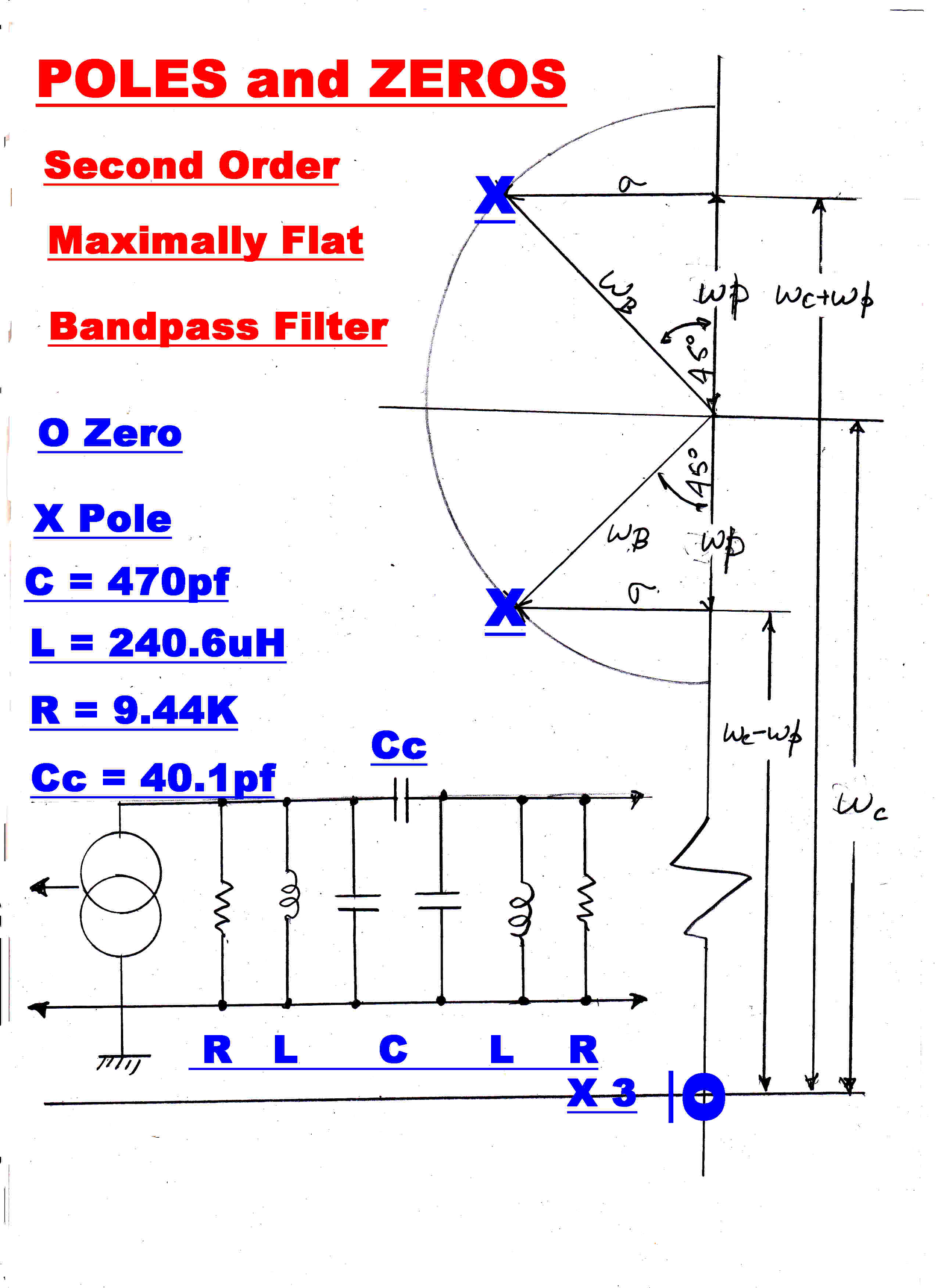
The narrow band approximation for second order maximally flat poles is shown opposite
so that:-
σ = ωB sin(45)
ωH = ωc + ωB cos(45)
ωL = ωc - ωB cos(45)
It was shown above that the required bandwidth is 25.38KHz. Using the above equations,
the values for the network are shown.
The above analysis suggests a method of alignment.
The tuned circuit L-C resonates at a frequency of the upper pole fc
+ fp. Adding 2Cc in parallel brings the resonant frequency
down to that of the lower pole fc - fp. If the output is shorted,
the input L-C is shunted by Cc, so that the resonant frequency is fc.
If the shunt is replaced by a resistor of low value, the voltage across it gives an indication
of resonance without circuit loading by a measuring probe.
The alignment procedure:-
(a) Provide a removable link directly after Cc.
Break this link and set Cc to the calculated value.
(b) Shunt the output with a low value resistor and tune the LHS L-C for a maximum at
the carrier frequency fc.
(c) Shunt the LHS and tune the RHS for a maximum.
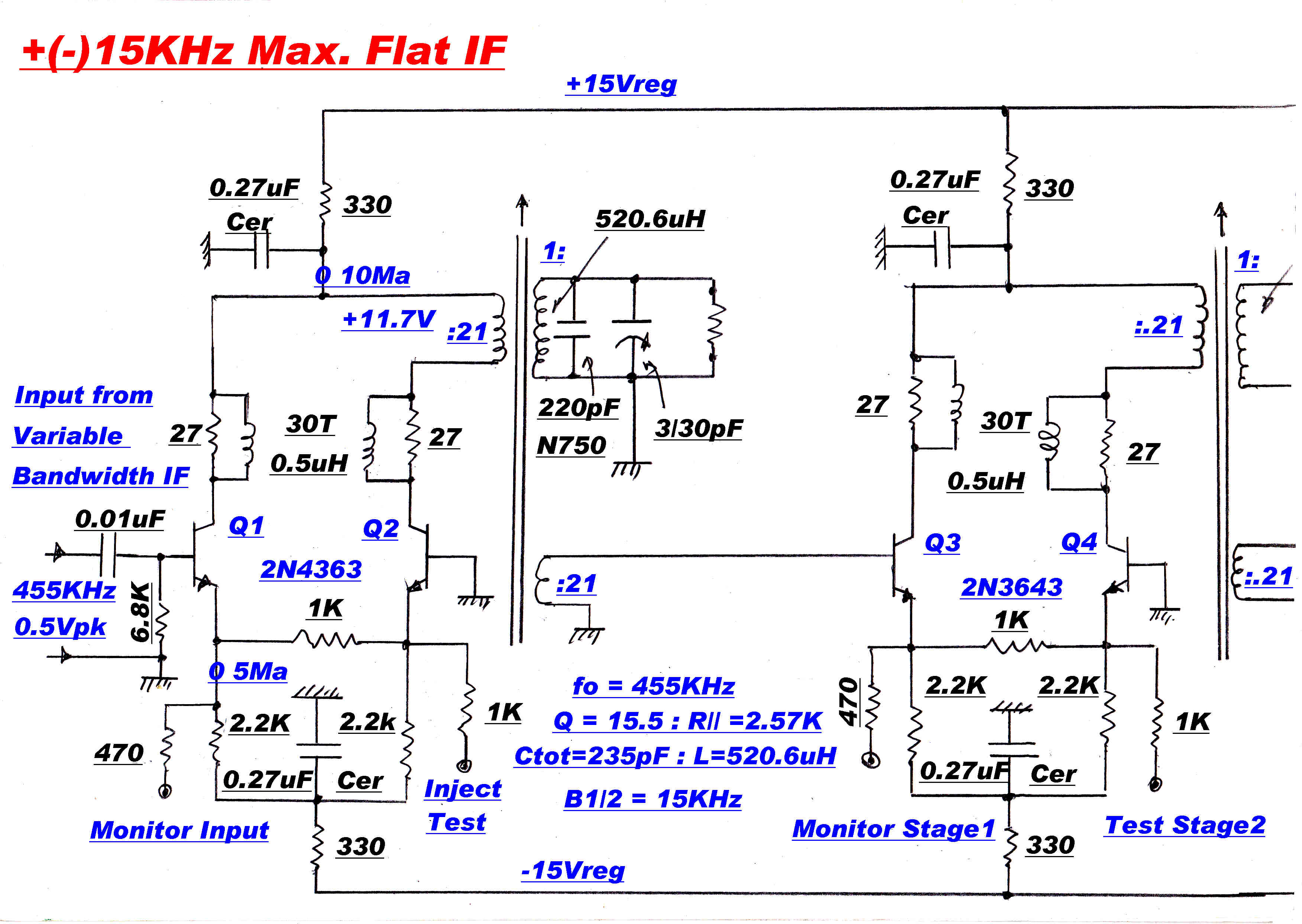
 A ± 15KHz. bandwidth maximally flat IF can be cascaded with the wide band IF to provide
extra selectivity.
A ± 15KHz. bandwidth maximally flat IF can be cascaded with the wide band IF to provide
extra selectivity.
The poles of a 5th order bandpass maximally flat transfer function are shown on the right.
Each pole is realised by a single tuned circuit.
The transfer impedance is given by:-
z(p) = Lp/[ 1 + (L/R)p + LCp2 ]
This has poles at:-
-1/(2RC) ±i[ 1/(LC) - 1/( 2RC)2 ]
Put s = 1/(2RC) and
ω = [ 1/(LC) - s2 ]1/2
C is given, so that:-
R = 1/(2sC)
L = 1/[ Cω2( 1 + (s/ω)2 ) ]
Q = R/( ωL) so that:-
Q = [ω/(2s)][ 1 + (s/ω)2 ]
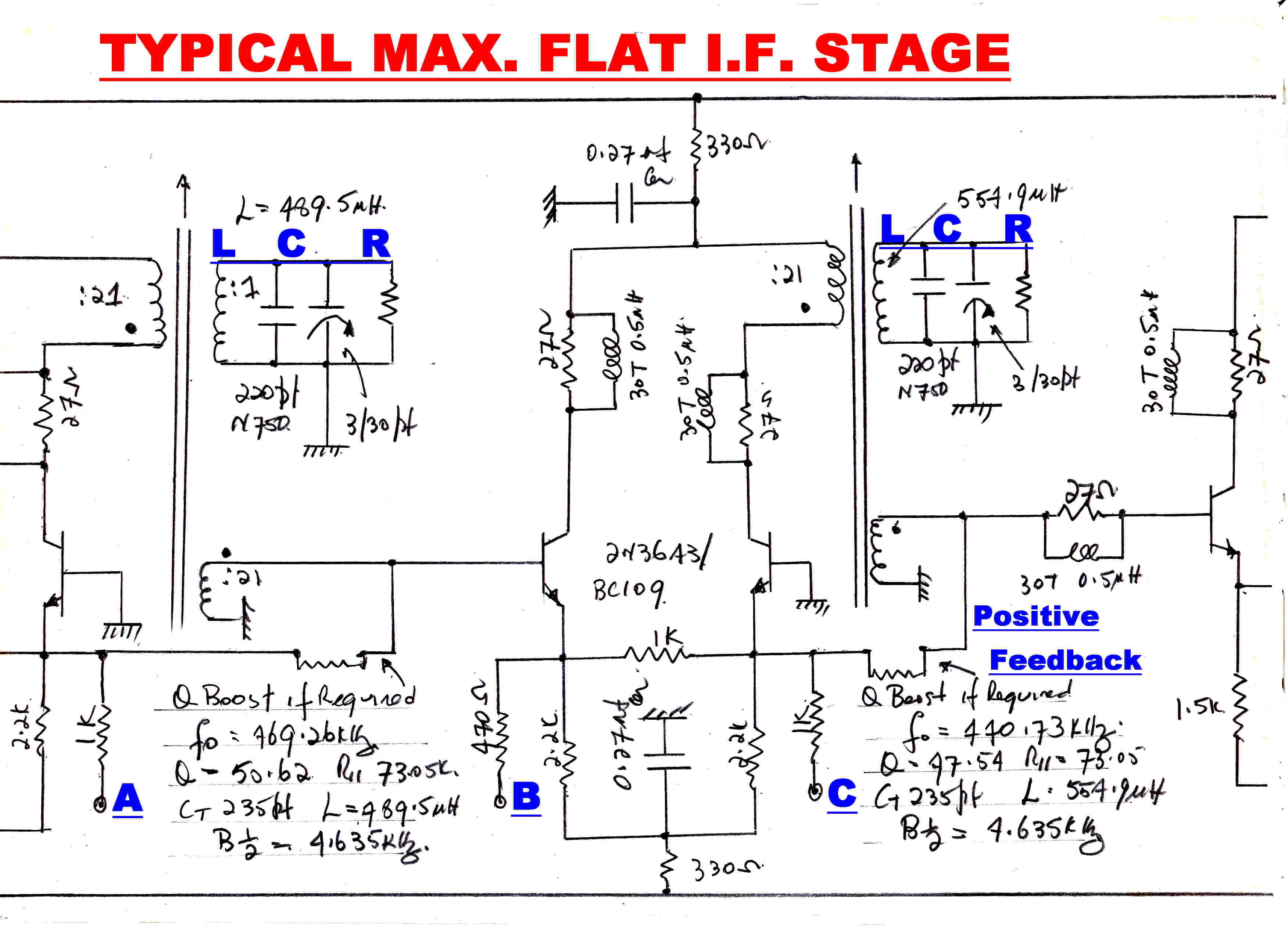 A typical maximally flat IF stage is shown on the right.
Provision is made to adjust the resonant frequency and bandwidth of each individual
tuned circuit. Test signals are injected at points such as A and C. The response of the previous
stage can be monitored at points such as B.
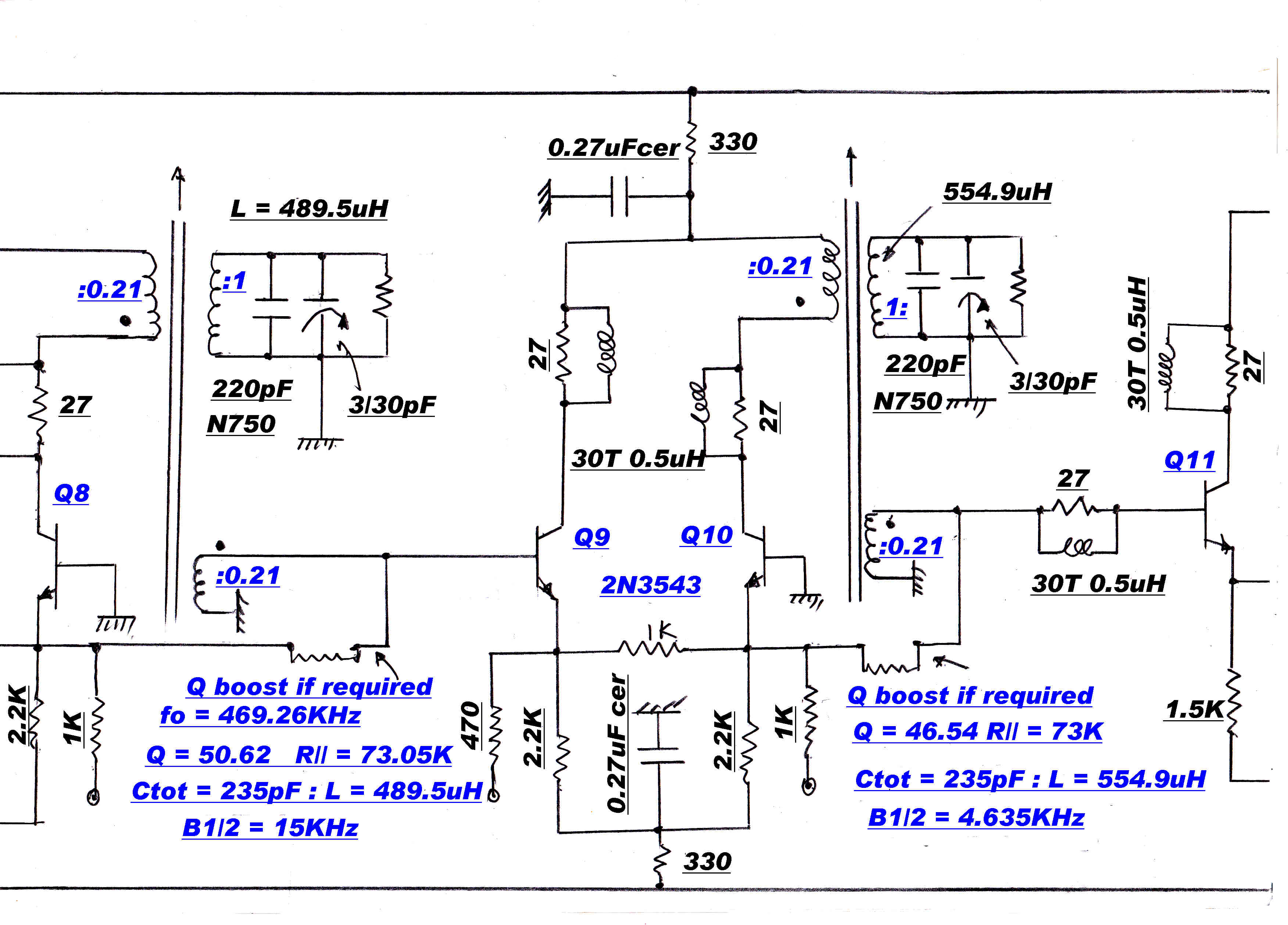
In stages which require a Q higher than the Q of the inductor, positive feedback can be introduced
to provide a negative parallel resistance.
Details of the coupling networks.
Nominal tuning C of all networks = 235pf.
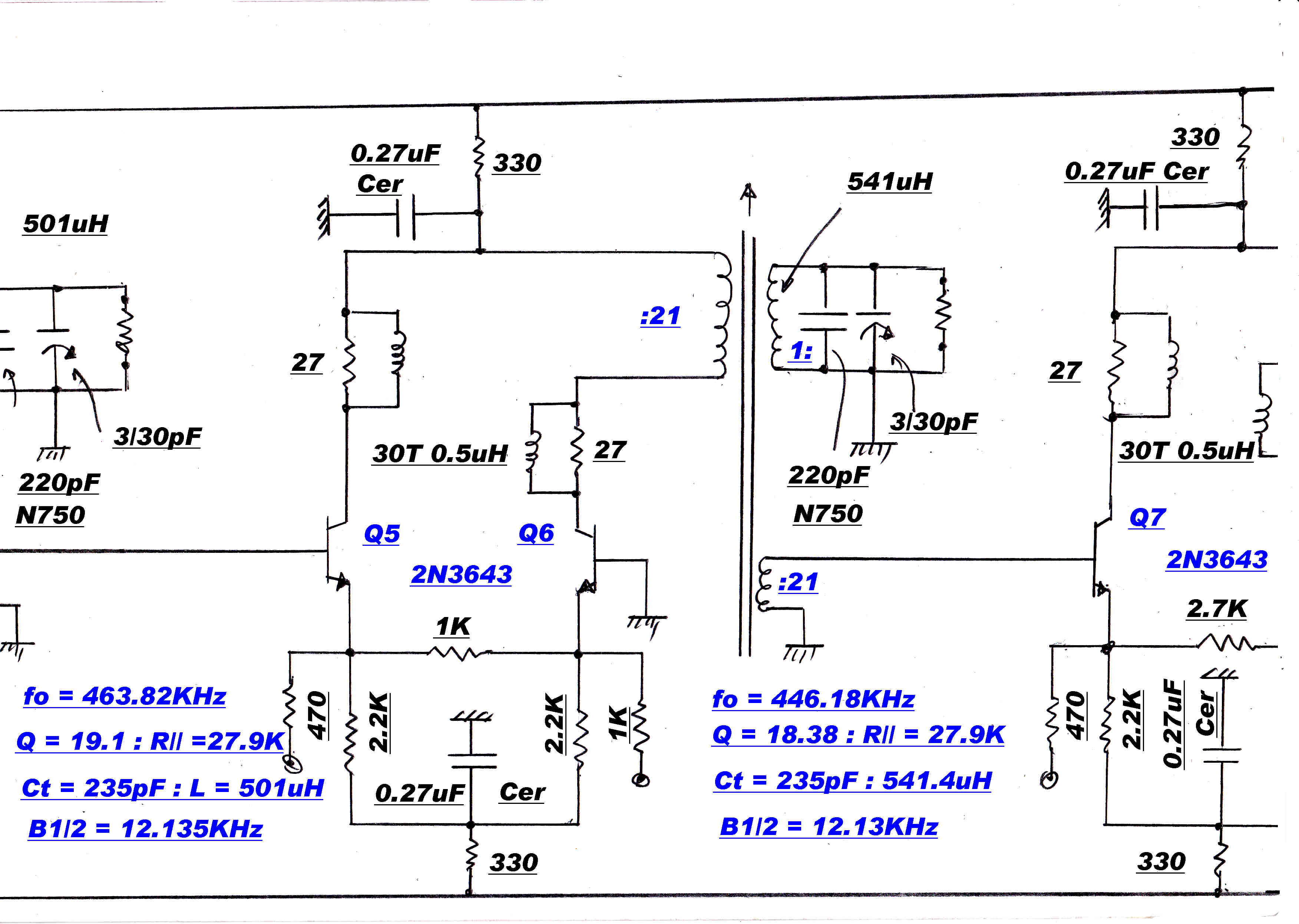
Stage 1:- fo= 455.0 KHz: B1/2=15KHz: L=520.6uH;Q=15.5:R//tot=22.5K
Stage 1:- fo= 463.8 KHz: B1/2=12.14KHz: L=501uH;Q=19.1:R//tot=27.9K
Stage 1:- fo= 446.2 KHz: B1/2=12.14: L=541.4uH;Q=18.4:R//tot=27.9K
Stage 1:- fo= 469.3 KHz: B1/2=4.635KHz: L=489.5uH;Q=50.6:R//tot=73.1K
Stage 1:- fo= 440.7 KHz: B1/2=4.635KHz: L=554.9uH;Q=50.6:R//tot=73.1K
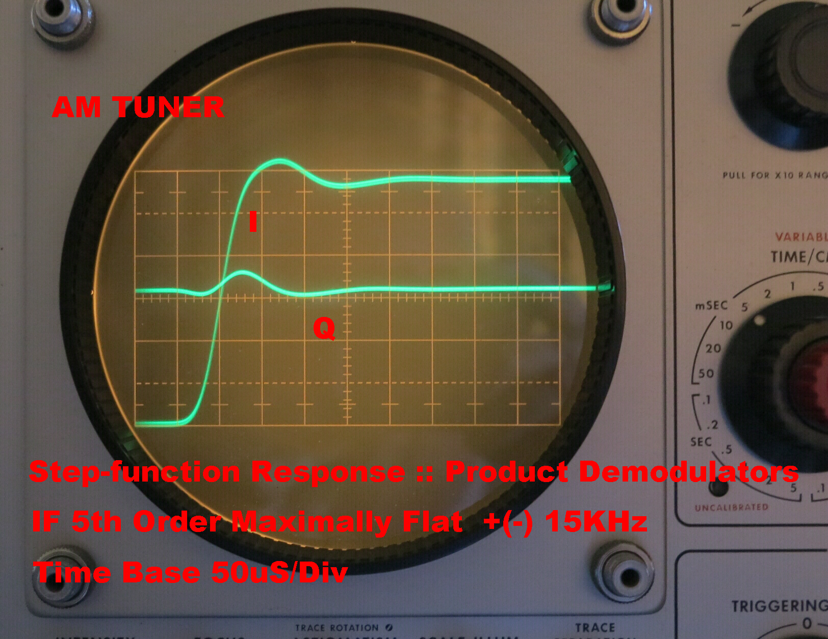 The steady state response of the Max. Flat filter standing alone is shown on the right.
The overall step function response of the receiver with the max. flat filter in circuit is also shown.
This is heavily modified by the post detection filters after the product detectors.
The steady state response of the Max. Flat filter standing alone is shown on the right.
The overall step function response of the receiver with the max. flat filter in circuit is also shown.
This is heavily modified by the post detection filters after the product detectors.
Note that the quadrature component has increased due to the asymmetry in the pass band.
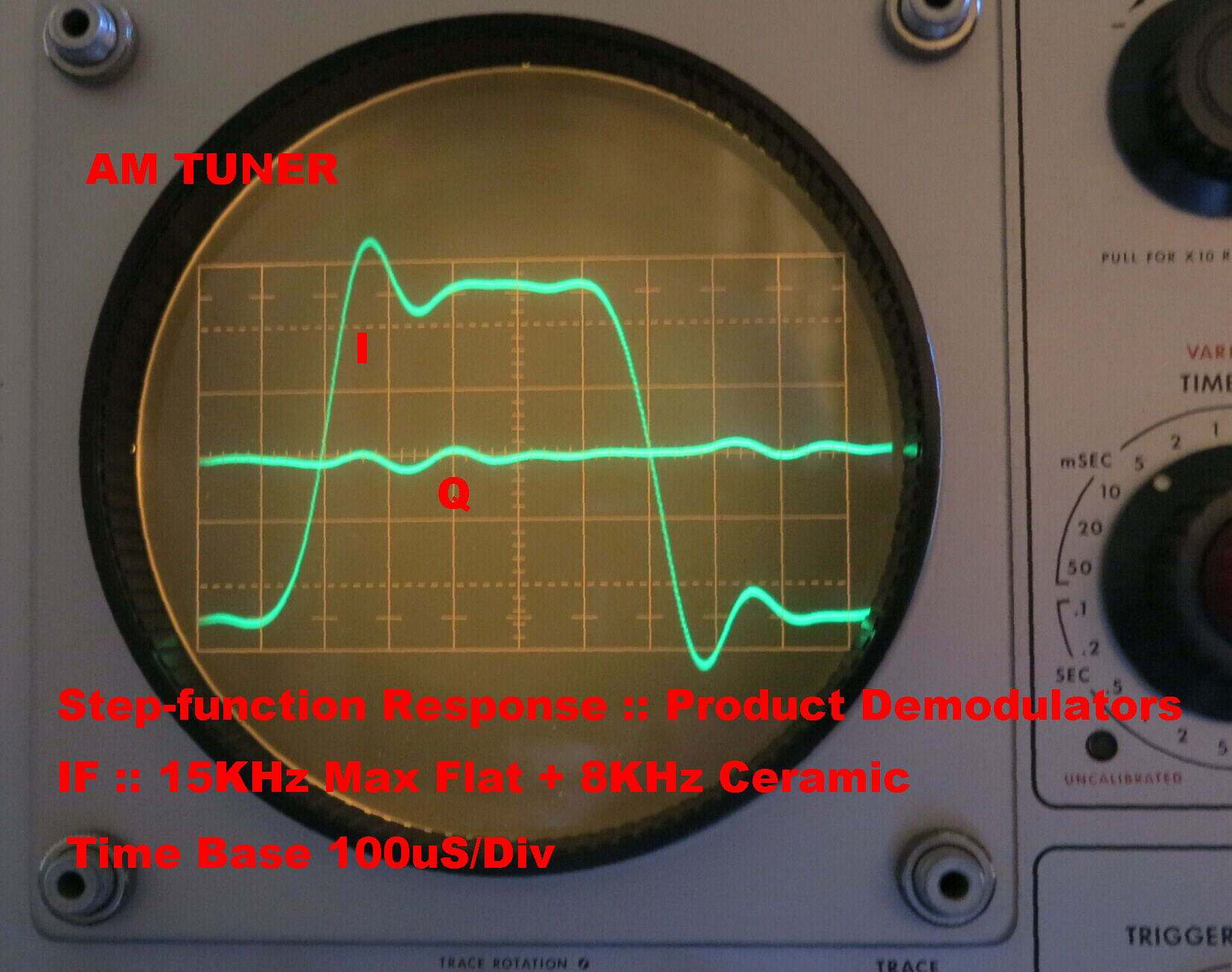 The steady state response of the Ceramic filter standing alone is shown on the right.
The overall square wave response of the receiver with the max. flat filter and the ceramic filter
in circuit is also shown.
The steady state response of the Ceramic filter standing alone is shown on the right.
The overall square wave response of the receiver with the max. flat filter and the ceramic filter
in circuit is also shown.
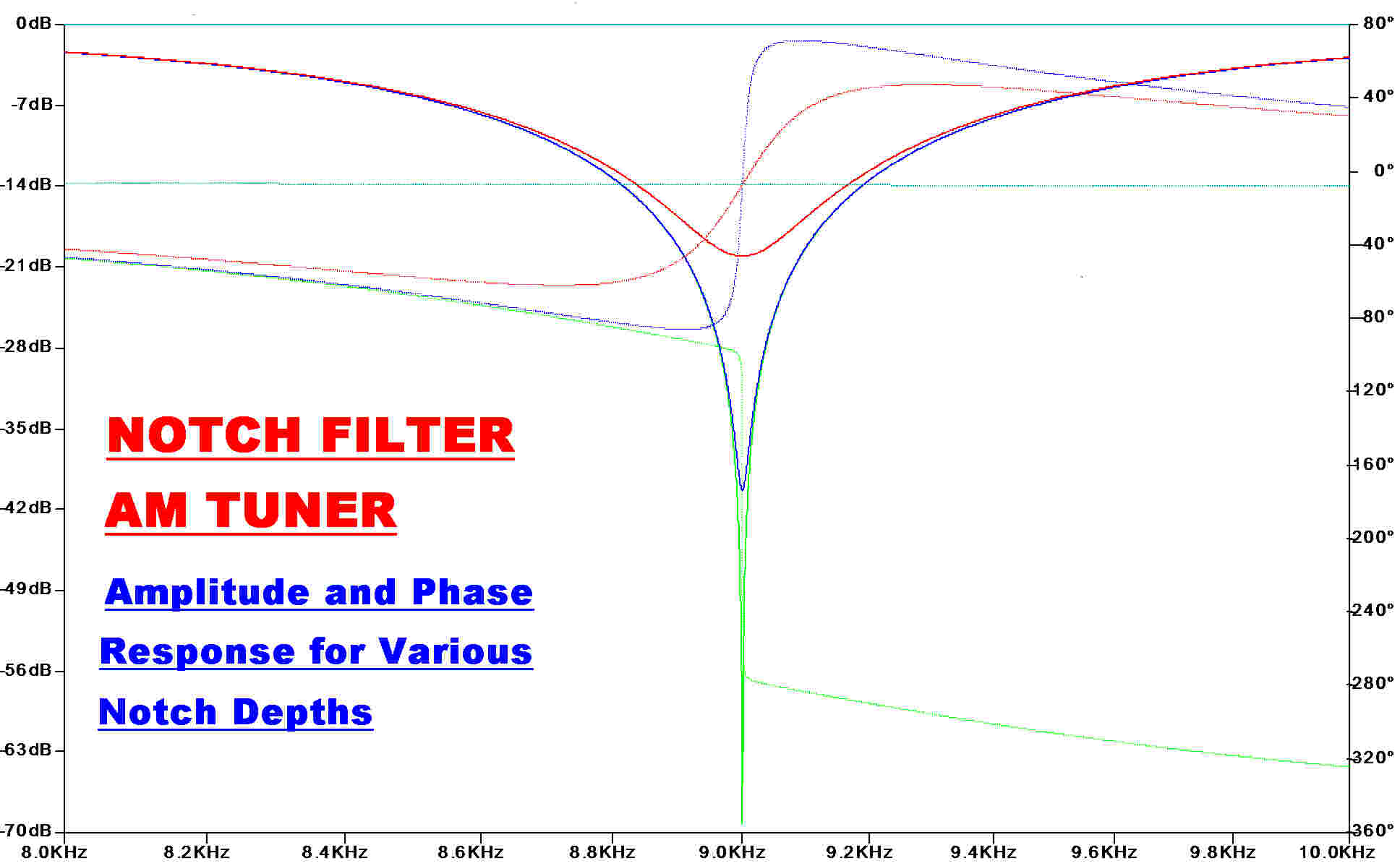
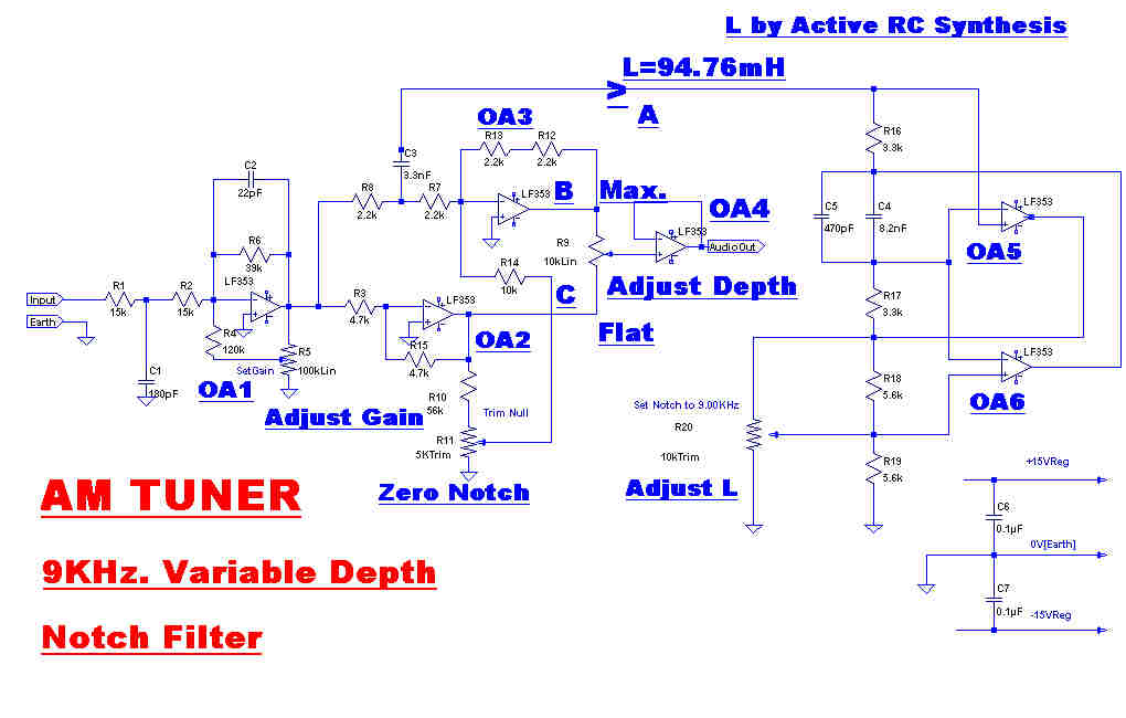 The circuit and response of the variable depth 9KHz. notch filter are shown to the right.
OPAmps OA5 and OA6 generate an inductance, L, looking into point A.
The nominal value of this inductance is 94.76mH, but this can be trimmed with the potentiometer R20
to adjust the resonant frequency to 9KHz.
L forms a series resonant circuit with C3 (3.3nF). The series resistance is given by R7 and R8 in
parallel(1.1K).
At the resonant frequency L and C3 have near zero impedance, so that the junction of R7 and R8 is
close to earth potential, giving deep rejection on the output of OA3.
OA5 and OA6 are not perfect op. amps, so L has a small resistive component. The voltage developed
across this is cancelled by a small out of phase voltage develped across R11. This can be adjusted to
give a very deep null on the output of OA3.
The output on OA2 is flat, so the voltage on the potentiometer, R9, goes from flat to deep null.
The amplitude and phase response is plotted for various positions of R9.
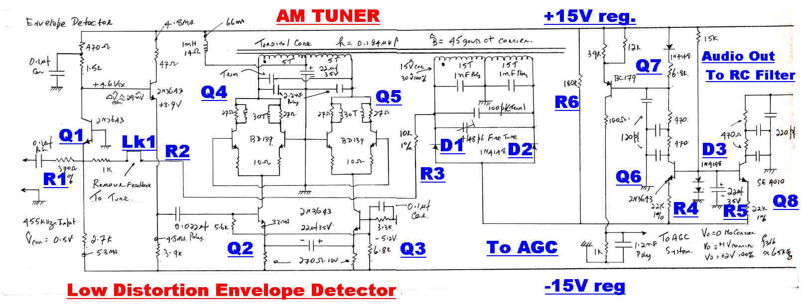
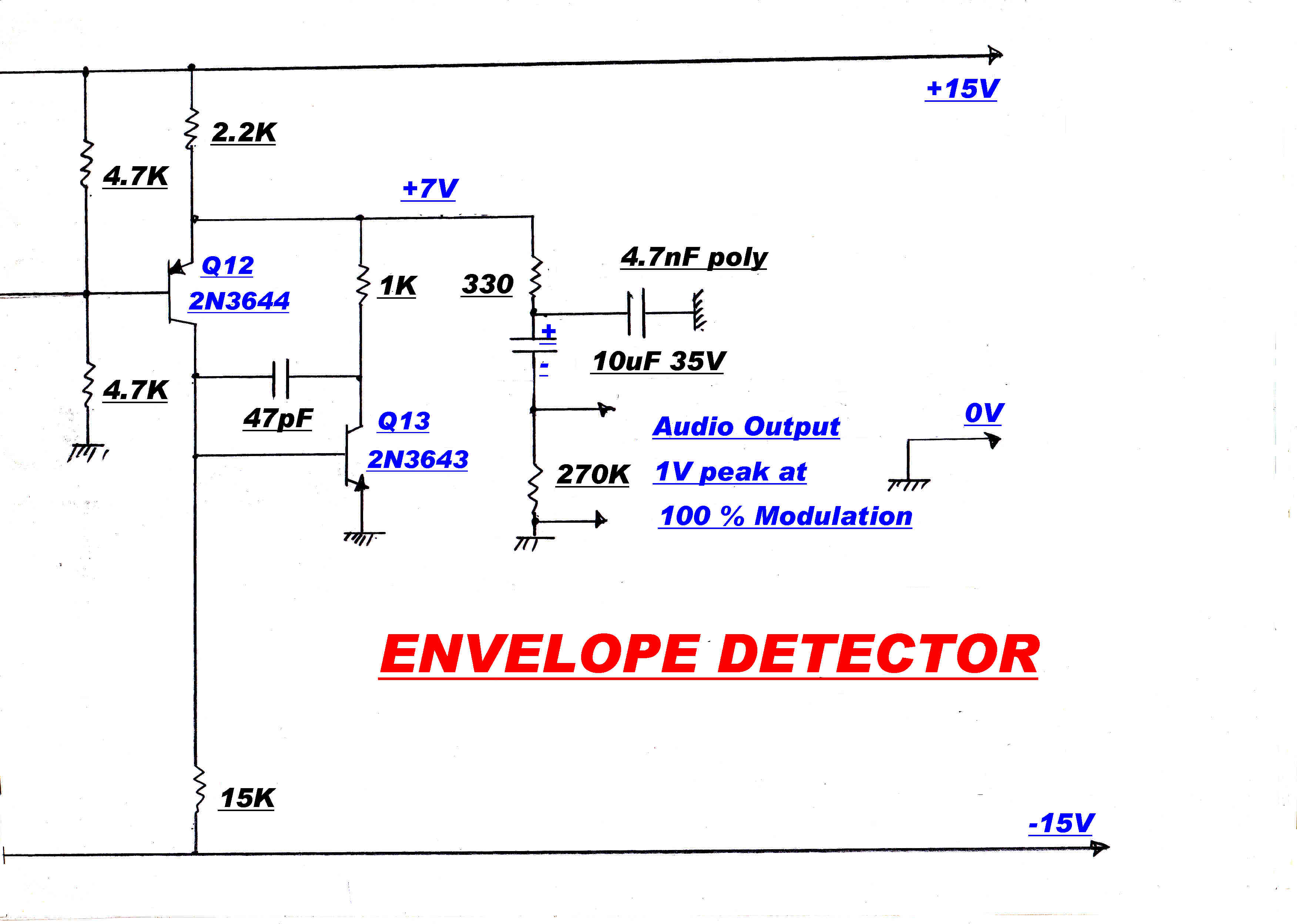
A truncated circuit of the envelope detector is shown above.
AM demodulation by a full wave rectifier with a resistive load is attractive for the following reasons:-
(a) The output ripple is at twice the IF frequency and frees up the design of the post
detection filter.
(b) The demodulated output applied to the post detection filter is free from transient errors.
Distortion is introduced by the non-linear relationship between the diode current and voltage.
This can be reduced in three ways:-
(1) The rectifier can be driven from a high voltage, so that the diode drop and any non-linearity
in it becomes insignificant.
(2) A constant current generator can be used as the load. The rectifier then presents a non-linear
load to the driving amplifier.
(3) The non-linearity can be eliminated by using the same diode load combination as the feedback
network in an operational amplifier. This demands very good transient performance in
the operational amplifier.
The first technique is adopted because of its simplicity.
15 volts peak is applied to the
rectifier at carrier.
The diode drop is compensated by the double diode D3 and the input offset of
transistors Q6 and Q8. A small bias current of 40uamps is applied to each diode by R6.
The detector will track the carrier down to zero input volts.
The diode rectifier is driven by an amplifier with heavy feedback [ >500 ] through the resistive
chain R2/R3. The LC circuit in the collectors of Q4/Q5 has a bandwidth of 5KHz. and forms
the stabilising pole in the feedback loop. The feedback loop can be broken at the link Lk1 to
enable tuning of the LC network to 455KHz.
A DC coupled output drives the AGC and modulation meters.
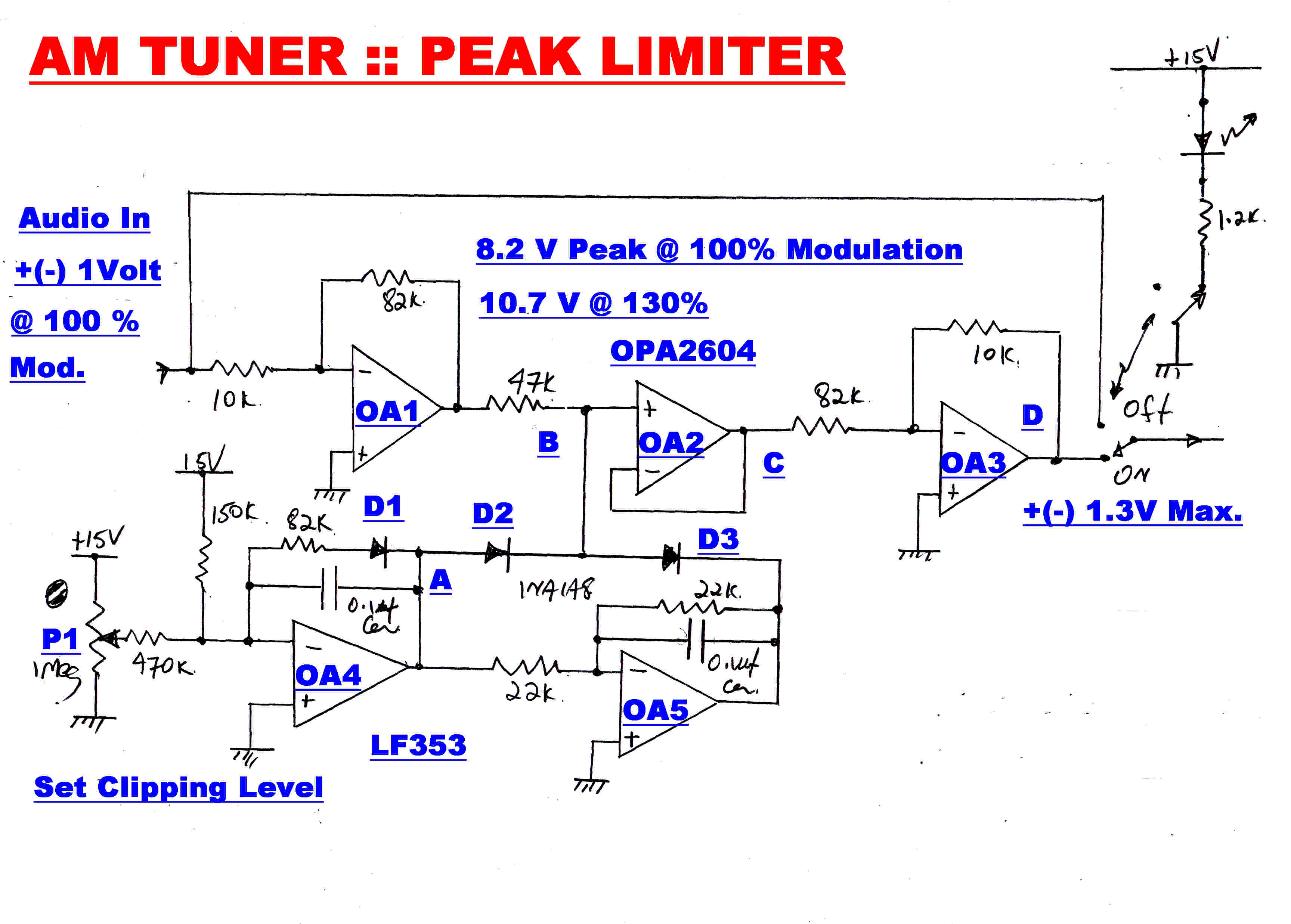
The tuner is intended for a high quality service on ground wave, but provision is made
for noisy signals which also may have suffefred from multipath transmission.
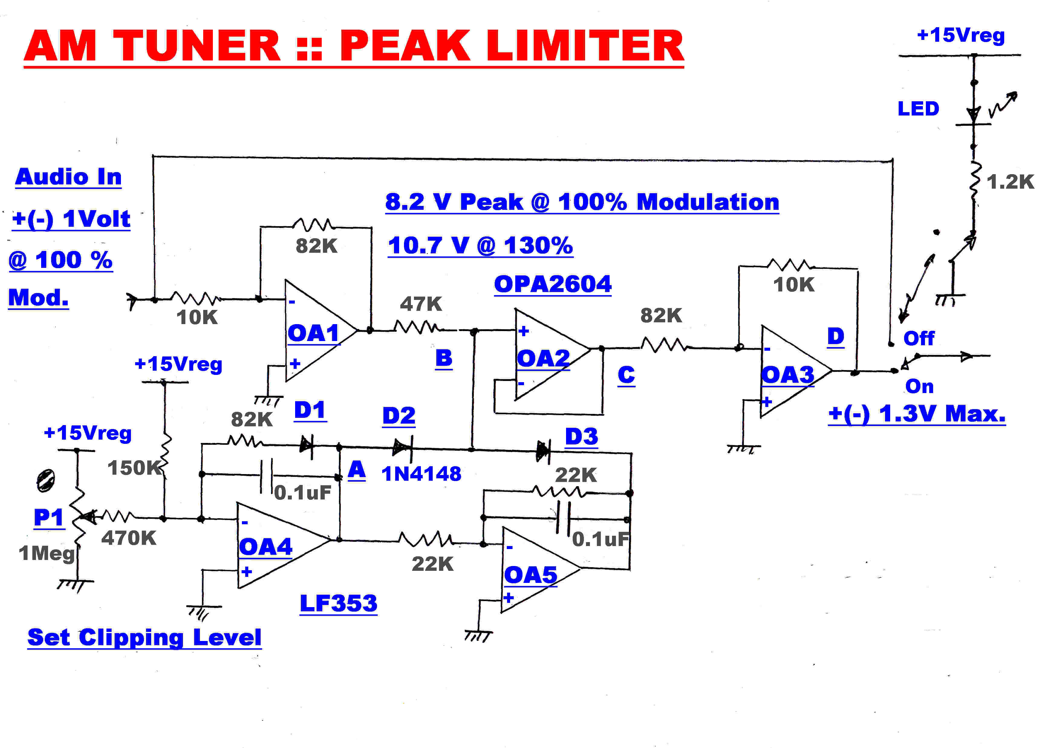
A peak limiter can be switched into circuit to limit the peaks from impulsive noise to 130%
of carrier level. The impulsive noise on the output of an envelope detector can only increase in
the direction of positive modulation. With a product drmodulator the noise is bidirectional,
so the limiter must also limit positive and negative audio peaks.
The signal level is increased by a factor of 8.2 in OA1 to give a sharper limit level.
The limit reference voltage is generated in OA4.
Diode D1 compensates for the thermal drift in the limit diodes D2 and D3.
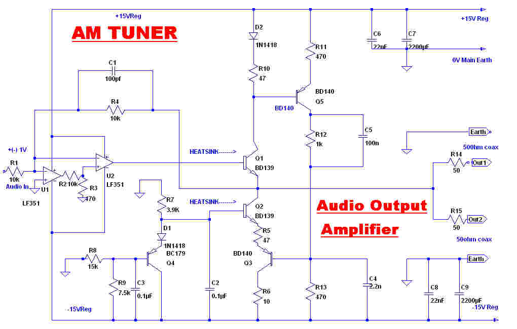 The audio output amplifier is designed to drive two unterminated 50 ohm coax. cables
with extremely low non-linear and transient distortion. Long unterminated cables present a
high capacity load to the output. The output stage is designed to handle these loads.
The audio output amplifier is designed to drive two unterminated 50 ohm coax. cables
with extremely low non-linear and transient distortion. Long unterminated cables present a
high capacity load to the output. The output stage is designed to handle these loads.
Cascaded opamps. U1 and U2 provide a very high gain in the forward loop over the audio band.
This reduces non-linear distortion to a vanishingly small value.
The high frequency open loop transfer function is determined by U2.
The frequency and transient response is determined by R1 and C1, and so the 3db point is 159KHz.
The collector current of the output transistor Q1 is sensed by R10 and D2.
Q2-Q3-Q5 form a DC coupled unity gain amplifier. If the collector current of Q1 changes by
ΔI, then the collector current of Q2 changes by -ΔI, so that the current change at
the output terminal is 2ΔI.
The quiescent current in the output stage is set by the divider R8-R9 to about 50MA.
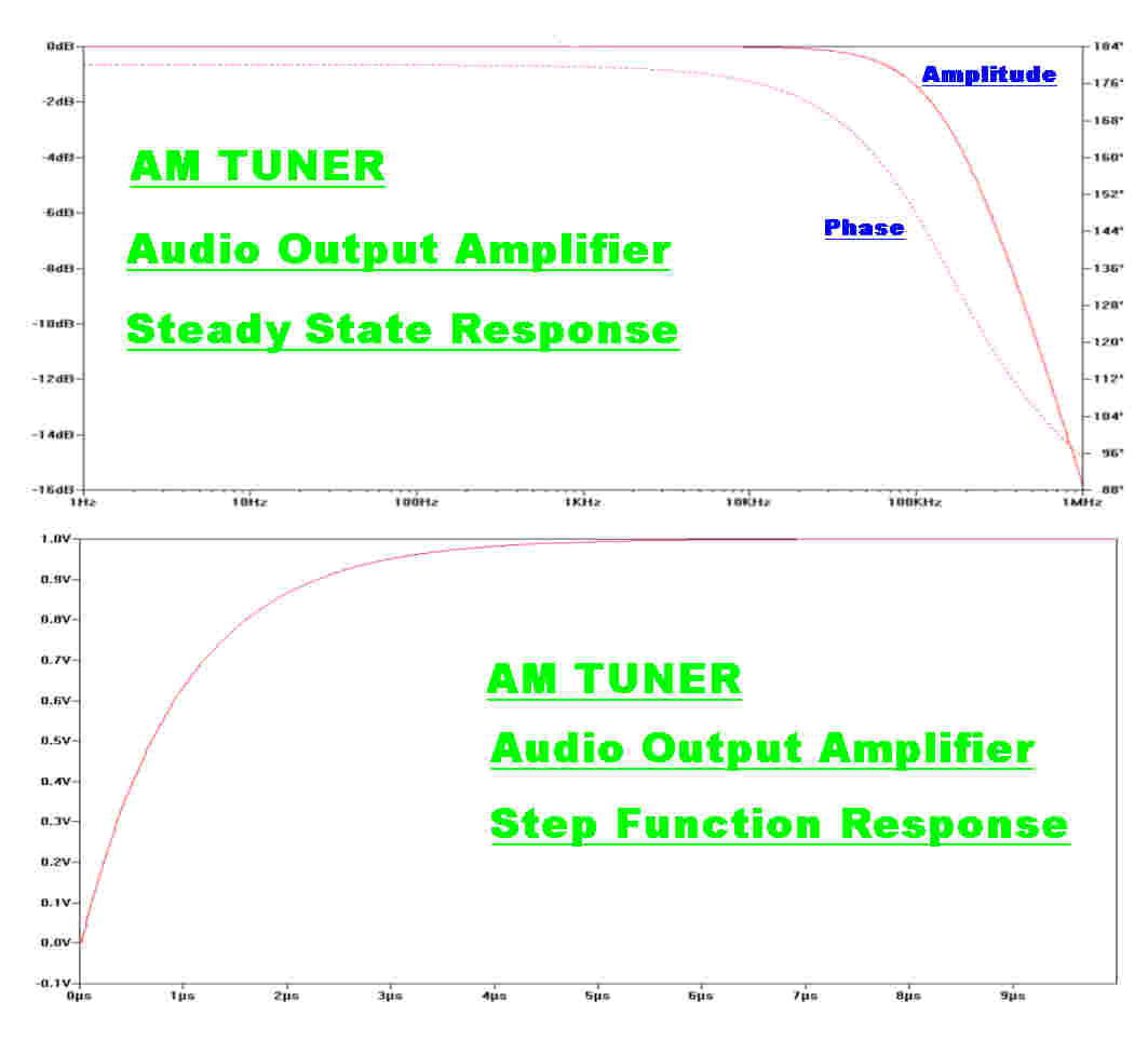 The steady state and transient responses of the amplifier are shown opposite.
The amplifier is flat and approximately phase linear over the complete bandwidth of
the tuner, so it will have no significant effect on the overall response.
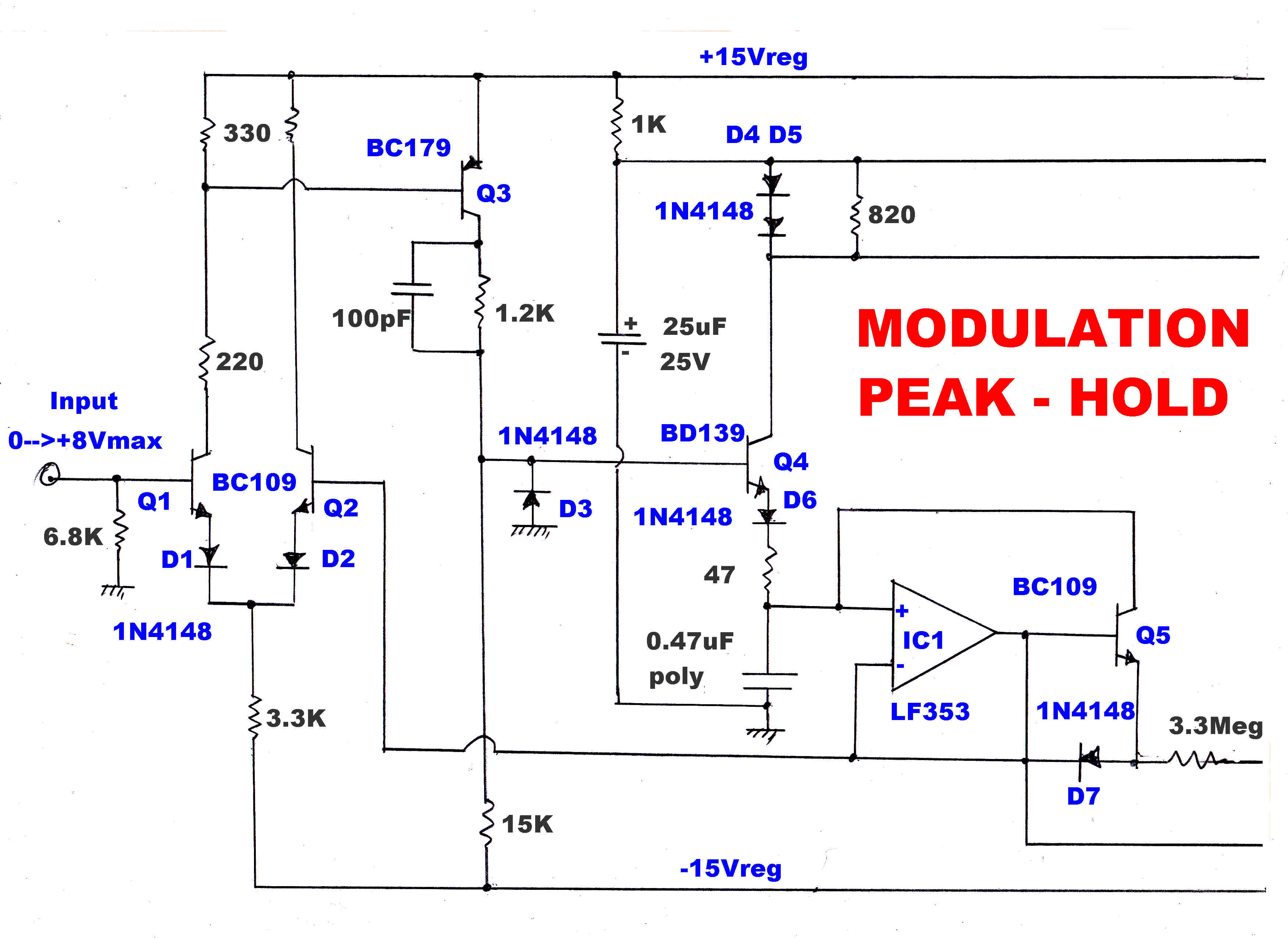
Both the positive and negative peak modulation is stored and presented on
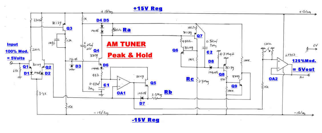
a meter for a few seconds. The circuit for the peak storage is shown above.
A positive going transient on the input turns Q1,Q3,Q4,D5 on, and C1 rapidly charges with
a current limited by the series 47 ohm resistor.
The amplifier OA1 has a very high input impedance with unity gain.
When the voltage across C1 equals the peak input voltage, the long tail pair Q1 and Q2
becomes balanced and C1 ceases to charge. It is left stranded at the peak voltage, since
the charging current cannot reverse through D6.
The charging current develops a voltage across Ra. This triggers the monostable
Q6,Q7 into the "on" state. This rapidly discharges C2 until the low current through Rc is no longer
able to support conduction and Q6 and Q7 turn off.
C2 begins to charge in a negative direction.
During this time the meter indicates the peak value of the applied signal.
When the voltage across C2 reaches -1.2 volts D8 and Q8 turn on.
The collector of Q9 falls to -15 volts and C1 begins to discharge via Rb,
so the indication on the meter falls linearly to zero.
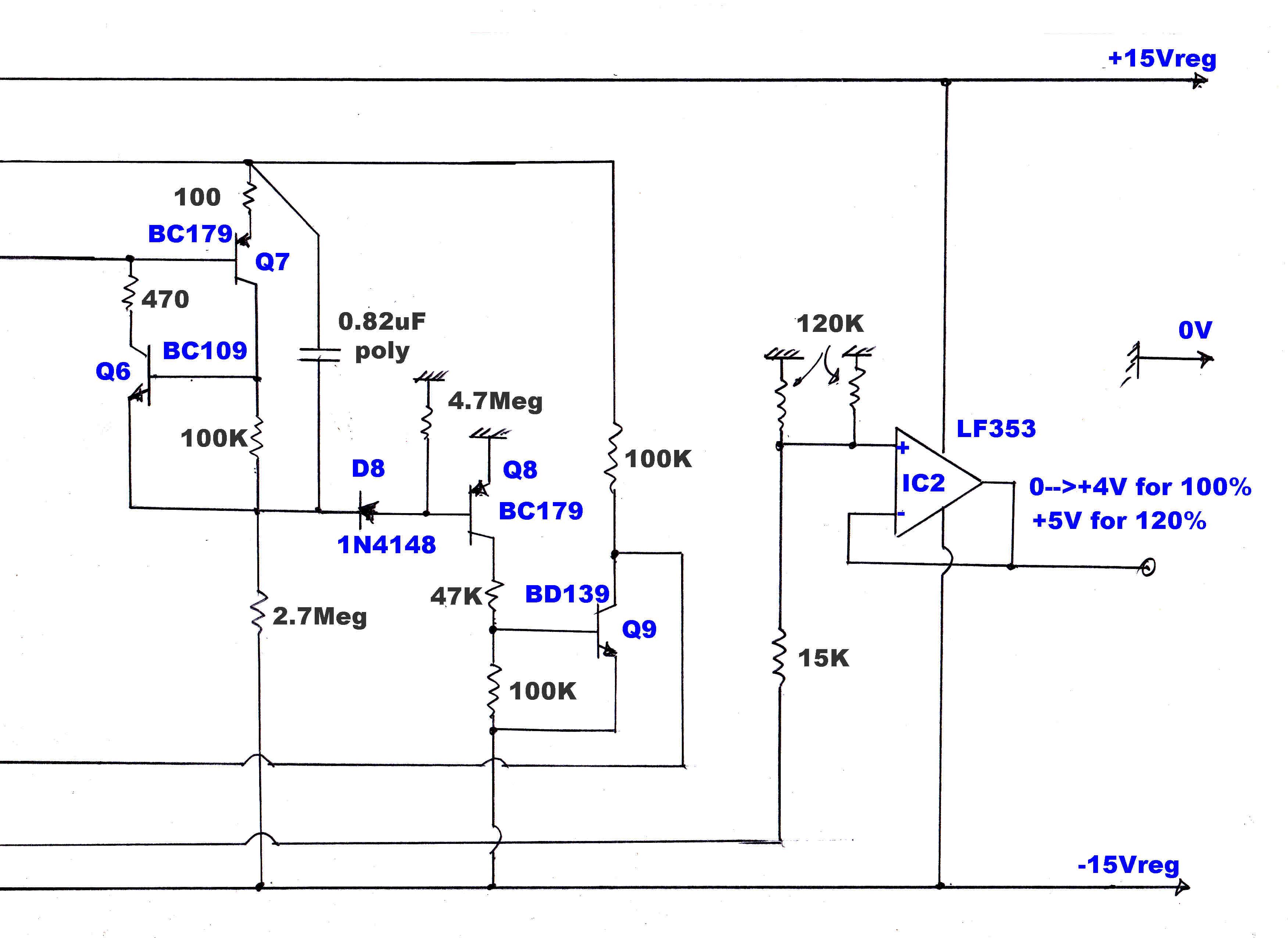
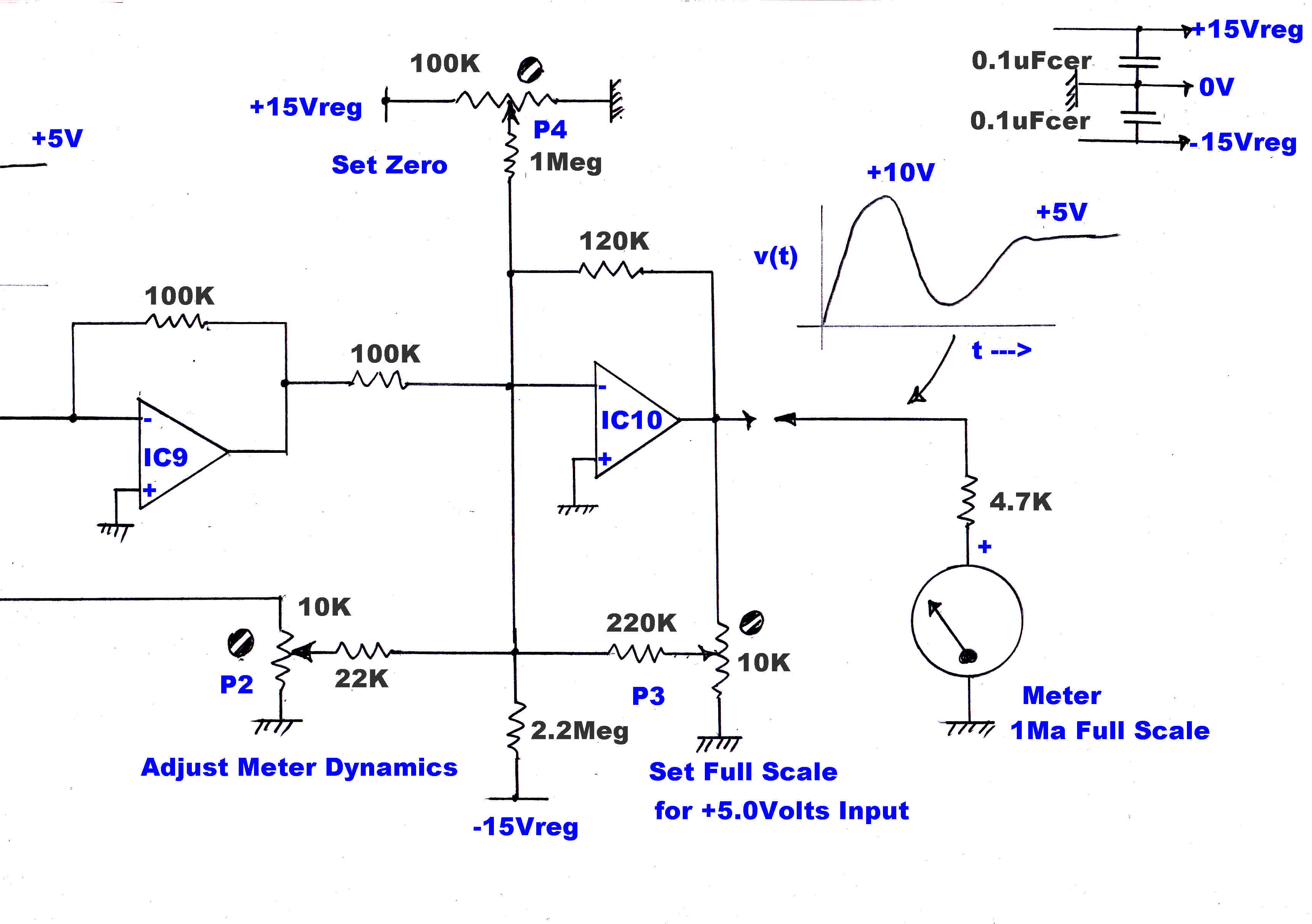
The modulation meter gives full scale at +5volts. Many transmitters now overmodulate in
the positive direction. The resistive attenuator (15k,60k) driving the output amplifier OA2
increases full scale deflection to 125% when peak levels are presented.
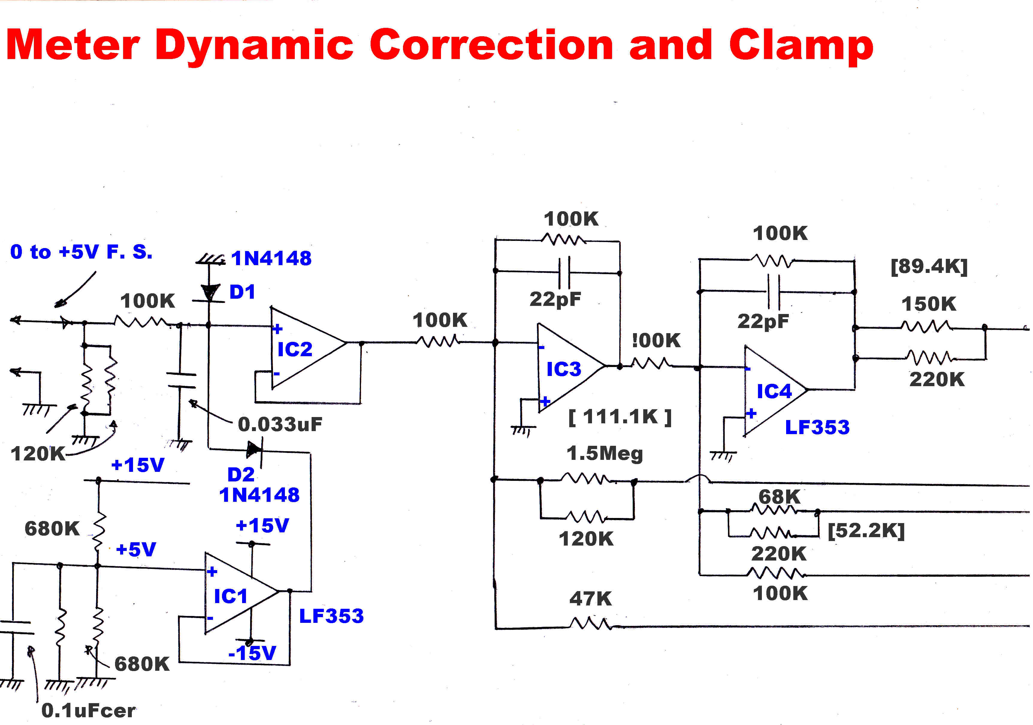
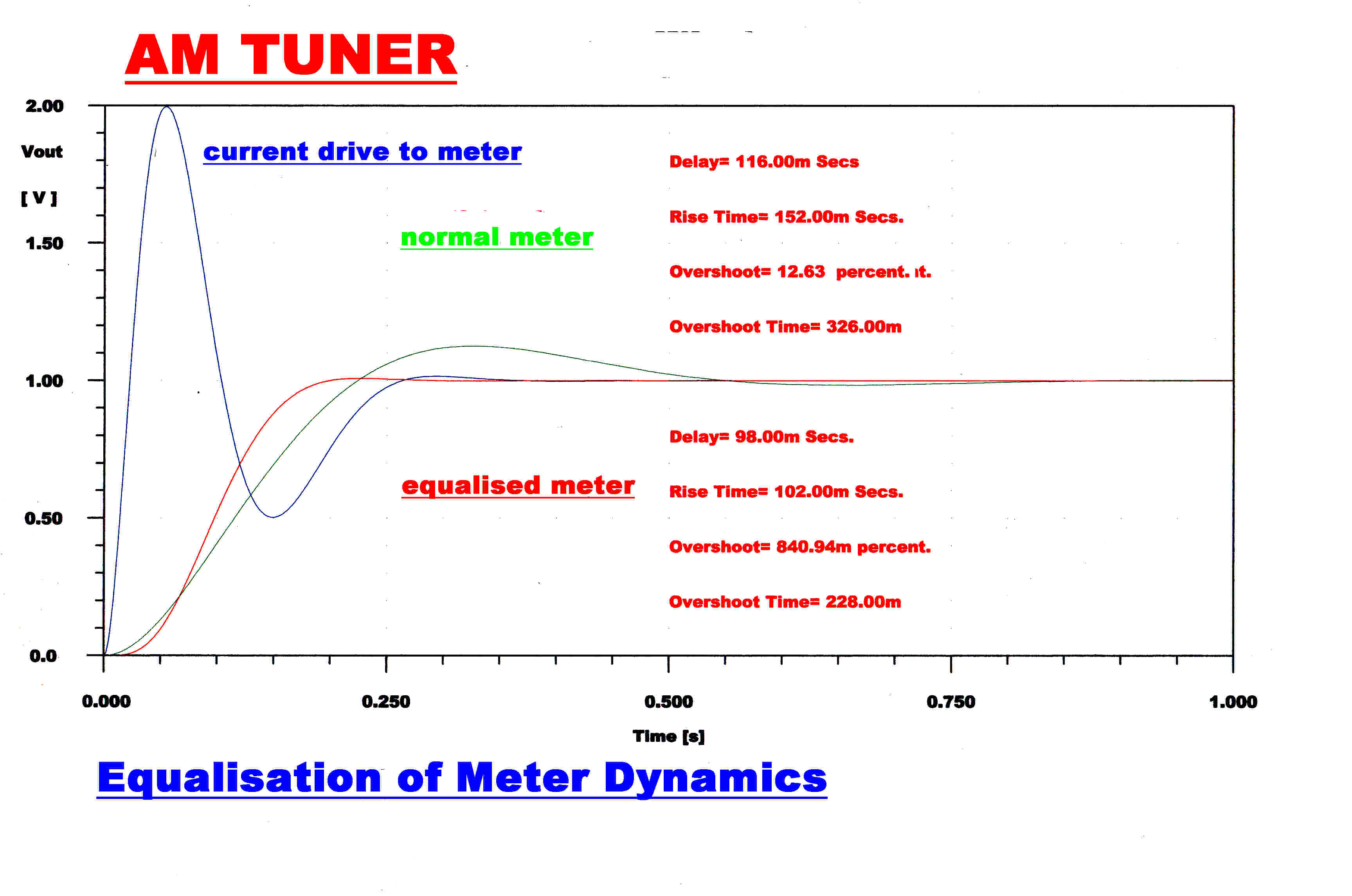 When displaying peak modulation levels, it is highly desirable that the meter
rapidly rises to its final value without noticeable smear or overshoot.
When displaying peak modulation levels, it is highly desirable that the meter
rapidly rises to its final value without noticeable smear or overshoot.
The design of an equalising network to modify the dynamic performance of the meter
will now be discussed.
The transfer function for a typical meter is of the form:-
Y(p) = 1/[ 1 + 2ζτp + τ2p2 ]
where ζ is the damping factor
and τ = 1/ωo
and ωo is the cutoff frequency in radians/sec.
For a typical meter:-
ζ = 0.55 and τ = 8.684x10⁻²
The step function response of a meter with this transfer function is shown in green.
The step function response of a fourth order Bessel transfer function is shown in red.
This has an overshoot of only 0.84% and would give a fast clean meter response.
The poles of a fourth order Bessel transfer function are:-
-1.369776 ±i 0.410163 and -0.994997 ±i 1.256838
This gives a transfer function of the type: 1/D(s) where:-
D(s) = 1 + 2.114168s + 1.915588s2 + 0.8999972s3 + 0.190269s4
If we solve for the step function response we get:-
Delay time, τd = 2.08 Secs.
Rise Time, τr = 2.20 Secs.
Overshoot = 0.835%
Overshoot Time = 4.84 Secs.
Now we want the the rise time of the meter movement to be about 0.1 Secs. so we want
to transform D(s) with the transformation p = s/22. Trials show that the transformation
p = s/21.2766 gives rise to standard values in the realised network. Making this transformation
we get the final required Bessel transfer function 1/Df(p) where:-
Df(p) = 1 + 9.936587x10⁻²p + 4.231532x10⁻³p2
+ 9.343773x10⁻⁵p3 + 9.284512x10⁻⁷p4
The current drive to the meter from the equalising circuit is shown in blue.
A very large initial current pulse quickly accelerates the meter, and then a large negative
undershoot slows it down as it approaches full scale.
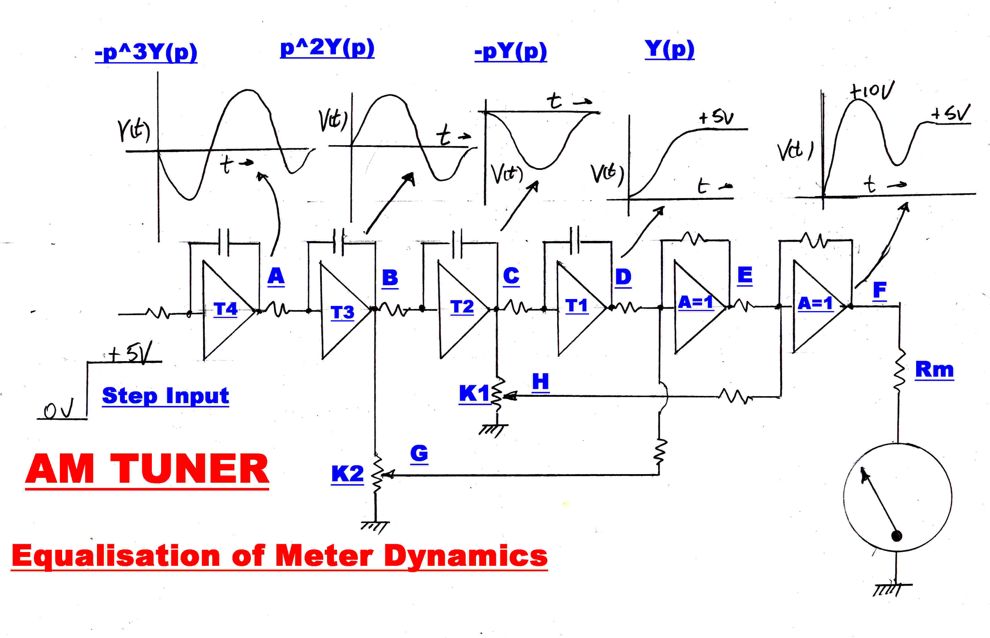 (1) An analog computer program is written to solve for the 4th order
Bessel transfer function: Yb = 1/Df(p)
(1) An analog computer program is written to solve for the 4th order
Bessel transfer function: Yb = 1/Df(p)
(2)This program yields the transfer functions:-
1/Df(p) at D ; -(1/T1 )p/Df(p) at C : and
(1/T1T2)p2/Df(p) at B.
If the first derivative is multiplied by K1 and the second derivative by K2 and then added to
the output, we get the following transfer function :-
Yeq(p) = [ 1 + (K1/T1)p + (K2/T1T2)p2 ]/Df(p)
The overall transfer function including the meter is given by:-
Ytot(p) =
[ 1 + (K1/T1)p + (K2/T1T2)p2 ]/[ 1 + 2ζτp + τ2p2 ]
[ Df(p) ]
If K1 and K2 are adjusted so that:-
(K1/T1) = 2ζτ
(K2/T1T2) = τ2
Then Ytot(p) = 1/Df(p) :: The required result.
Apply a very low frequency square wave to the equaliser and adjust K1 and K2 for the
required Bessel response.
Note: Any meter with a second order transfer function can be accomodated and it is
not necessary to know the meter's transfer function.
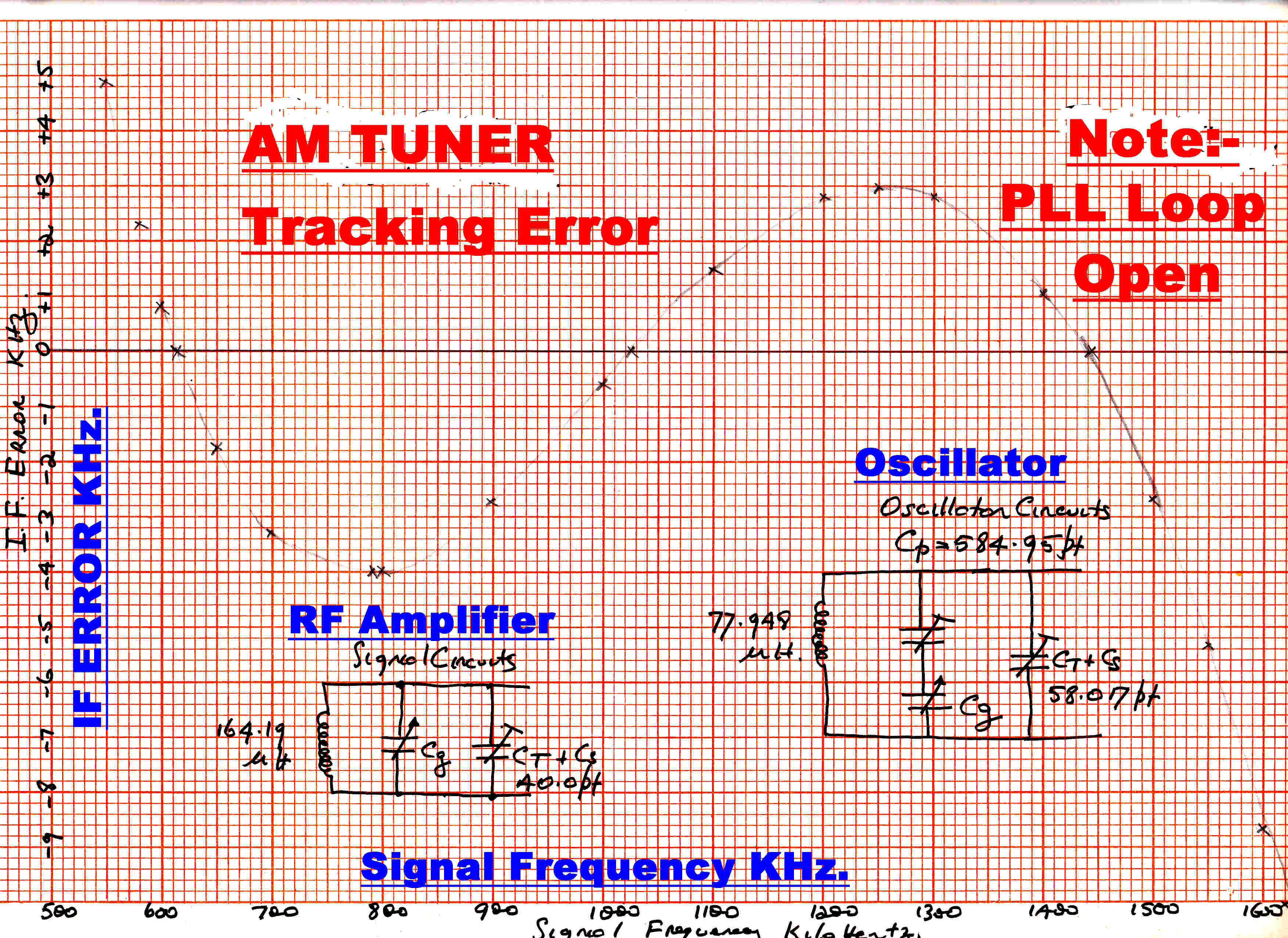 The tuner has three ganged variable capacitors for tuning. Two tune the RF stages and
are tuned to the frequency of the incoming carrier. The third is included in a network to offset
the oscillator frequency 455KHz. above the incoming carrier. Since the oscillator network has
three adjustable elements, there can be three frequencies over the tuning range which give
zero error in the IF frequency.
The tuner has three ganged variable capacitors for tuning. Two tune the RF stages and
are tuned to the frequency of the incoming carrier. The third is included in a network to offset
the oscillator frequency 455KHz. above the incoming carrier. Since the oscillator network has
three adjustable elements, there can be three frequencies over the tuning range which give
zero error in the IF frequency.
A plot of the IF frequency error together with the appropriate networks is shown opposite.
In most tuners the shaft of the tuning capacitor is mechanically coupled to a pointer dial.
The gang capacity plates can be shaped to give a linear shift in frequency with rotation.
Any change in the alignment of these networks requires a change in the coupling to the dial
and the setup is usually a time consuming and frustrating task.
 In the "run" mode the local odcillator frequency is uniquely controlled by the phase locked loop.
A plot of the oscillator frequency against control voltage is given opposite. The control, and hence
the "pull-in" range, is 55KHz., so rotation of the ganged capacitor shaft produces no change in the IF
frequency over this range.
In the "run" mode the local odcillator frequency is uniquely controlled by the phase locked loop.
A plot of the oscillator frequency against control voltage is given opposite. The control, and hence
the "pull-in" range, is 55KHz., so rotation of the ganged capacitor shaft produces no change in the IF
frequency over this range.
For this tuner the only true variable indicating the tuning is the oscillator frequency.
A linear oscillator frequency to voltage converter drives a meter on the front panel to indicate tuning.
This arrangement has the following advantages:-
The Tuning Frequency Scale is Linear
The Tuning Indication is Independent of the Alignment of the RF and Oscillator Circuits
The Tuning Indication is Correct for both "Tune" and "Run" modes.
In the "Run" mode the phase locked loop maintains the IF frequency locked to the crystal oscillator, so
rotation of the ganged capacitor will shift the tuning of the RF stages independently of the oscillator
tuning.
This can be used to eliminate any tracking error, so the RF stages can be tuned for maximum response
and optimum symmetry.
It is appropriate to repeat the tuning instructions given in the INTRODUCTION here.
The tuning of the input RF amplifiers is determined uniquely by the position of
the three gang tuning capacitor, and so may not be centered about carrier.
This is not acceptable, since it will give false results for the quadrature and phase modulation measurements.
The procedure to centre the RF stages is simple:
[A] With the receiver in the "RUN" mode make a small perturbation to the tuning knob.
The phase locked loop is fully active, so no change occurs to th IF frequency.
The AGC loop is in the "SLOW" mode and will not make an immediate correction if there is a change
in signal amplitude due to a change in tuning of the RF stages.
Since there is no correction, the S meter will flick in the direction of change and then resettle
as the AGC loop regains control. This gives a sensitive indication for the direction in which to correct the tuning.
The tuning is centered when a small perturbation of the tuning knob makes no change in the S meter.
Any tracking error is also removed.
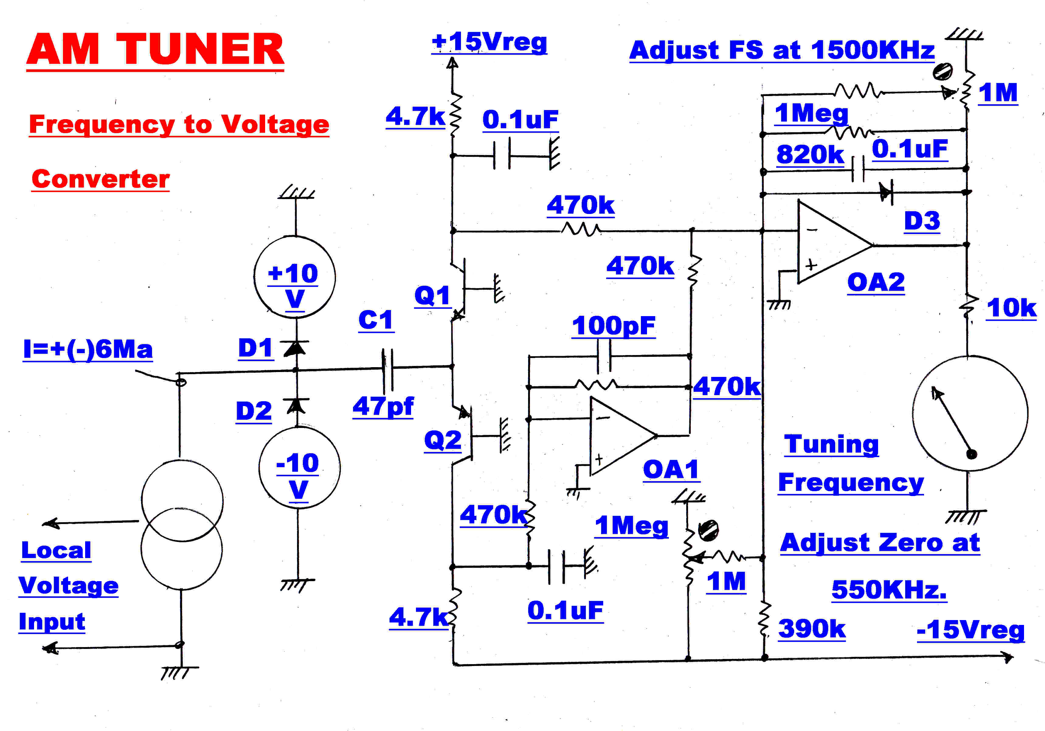 A simplified circuit for the frequency to voltage converter is shown on the right.
The square wave current output from the current generator drives the LHS of C1 into hard clamping
for each half cycle.
A simplified circuit for the frequency to voltage converter is shown on the right.
The square wave current output from the current generator drives the LHS of C1 into hard clamping
for each half cycle.
When D1 is conducting the voltage across C1 is given by:-
V1 = ( 10 + Vd - Ve )
When V2 is conducting the voltage across C1 is given by:-
V2 = -10 -Vd + Ve = -( 10 + Vd - Ve )
where Vd is the diode drop and Ve is the transistor emitter turn on voltage.
For one half cycle the change in voltage ΔV across the capacitor C1 is given by:-
ΔV = 2( 10 + Vd - Vt )
The change in charge ΔQ through C1 is given by:-
ΔQ = CΔV = 2C( 10 + Vd - Ve )
And since this happens twice per cycle the total change in charge per cycle is given by:-
ΔQ = 4C( 10 + Vd - Ve)
At a frequency,f, the total change in charge per second is the current I where :-
I = 4fC( 10 + Vd - Ve )
Now for all temperatures :-
Vd = Ve so that:-
I = 40fC
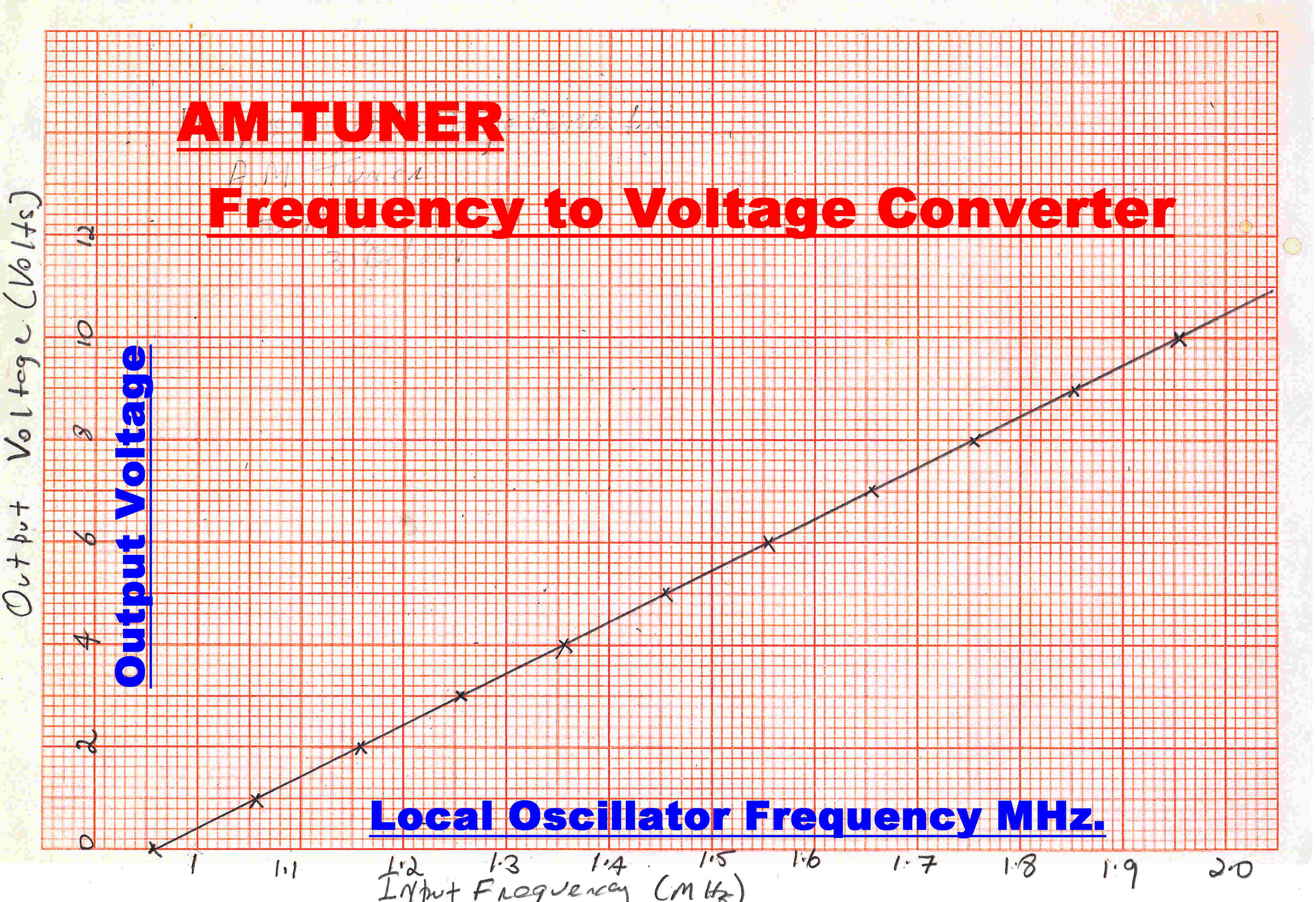
Offset is added so that the output voltage is zero when the frequency is ( 550 + 455 )KHz.
and the gain is adjusted so that the output is 10 volts when the oscillator frequency is
( 1500 + 455 )KHz.
A plot of output voltage versus frequency is shown.
The following audio extract was recorded during daylight hours from the 4QG
(Radio National) transmitter at Bald Hills, Brisbane.
It is the raw output from the tuner and not modified in any way.
Reception Details:-
(1) Bandwidth: ≈ 36KHz. total : effectively 18KHz for modulation content.
(2) Detection: Synchronous Demodulation
(3) Antenna: Indoor Loop
(4) Transmitter Power: Listed as 20KW
(5) Transmitter Distance: ≈ 32 KM
(6) Propagation Path: Ground Wave over built up area.
To hear sound bite No1 click:
SOUND BITE No1
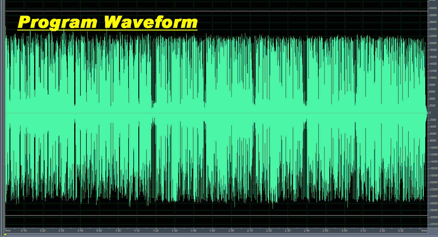
The complete waveform for the sound bite is shown above.
Note that the peak level of each section - whether speech or music - is the same.
This indicates a very high level of signal processing before modulation at the transmitter.
The tuner is equipped with LED alarms to indicate modulation levels above 97%
( both positive and negative ).
These remain "ON" almost continuously.
This example illustrares the enornous change in philosophy in AM broadcasting since
the forties and fifties.
Then the ABC music program was radiated from 4QR - a 10KW transmitter on 590KHz.
with the same monopole antenna used to radiate the above example.
The only signal processing was a peak limiter - no compressor amplifier.
The modulation level was lower to accomodate the odd peak.
The transmitter was heavily modified by the local PMG engineers and, with the addition
of heavy envelope feedback, gave a response well
above the audio range and low distortion.
The studio - transmitter link was baseband open wire line.
Some direct studio broadcasts using an RCA ribbon microphone were particularly memorable.
Program was shared with an FM transmitter. The AM transmitter came out well in comparative tests.
|
|
|
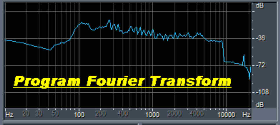
The Fourier Transform of the sound bite is shown above. |
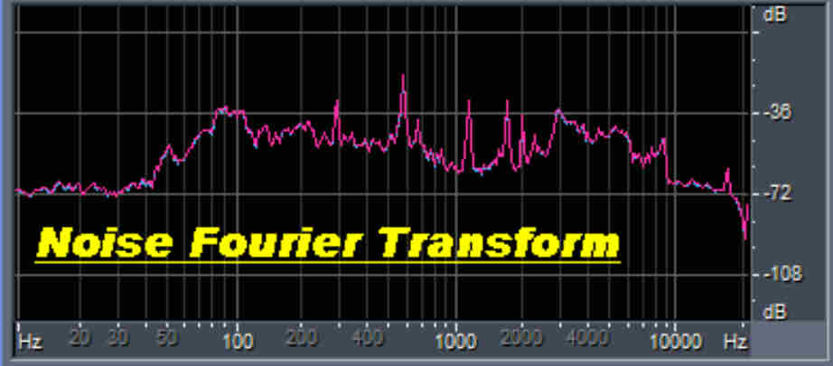
A Fourier Transform of the noise in the sound bite is shown. |
To hear sound bite No2 click:
SOUND BITE No2
[A] Amplitude and Phase Asymmetry
An AM carrier usually contains some phase modulation as well as the
intended amplitude modulation.
The phase modulation can be produced by two distinct mechanisms:-
As shown below, this produces a signal with an in-phase carrier modulated by
P(t) and a quadrature carrier modulated by Q(t).
Both P(t) and Q(t) are related to the original modulation M(t) by a linear differential
equation: so they are linear functions of M(t) and carry NO distortion.
A more detailed discussion is given in the "INTRODUCTION".
The modulation envelope E(t) is given by:-
E(t) = [ (P(t))2 + ((Q(t))2 ]1/2
This is a non-linear process, and so an envelope detector will produce distortion.
The output of a product detector D(t) is given by:-
D(t) = P(t)cos(θ) + Q(t)sin(θ)
where θ is the injection angle of the locally generated carrier.
Since both P(t) and Q(t) are both linear functions of M(t) there is no distortion.
Note:The asymmetry of a matching network or radiator usually increases with deviation
from the carrier, so this type of distortion usually increases with modulating frequency.
The phase modulation θ(t) is given by:-
θ(t) = tan-1[ Q(t)/( 1 + P(t) )]
[B] Non-Linear Processes within the Transmitter
ACTIVE ELEMENTS
Phase modulation can be caused by non-linearity in an active element and is
best explained by a typical example.
In vacuum tube transmitters a PI matching network was frequently placed in the grid of the final stage.
Variation in grid current over the modulation cycle produced a variable load at carrier frequency,
and so phase modulation.
This effect is not sensitive to modulation frequency, and so appears at low modulating frequencies.
It causes distortion in product detectors.
PASSIVE ELEMENTS
Passive elements may suddenly change their value over the modulation cycle and so
produce a step function of phase modulation.
This corresponds to a delta function of frequency modulation.
The transmission network, especially the narrow band IF in the receiver, acts as a frequency discriminator
and turns the phase modulation back into amplitude modulation resulting in horrendous distortion
in an envelope detector.
Transmitter monitors are usually wide band and may not respond to this phase modulation, so the effect can go unnoticed
CASE STUDY
A vacuun tube 50KW transmitter was situated about 32KM from this site.
Distortion would start at about 11AM - reach a maximum at about 1PM - and then suddenly stop at about 2PM.
The distortion was least on a wide band tuner and worst on a narrow band communications receiver -
the reverse of what would normally be expected. The symptoms pointed to step phase modulation.
Contact with the transmitter indicated that it did not appear on the station monitor - a 5AR4 full wave power rctifier
driven by a pickup loop near the final and very wide band.
My only suggestion was that it could be due to flashover of one of the inductors in the matching hut on modulation peaks.
This proved not to be the case.
The distortion persisted for some weeks and was eventually tracked down to the substitution of the vacuum tube Xtal oscillator
with a solid state unit using a high frequency Xtal and frequency divider.
The bypassing and shielding of the divider were inadequate and the divider was miscounting with RF pickup from the 50KW final.
The divider trigger level was temperature sensitive and occurred only in the hottest part of the day.
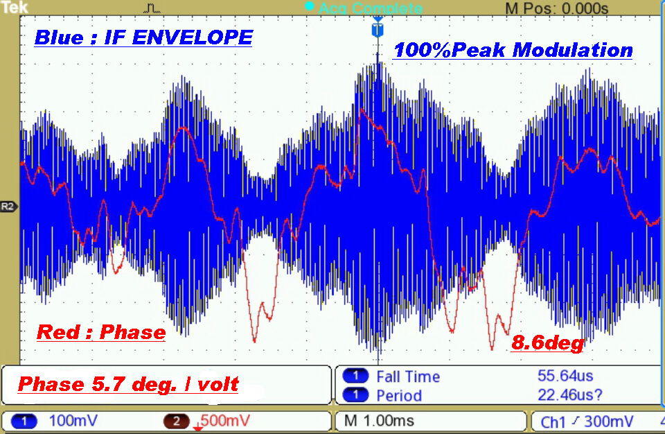
The phase modulation on two of the local AM broadcast transmitters is shown below.
Consider the expression for the phase modulation θ(t):-
θ(t) = tan-1[ Q(t)/( 1 + P(t) )]
Here P(t) the inphase and Q(t) the quadrature modulation are normalised.
With present practice P(t) → -1 on negative modulation peaks and can reach +1.2 on positive modulation peaks.
Since the denominator ( 1 + P(t) ) → 0 on negative peaks, [ Q(t)/( 1 + P(t) )] can → ∞ ,
so that, even with a small quadrature component Q(t), the phase deviation θ(t) can be large.
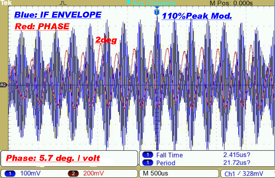
Test Results on 4QG 792KHz(RN)
This is a 20KW transmitter with a single monopole radiator.
The transmission path is about 32KM over a built up area.
The receiving antenna is a non-resonant loop.
The receiver is operated with its maximum bandwidth of 36KHz.
|
|
|
The transmitter is modulated fairly heavily at about 1.8KHz, yet the phase deviation
is below 2 degrees. |
This illustrates the expected phase modulation transient on a negative modulation peak. |
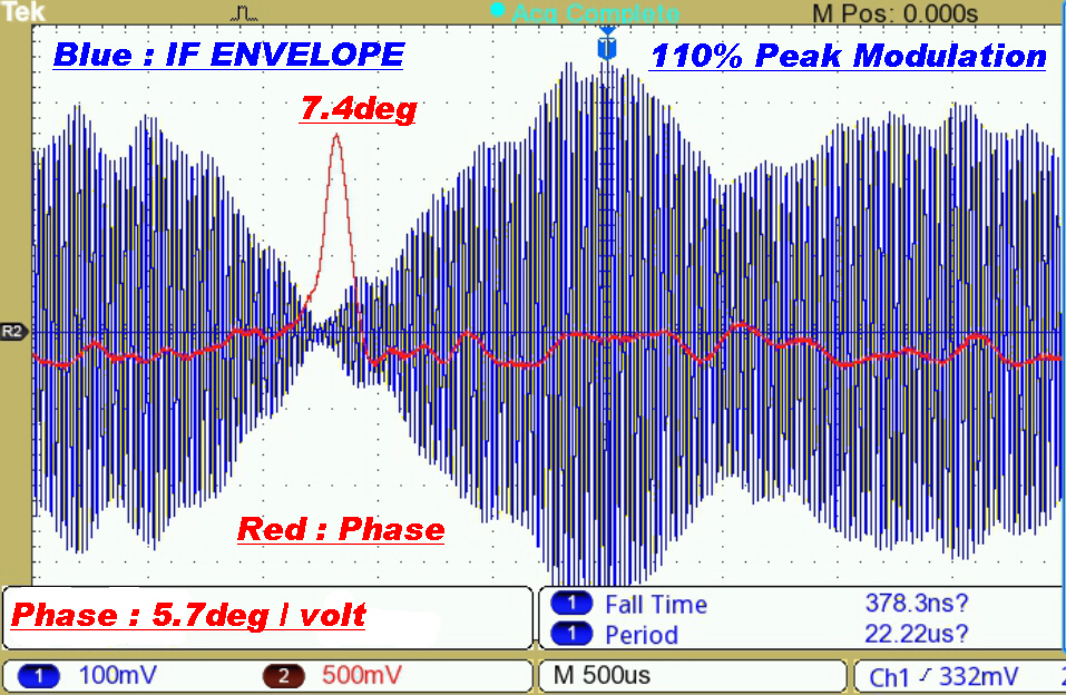
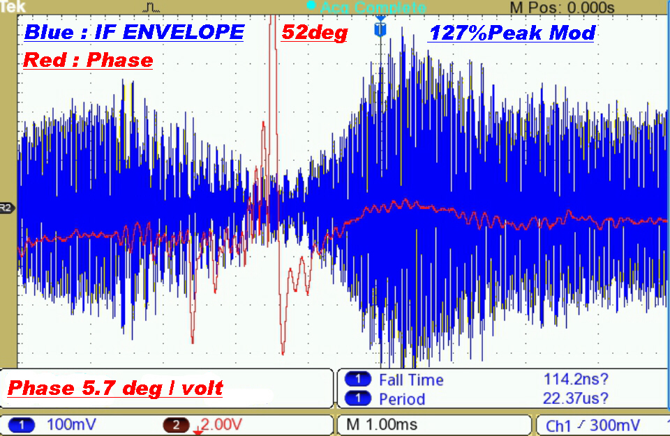
Test Results on a Commercial Transmitter
Distortion was noticeable on an envelope detector and even worse with a product demodulator.
The audience for which the "music" was intended would probably regard the distortion as a bonus.
|
|
|
A phase deviation of 8.6 degrees on a signal modulated at 330Hz can only be explained by non-linear effects in the transmitter. |
Here the transmitter is modulated very heavily. |
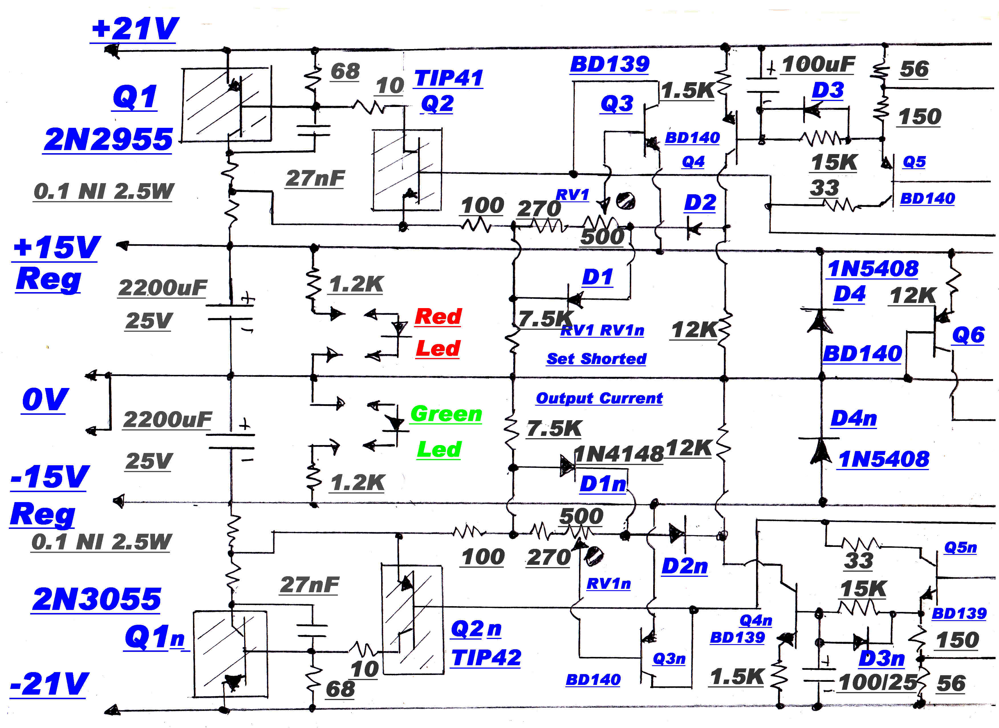
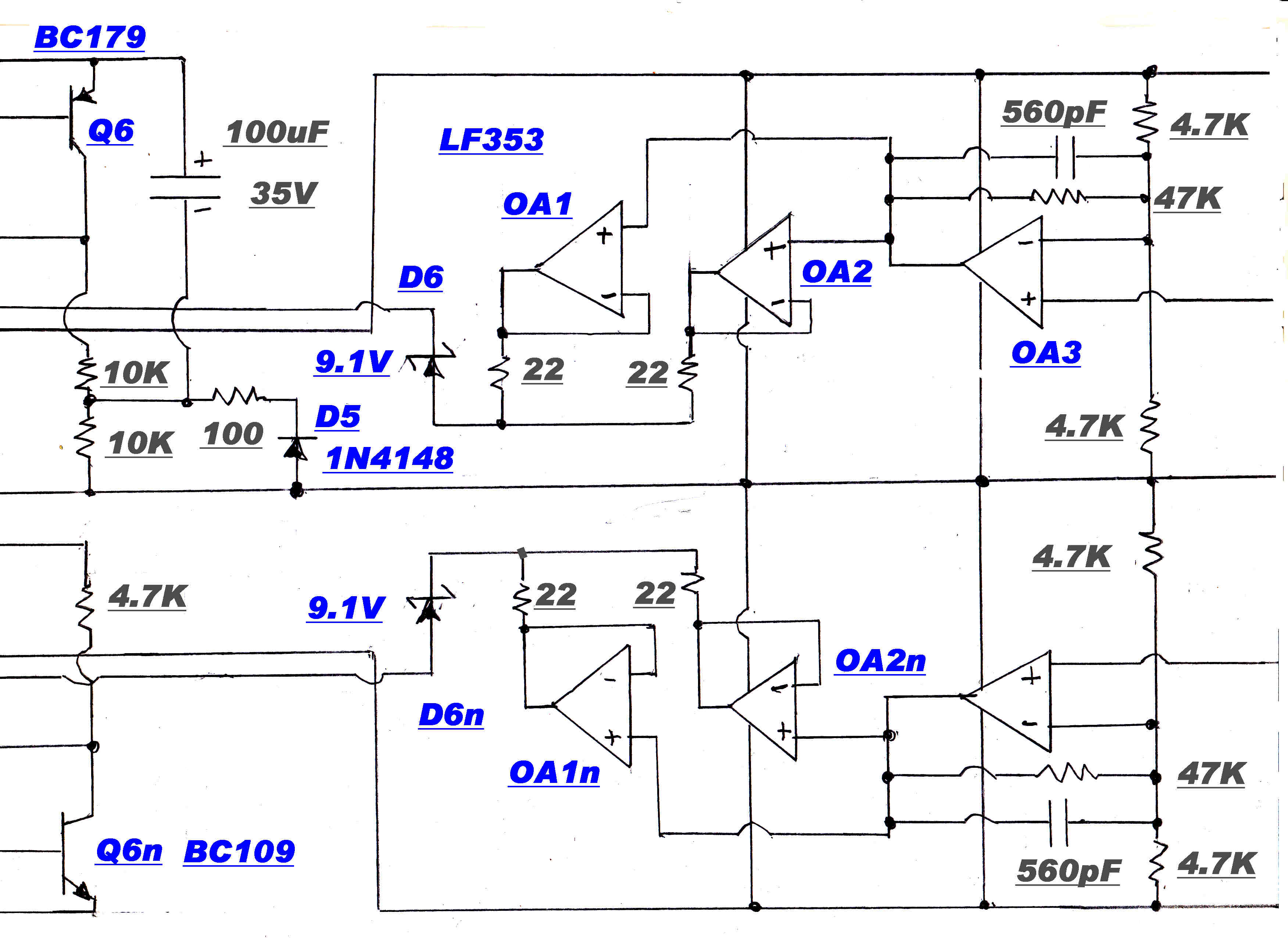
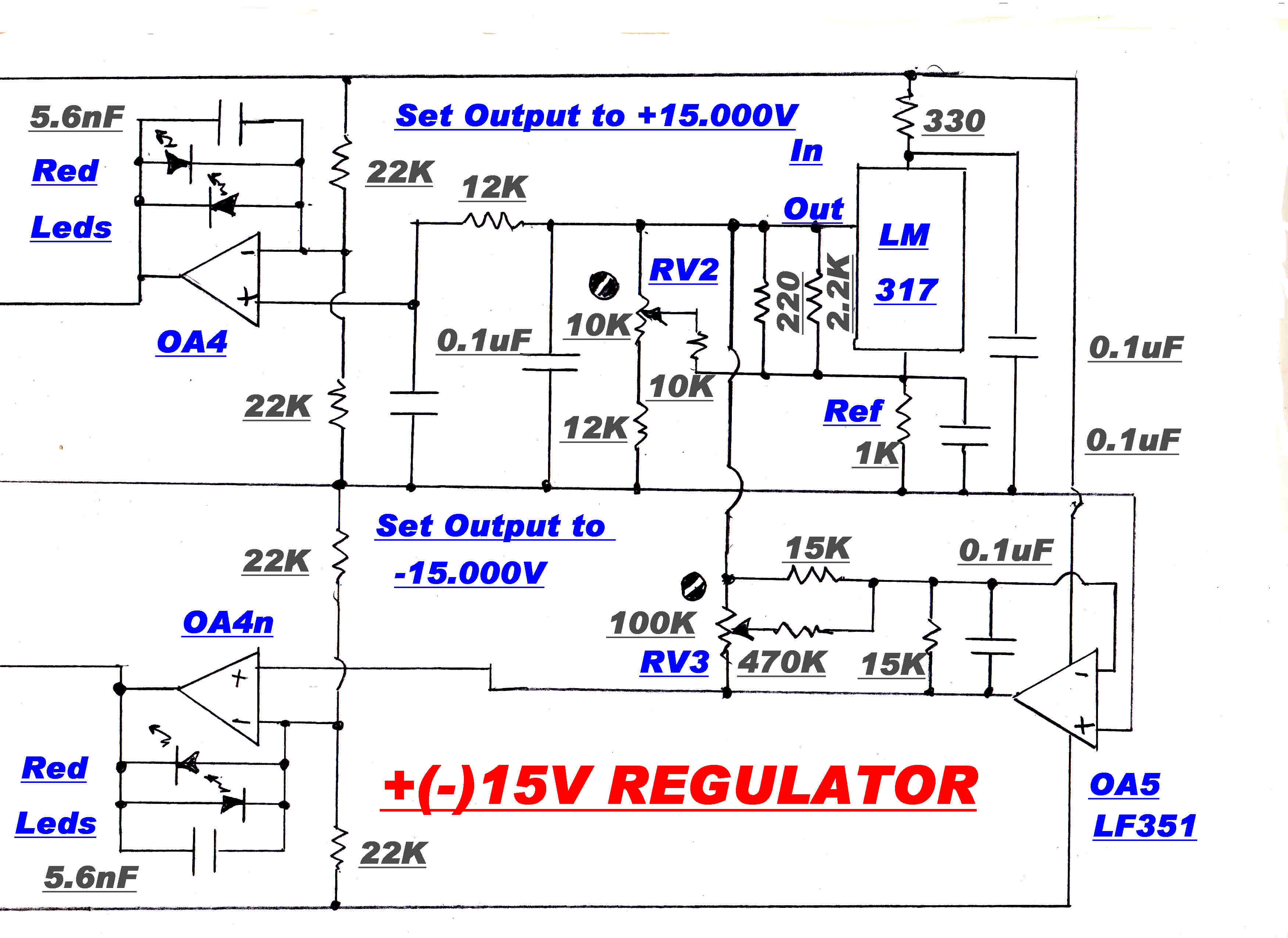
The regulator powers all the low level stages of a large solid state audio system.
Its maximum output of +(-) 5 amps far exceeds the demands of the tuner.
It is designed to have a "soft" start - that is a slow run up on turn on. This limits the chargng current into the
many bypass capacitors on the rails.
Q5 and Q5n provide the "on" drive to the output stage. The 100uF - 10k network in its base causes the
collector currents to rise slowly to their full value.
The current limit at start is about 6 amps and this increases to about 8 amps at full voltage.
After some delay, Q4 and Q4n turn on and reduce the short circuit current to a small value, and so reduce the
dissipation in the pass transistors Q1 Q1n Q2 Q2n.
The regulator uses a high gain slow speed feedback loop and a low gain high speed loop.
This technique was discussed in detail in the vacuum regulator section.
The complete circuit of the power supply is shown below:
REGULATOR
|
|
|
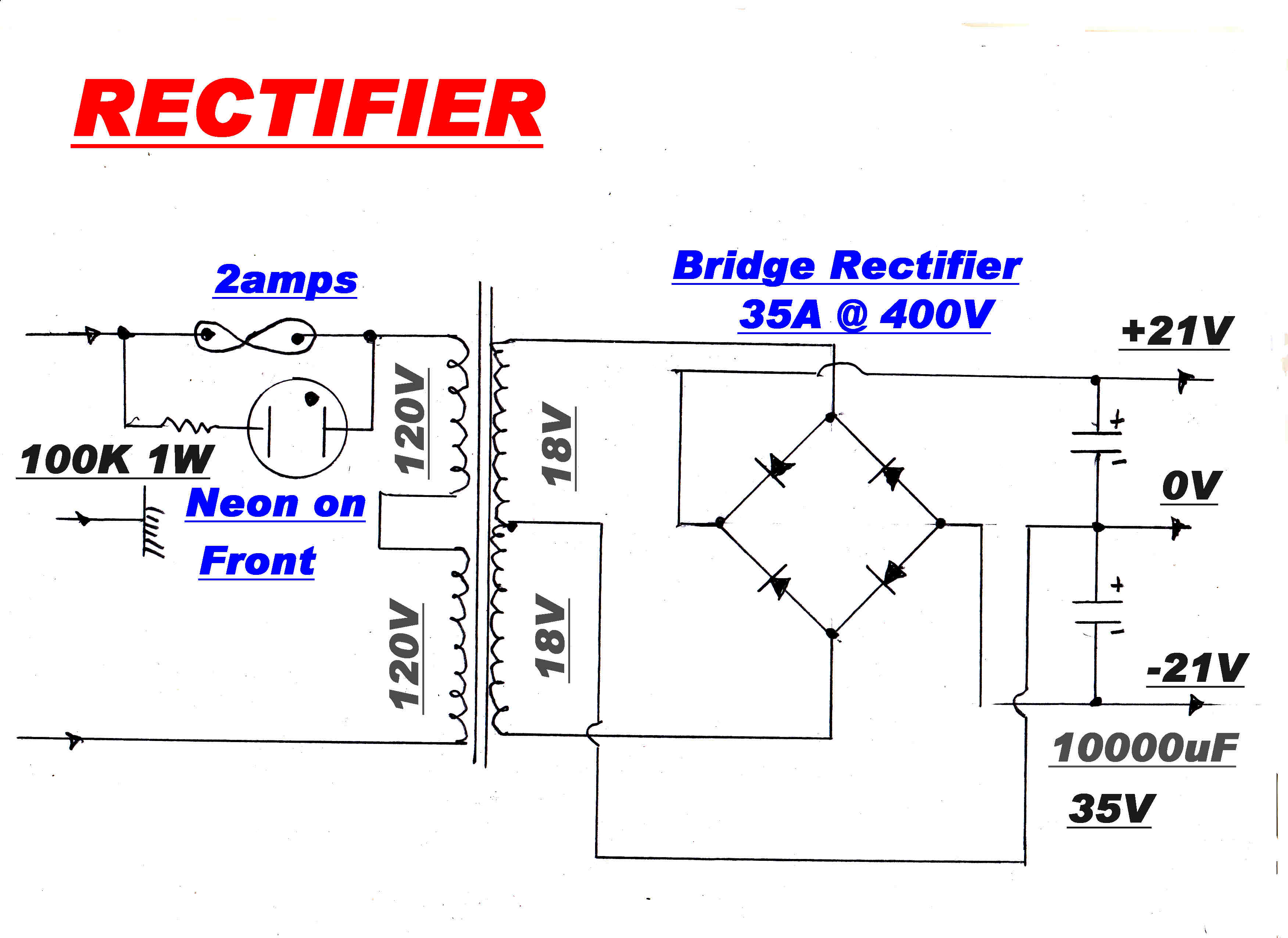
RECTIFIER

|
|
|
|
|
|
|
|
|
|
|
|
|
|
|
|
|
|
|
|
|
|
|
|
|
|
|
|
|
|
|
|
|
|
|
|
|
|
|
|
|
|
|
|
|
|
|
|
|
|
|
|
|
|
|
|
|
|
|
|
|
|
|
|
|
|
|

|
|
|
|
|
|
|
|
|
|
|
|
|
|
|
|
|
|
|
|
|
THE FOURTH ORDER GAUSSIAN RESPONSE |
METER TRANSIENT RESPONSE |


|

|
|
|
|
|
|
|
|
|
|
|
|
|
|
|
|