6L6 VACUUM TUBE AMPLIFIER

CONTACT : COMMENTS AND QUESTIONS
back/home
The amplifier is based on the design philosophy
and architecture used in the 6V6 amplifier.
See the 6V6 Amplifier
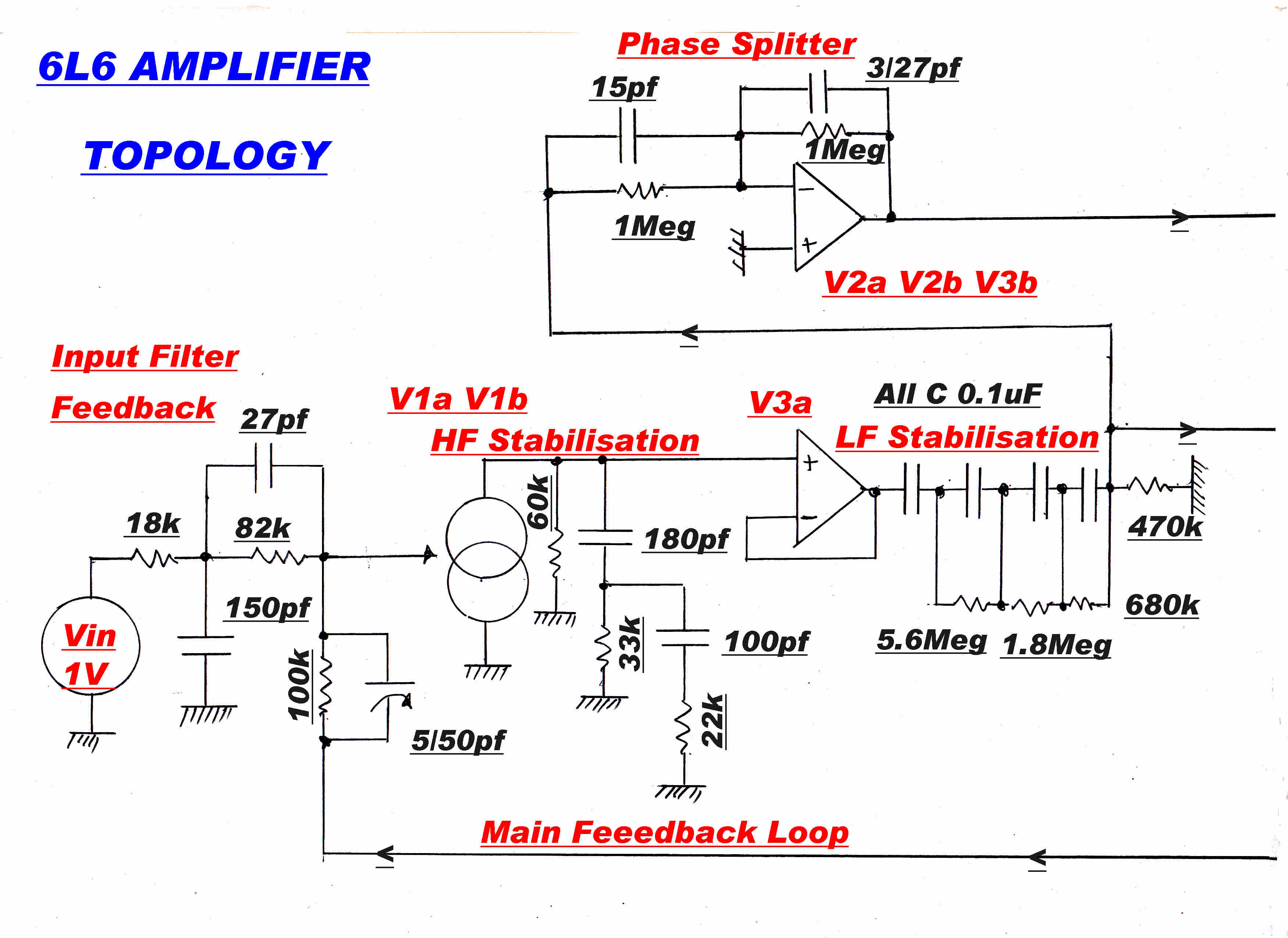
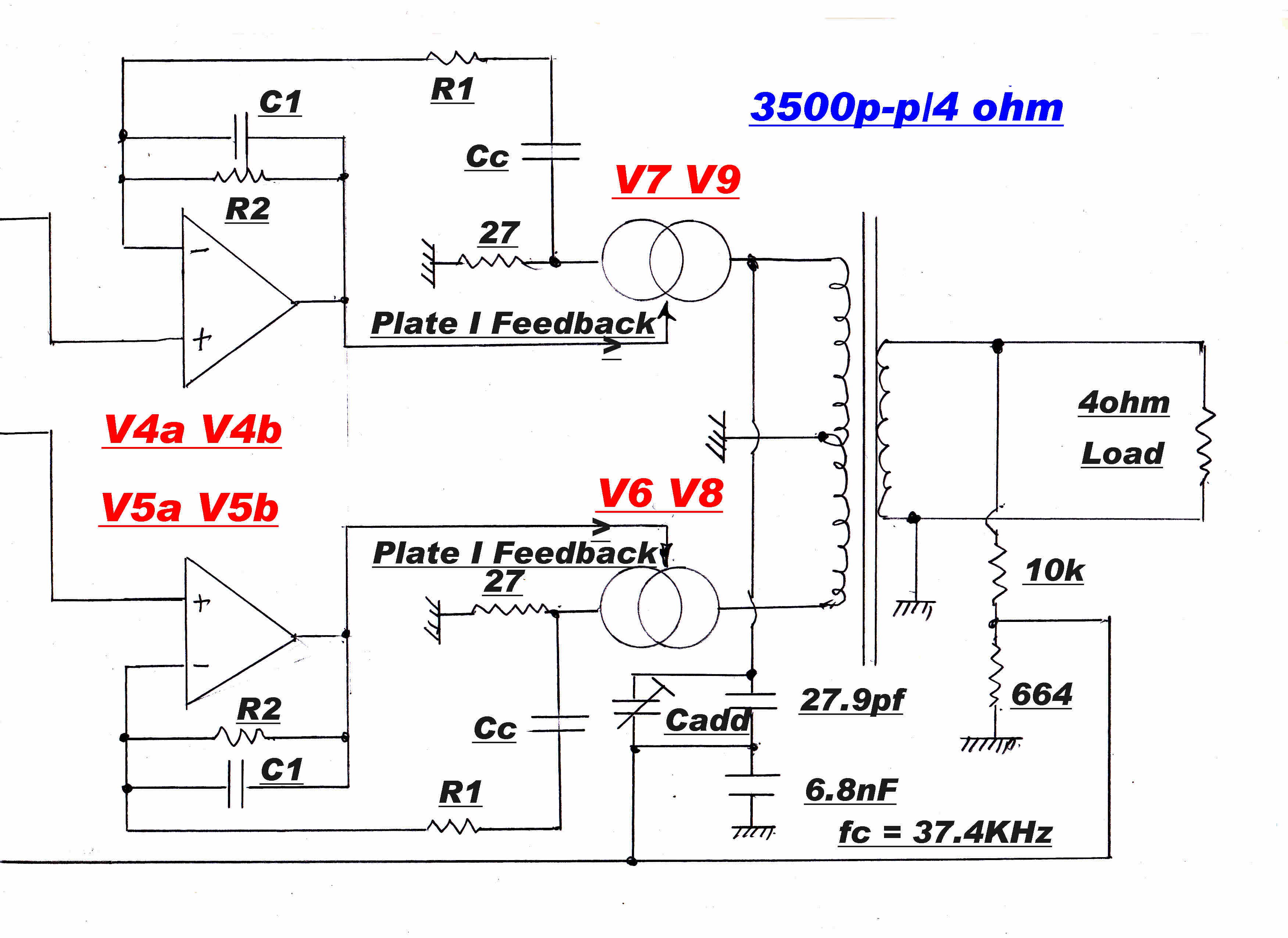
A simplified diagram is shown below:-
|
|
The total plate current on either side of the push-pull class A amplifier is sensed
in a 27 ohm resistor. This provides about 20 db of feedback over the 6L6 output tubes.
Extra plate current feedback is produced by the 120 ohm unbypassed cathode resistors.
The result is:-
[1] The distortion in the output stage is reduced by a factor greater than 10.
[2] The output impedance is high - virtually infinite for all practical purposes.
[3] The low frequency and high frequency response of this inner loop is tailored to achieve
a transfer function which aids stability in the overall feedback loop.
The low frequency turnover is about 0.5Hz and the high frequency turnover about 500KHz.
This takes it outside the active frequency range of the main feedback loop.
[4]The effective Gm of the output tubes is stabilised.
The initial preset balance of the push-pull amplifier holds for long periods.
This is aided by the long term stability of the phase splitter which is an operational amplifier
with high gain.
Note that the amplifier does not rely on "matched" tubes or their freedom from drift.
[5] In almost all class A push-pull amplifiers the drive on the grids of the output tubes produced
by the phase splitter is symmetrical -
the drive on one grid is the negative of the drive on the other grid.
The peak positive drive is equal to the peak negative drive.
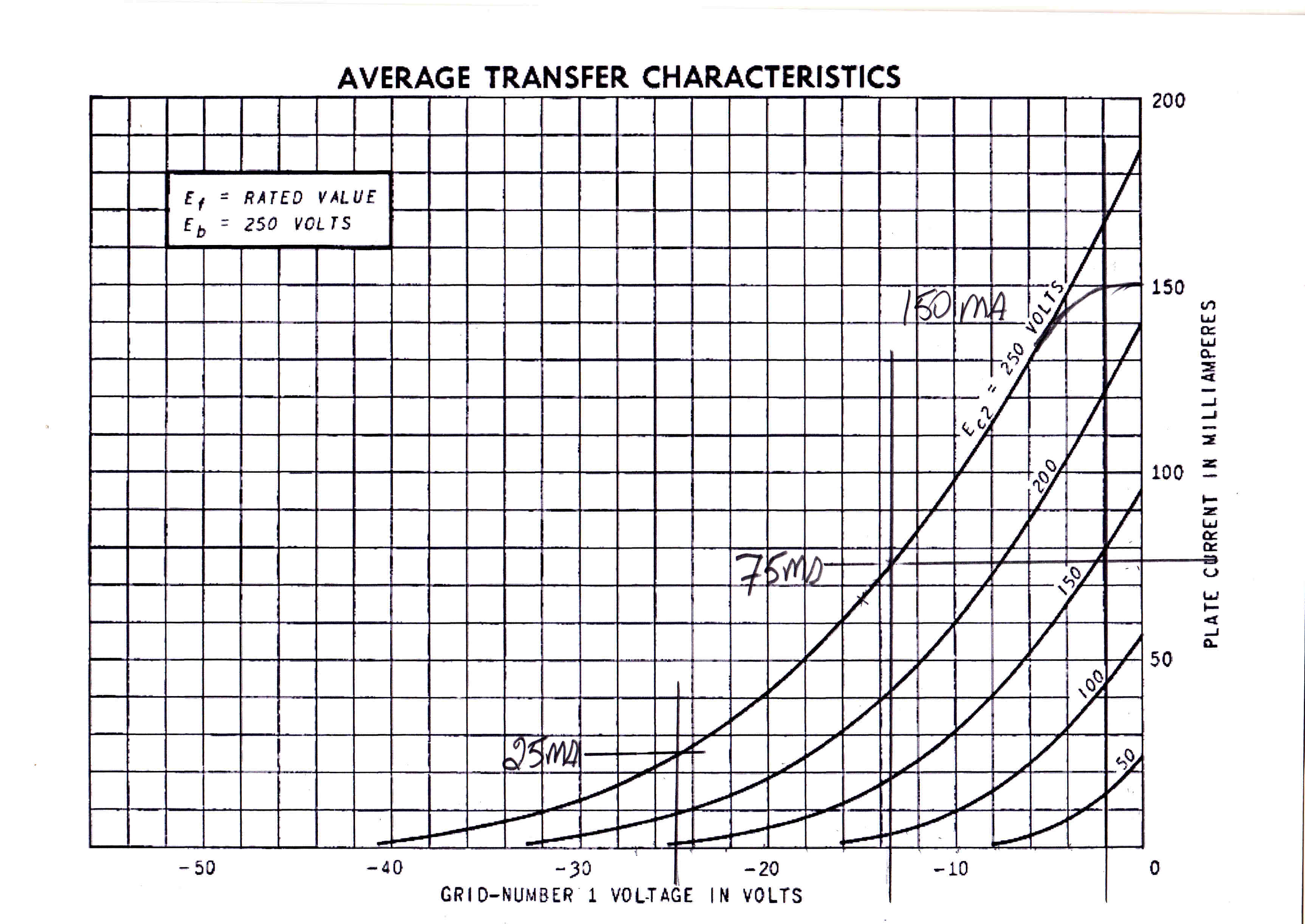
The transfer characteristic ( Ip/Vg) of the output pentodes (6L6/6V6) is a square law.
They require a much greater negative voltage swing on the grid to turn off than on the positive cycle
which drives the grid to zero volts.
The result is that the output tubes are never cutoff with a consequent waste of power.
The high degree of feedback in the current loop produces an asymmetric voltage drive to
the grids of the output tubes.
This ensures that the output tubes cutoff at full power output.
|
|
|
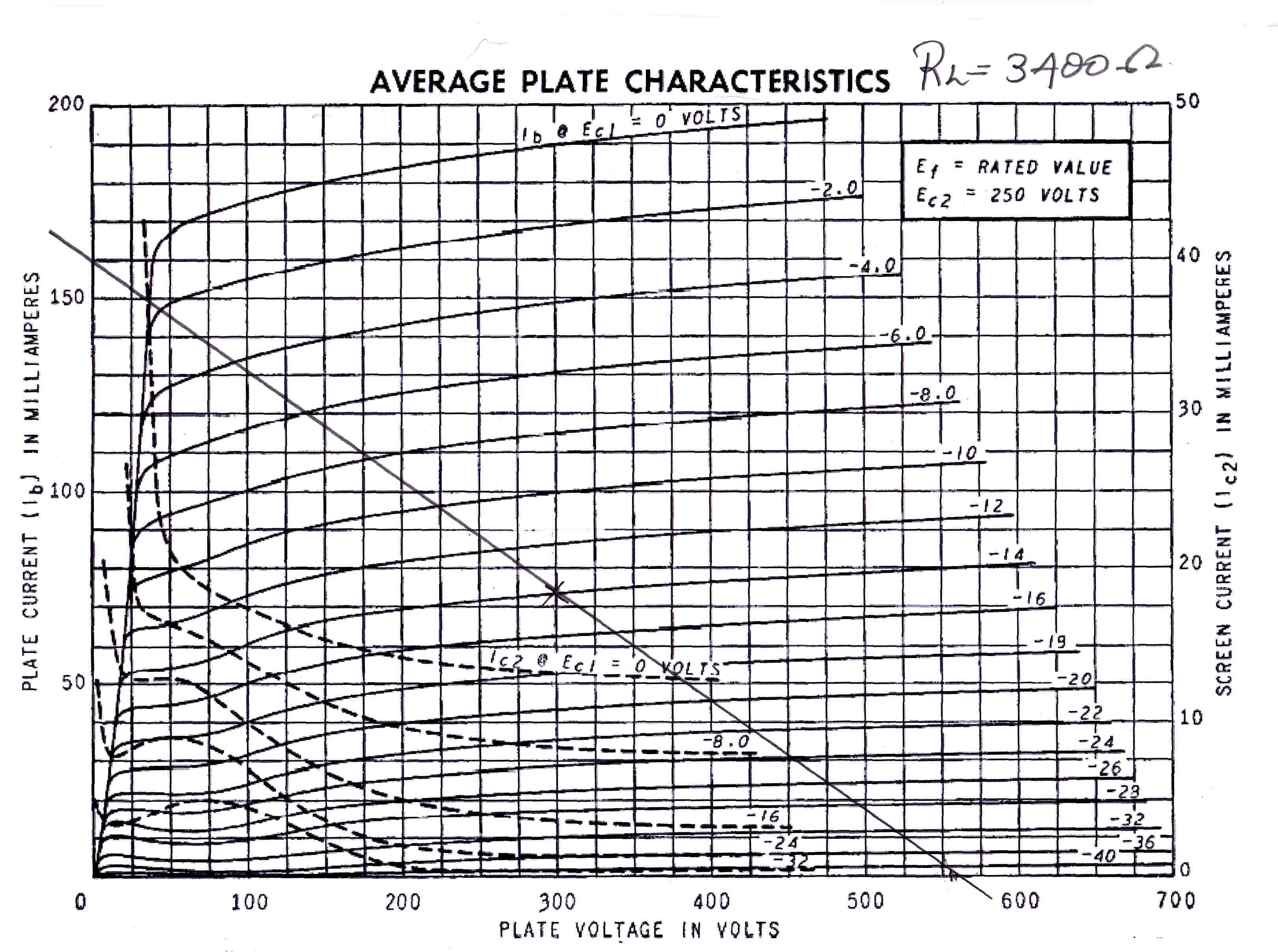
6L6 PLATE CHARACTERISTICS |
6L6 TRANSFER CHARACTERISTIC |
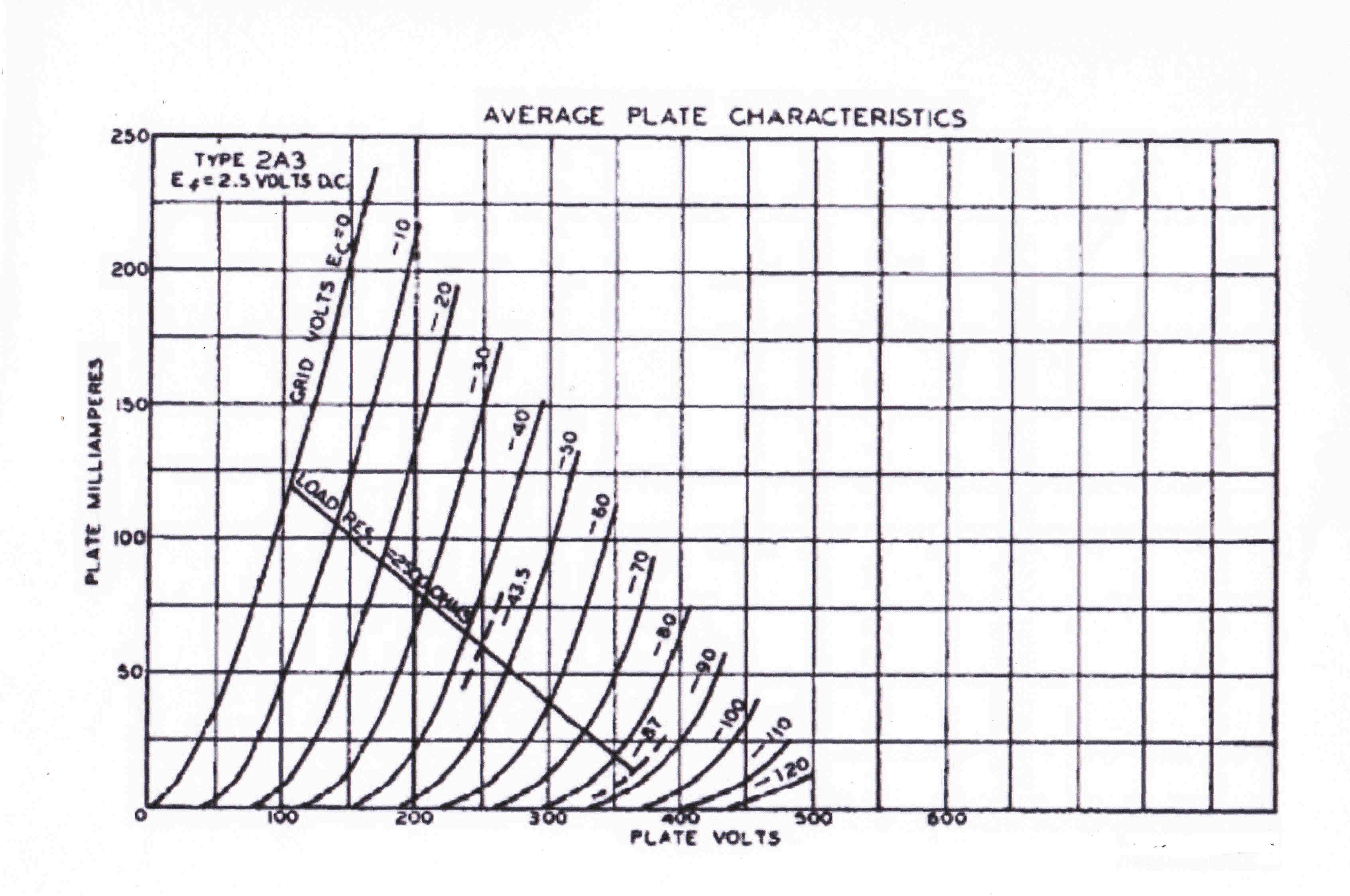 The plate current characteristics for a triode output stage are more linear than those for a pentode.
The effect still exists in a triode output stage.
The curves for a 2A3 triode are shown opposite.
A quiescent plate current of 62.5Ma reduces to a standing current of about 15Ma on the negative half cycle with symmetrical drive.
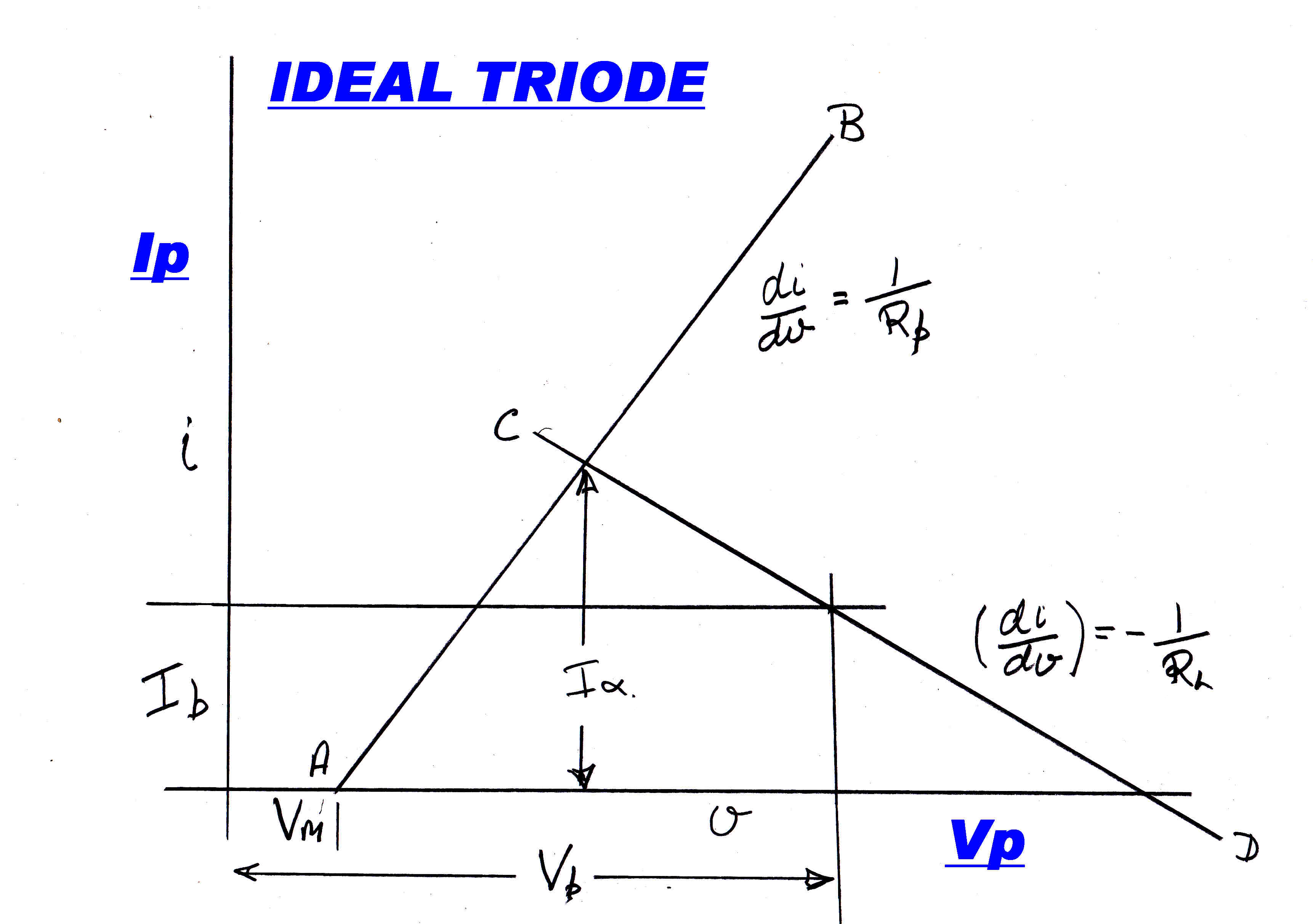 For a triode it is possible to choose a load line to give symmetry
Consider the idealsed triode plate curve shown opposite.
Let AB be the linearised plate current curve for zero grid volts.
CD is the load line with a load RL
The quiescent operating point is:-
Plate Voltage = Vb
Plate Current = Ib
For AB:
v = Vm + i Rp ------------(1)
For the load line CD :
v = Vb + ( I - i ) RL -----------(2)
To find Iα equate (1) and (2)
Vm + Iα = Vb + ( Ib - Iα ) RL
Iα = ( Vb - Vm + IbRL )/( Rp + RL )
The positive increase in plate current ΔI + is given by:
ΔI + = Iα - Ib
= ( Vb - Vm + IbRp )/( Rp + RL )
The negative current swing ΔI - is given by:
ΔI - = Ib
For symmetry:
ΔI + = ΔI -
So:
Ib = ( Vb - Vm + IbRL )/( Rp + RL )
Giving:
RL = ( Vb - Vm )/Ib - 2Rp
For symmetry:
RL = ( Vb - Vm )/Ib - 2Rp
EFFICIENCY
The output power Pout is given b y:
Pout = 1/2 Ib2 RL
The input power Pin is given by:
Pin = VbIb
So:
η = 1/2 [ 1 - Vm/Vb -2 Rp/( Vb/Ib ) ]
To increase efficiency in a triode choose a large Vb and a small Rp
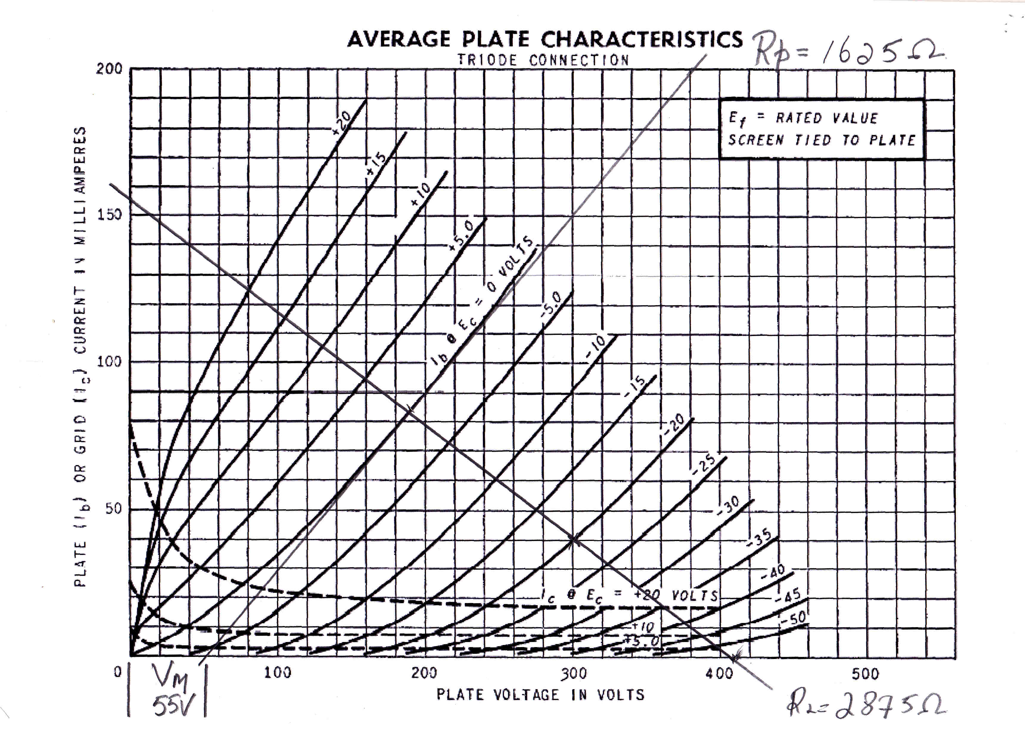 A triode connected 6V6 with a symmetrical load line is shown opposite.
Here:
Vm = 55V
Rp = 1625 ohms
Vb = 300 volts
Ib = 40Ma
RL = 2875 ohms
ΔVmax = 115 volts
η = 0.192
The large gain around the current feedback loop produces an asymmetric drive on the grids of the
6L6 output tubes.This contains a DC component.
For short transients the operating conditions on the driver do not change. If the amplifier is forced to produce full output
for a prolonged period, the operating conditions on the driver (DC plate current - grid bias) change. This is accompanied by
a slow speed transient in the current feedback loop.
This is characteristic of all AC coupled systems with non-linear elements.
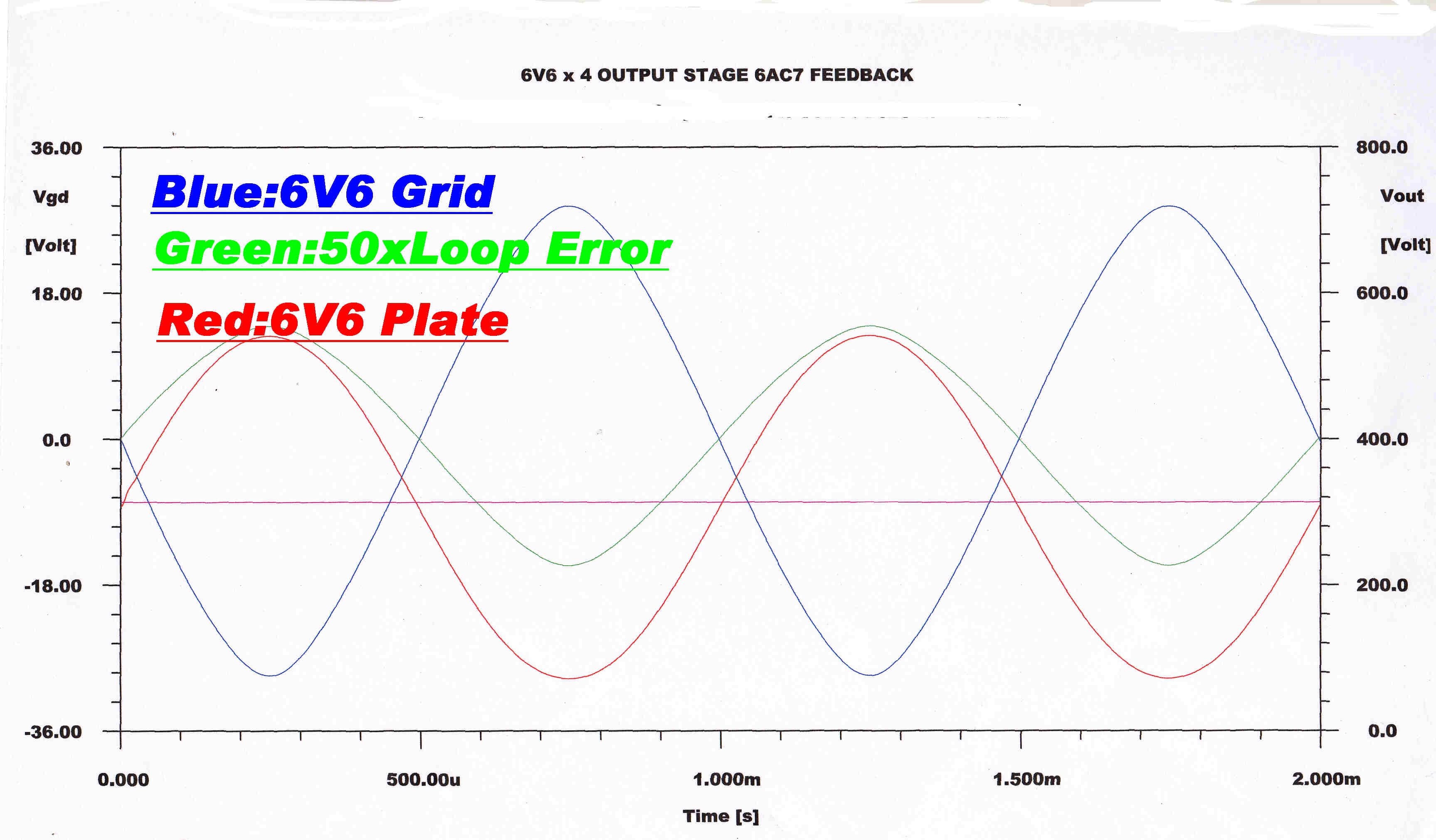
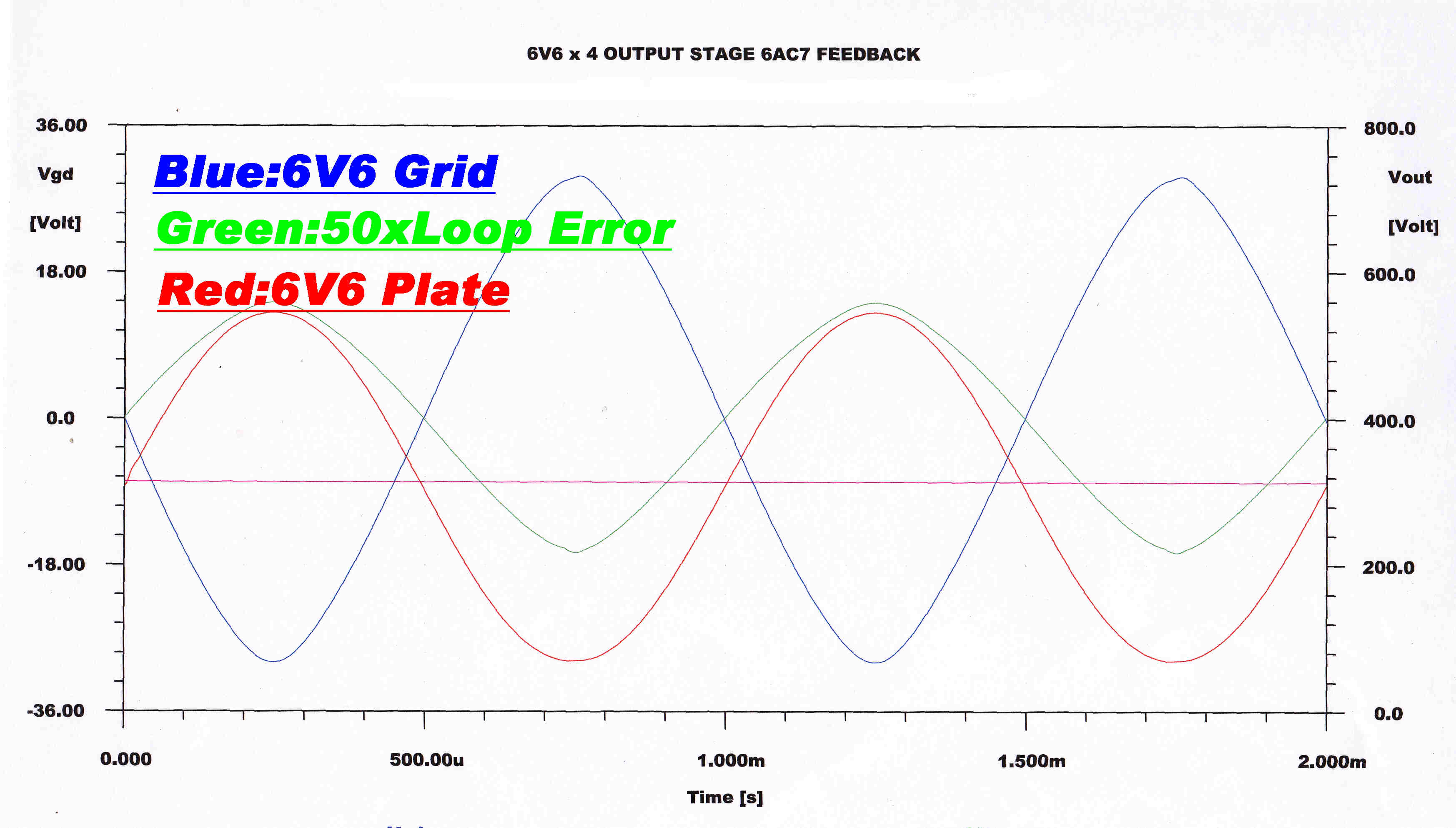
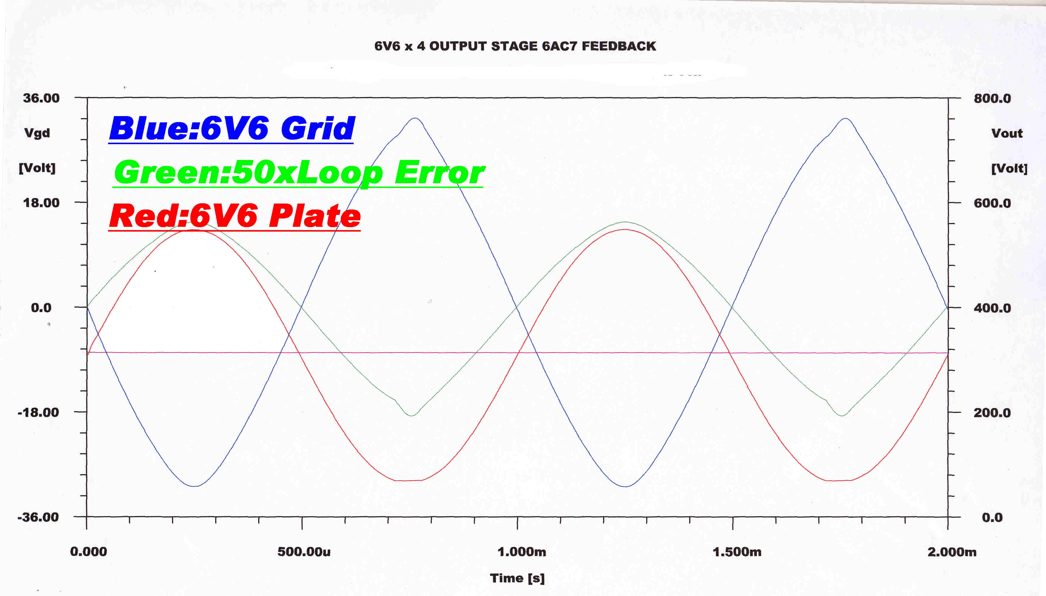
The plate (output) voltage, the grid drive and the current loop error are shown below
for the following conditions:
[A] Just before full power output
[B] At full power output
[C] Just after overload
|
|
|
|
Just before full power |
At full power |
Just after overload |

An oscillogram taken with the amplifier approaching full power output.
Yellow--Grid Drive
Blue - Cathode Voltage --[Cathode and Plate Current ]
Red - Grid to Cathode Voltage
The tight current feedback loop around the output stage produces a large negative spike in order to approach cutoff.
The cathode voltage across the cathode resistor produces a cathode current which is sinusoidal, indicating low inherent distortion in the output stage.
Note: The cathode current equals the plate (output) current because of the screen bypassing.
The unbypassed cathode resistors in the output stage stabilise the quiescent plate current and
linearise the transfer characteristic.
The magnitude of DC transients in the current feedback loop is reduced.
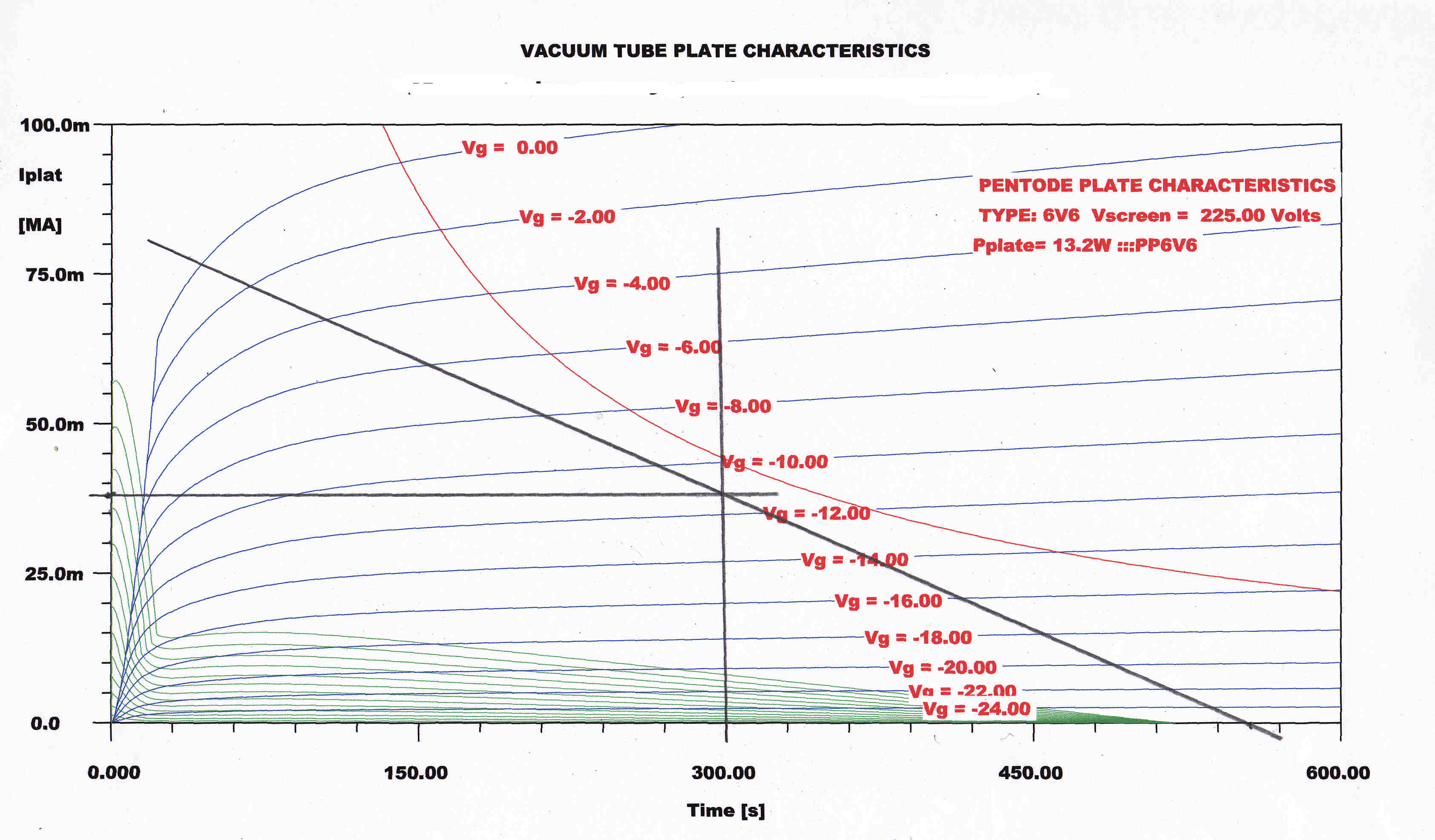
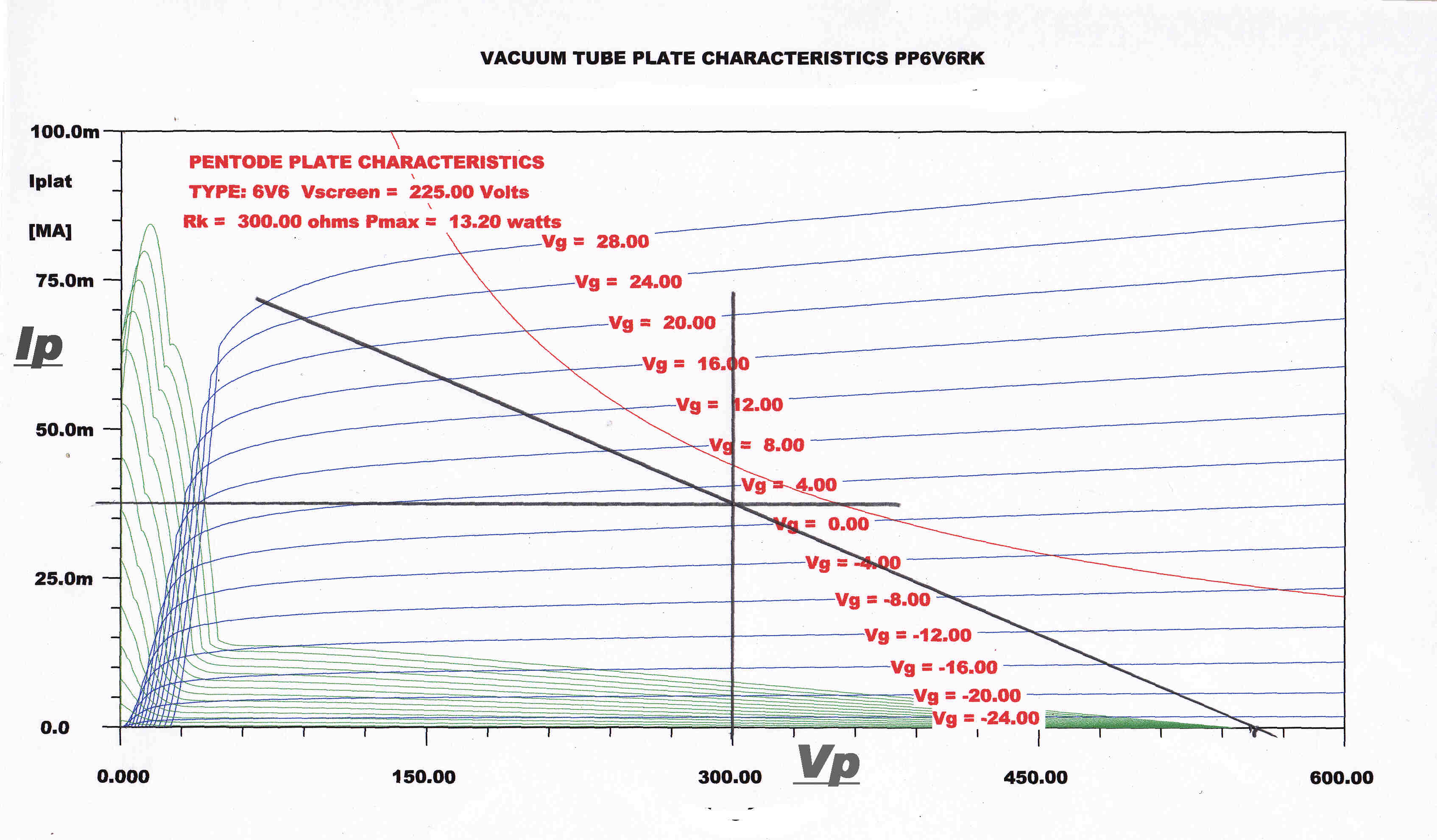
The output tube with the cathode resistor can be regarded as a tube with linearised characteristics.
The plate characteristics for such a tube together with those for the raw tube are shown below.
|
|
|
BEAM TETRODE PLATE CHARACTERISTIC |
PLATE CHARACTERISTIC WITH UNBPASSED CATHODE |
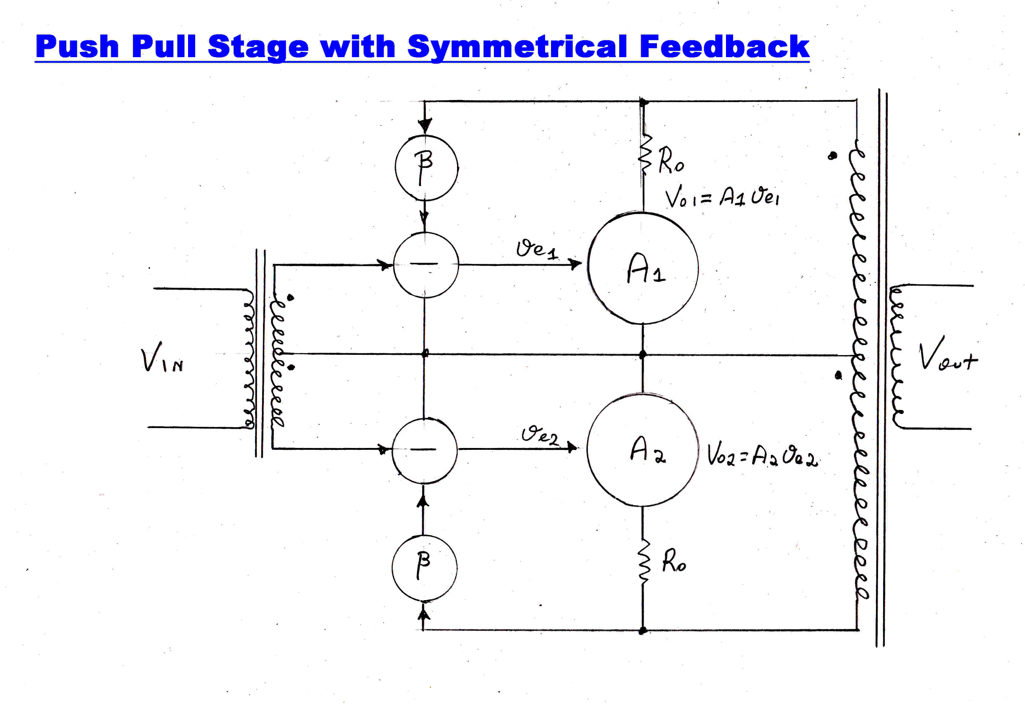 The block diagram of a push pull output stage with symmetrical feedback loops
is shown opposite.
It has been found that this topology gives rise to amplifers in which the output
stage balance is very sensitive to the drive balance.
It is also sensitive to component drift within the loop: a parameter which negative feedback
should be reducing - not increasing.
We now investigate the reason.
If we tease the circuit apart, it will be seen to be two feedback amplifiers sharing
a common load: in other words two feedback amplifiers in parallel.
Now the feedback reduces the output impedance of both amplifiers, so in reality, we have
two low impedance generators in parallel: a classical combination for poor load sharing.
The load on each amplifier is a parallel combination of the load Rl and the output impedance
of the other amplifier, which can be quite low because of the feedback. The gain of each
side for unbalanced inputs is therefore much lower than the common mode gain: the loop error
and hence the unbalance will be greater.
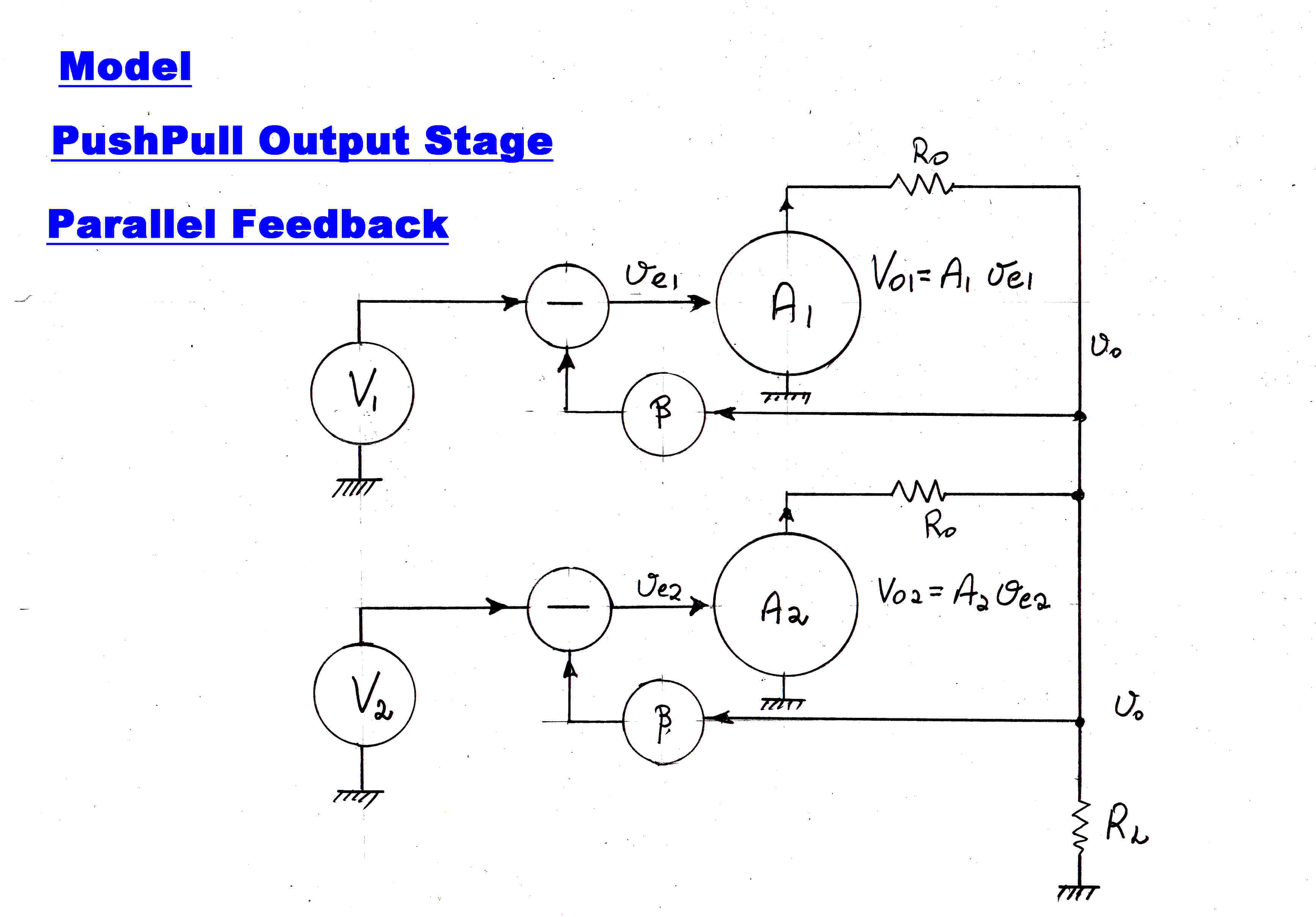 We now analyse the error signals in a push-pull stage with symmetrical feedback
from either side of the output transformer.
To simplify the algebra, and to emphasise the fact that two feedback amplifiers
are in parallel and sharing a common load, we redraw the amplifier as shown.
The push-pull amplifier now reduces to two feedback amplifiers in parallel.
The inputs are now in phase not push-pull.
If we apply Thevenin to the output stage, each output generator has an equivalent voltage of
V/2 with an putput resistance of Ro/2.
This gives rise to the following identities:-
γ = vo/Vo1 = vo/Vo2
= 1/( 2 + Ro/RL )
We can then write:-
ve1 = V1 - βvo -----------(A)
ve2 = V2 - βvo -----------(B)
vo = γ( Vo1 + Vo2)-------(C)
= γ( A1ve1 + A2ve2)----(D)
ve1 = V1 - βγ( A1ve1
+ A2ve2 ) ------(E)
= V1 - βγA1ve1 - βγA2ve2
------(F)
ve1 + βγA1ve1 =
V1 - βγA2v
From (A) and (B) we get:-
ve1 - V1 = ve2 - V2 ----(H)
ve2 = ve1 - V1 + V2 ----(J)
Substituting (J) in (G) :-
ve1 = [ V1 + βγA2( V1 - V2 ) ]/
[ 1 + βγ( A1 + A2 ) ] -----(H)
Now let us consider what happens when an out of balance push pull drive
is applied to the system.
We can do this by putting V2 to 0 and perturbing
V1 by ΔV1
Suppose each side is balanced, so that A1 = A2 = A
Then, substituting in H, we get:-
Δve1 = ΔV1( 1 + βγA )/( 1 + 2βγA ) --------(J)
[The error on side 1 for an increase in drive on side 1 by ΔV1 ]
The error on side 2:-
We can calculate the error on side 2 (Δve2) by imagining a change in V2 and calculating
Δve1 . This is true because the system is symmetrical and linear.
We have:-
Δve2 = -ΔV1( βγA )/( 1 + 2βγA ) --------(K)
The error on side 2 for ΔV1 on side 1.
For a balanced drive:-
ΔV1 = ΔV2
Again, substituting in H, we have :-
Δve = ΔV1/(1 + 2βγA )----------(L)
The error in each channel for a balanced drive.
We now divide to find the ratio, R, of the errors on each side with an unbalance drive and
a balanced drive:-
R1 = 1 + βγA
R2 = - βγA
R1 is the return difference or the reduction of gain by the symmetrical feedback loops.
|R2| is the loop gain.
If the feedback is large, then a small amount of
unbalance in the push-pull input will cause a much bigger unbalance in the error signal,
and so the drive to the output stages - highly undesirable.
For instance, a 2% unbalanced drive will cause 20% unbalance with 20db of feedback.
This reduces the power output and increases the distortion.
The balance adjustment is much more sensitive and difficult to adjust.
Lesson: If feedback is to be applied over the output stage ( and driver ), then,
it should be taken from a point NOT influenced by the other side in a push pull amplifier:
for instance, the cathode of the output stage.
We can solve for the overall performance.
vo = γ [ A1V1 + A2V2]/
[ 1 + βγ( A1 + A2 )]
Large unbalanced signals cancel in the output transformer. In a linear system this is of no consequence,
but in a system with non-linrarities and limited dynamic "room" highly undesirable.
Since design is an intuitive process, it seems prudent to cover the above algebraic
explanation with a more heuristic approach.
When driven by identical signals (balanced push-pull inputs in real life) all points
in the two amplifiers are at the same potential - correcting for the 180 degree
phase change between sides.
They may be joined.
The system then degenerates into a single amplifier with half the output resistance.
To simulate an unbalanced drive, earth the input of one amplifier and apply the unbalanced
drive to the input of the other. This driven amplifier then works into a load comprising
the actual load in parallel with the output impedance of the other amplifier.
Because of the feedback this is low, so the gain of the signal amplifier is low.
Because of the low gain, the error signal will be much larger.
Symmetrical feedback over push pull output stages takes many forms.
In one the primary of the output transformer is split between cathode and plate.
This makes the output stage balance sensitive to the drive balance as indicated above.
Further, it increases the driver output voltage, and so its distortion.
One resistive feedback loop applied to the input is a better solution at
reducing distortion and output impdedance.
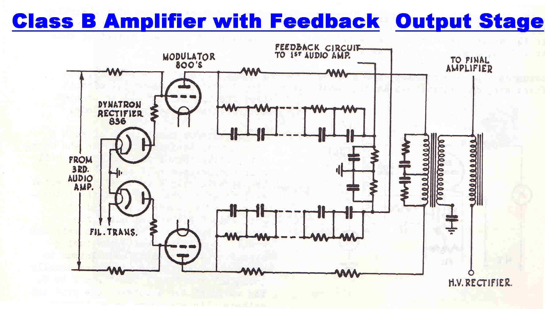
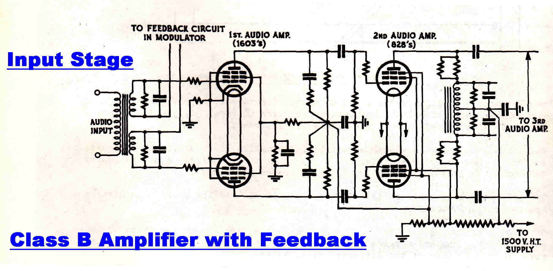 The circuit of a class B high power audio amplifier used for high level plate
modulation in an AM transmitter is shown on the right.
It is taken from a PMG training manual and is typical of the type used in most high level
modulated transmitters.
It is noted that the symmetrical feedback loops cover all amplifier stages and would therefore
seem to violate the principle described above.
This is not so, for only one side of the output stage is active at one time except for a small
crossover region.
The amplifier really consists of two independent amplifiers: one for the positive cycle and one
for the negative cycle.
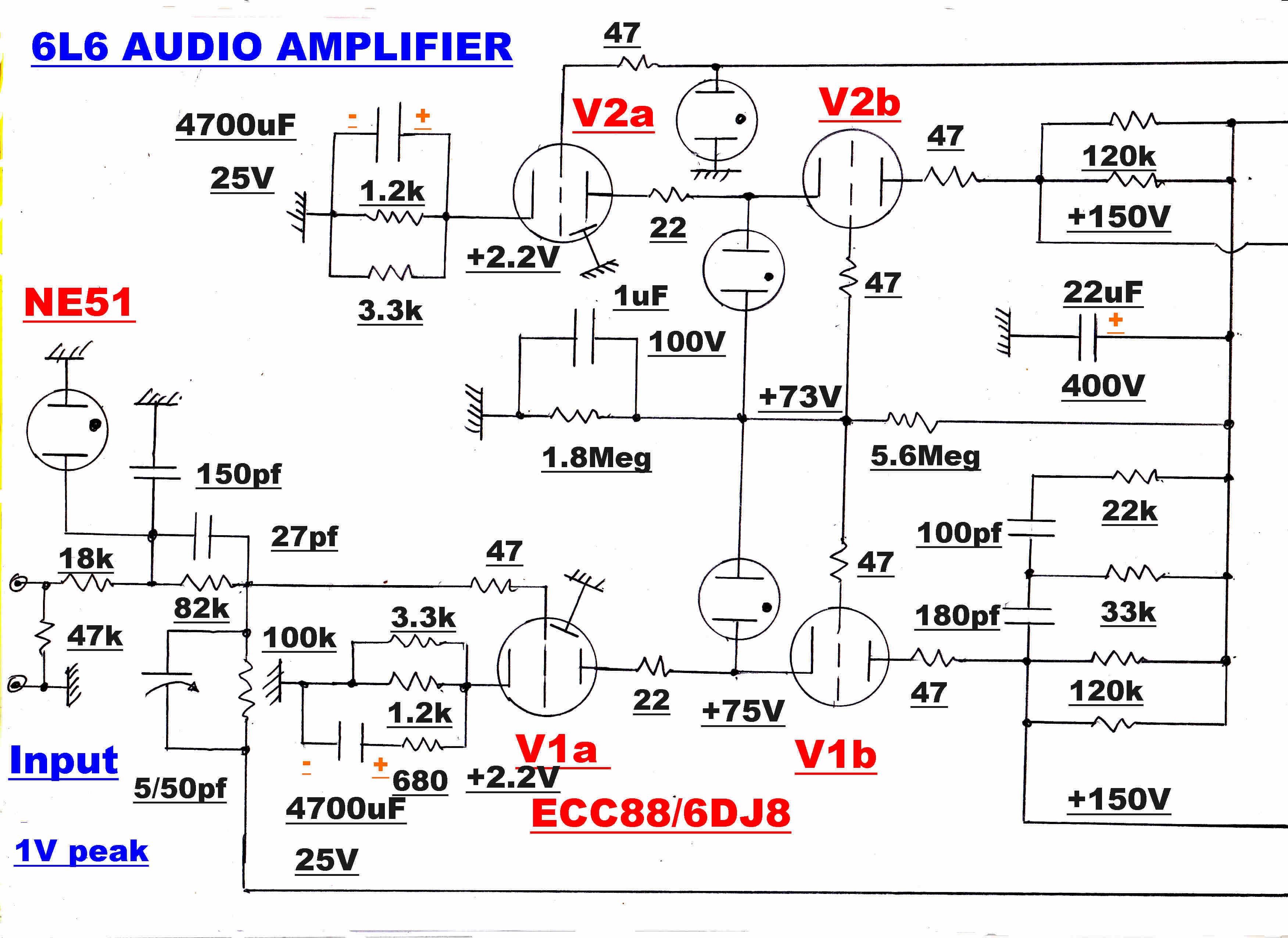
The input stage consists of two frame grid triodes (V1a,V1b) connected
in cascode.
This gives a low input capacity and a high output resistance.
A two terminal R-C network across the 60k load of the cascode tailors the open loop
high frequency response to allow a high degree of feedback with stability.
The cathode follower (V3b) gives a low output impedance to drive an R-C network which
tailors the low frequency response for stability in the main feedback loop.
The phase splitter consists of a unity gain operational amplifier.
Because of the high forward gain ( >> 200 ) the phase splitter has a high
bandwidth and very low drift over time.
The operational amplifier is the cascode ( V2a, V2b ) and the cathode
follower ( V3b ).
A feedback network around the output transformer splits the feedback into
a low and high frequency path.
The current drive to the primary of the output transformer results in the
following transfer functions:-
[1] At high frequencies:-
(a)The stray capacity across the primary produces a pole which gives
an ultimate slope of 6db/octave and a phase change of -90 degrees.
(b)The primary - secondary leakage inductance produces another pole
with the same result.
[2] At low frequencies:-
The primary inductance and reflected resistive load produce
a pole which gives an ultimate slope of 6db/octave and a phase change
of +90 degrees.
The extra pole appearing on the transformer secondary output at high
frequencies ( due to leakage reactance ) limits the overall feedback.
One of the most fundamental rules in the use of feedback is the following:-
Feedback must come from the output, not from some variable related to it.
The network is designed to take feedback from the secondary (output) over
the audio band up to 37.4KHz. and, above that, from the primary.
If the transformer is ideal, the network has a flat response.
The 6V6 amplifier used tubes current in 1938. Many of these are now in short supply.
The tubes in the 6L6 amplifier are all in current production, althouigh the 6L6 and the
ECC82/12AU7 could hardly be called "modern".
The 6L6 was designed by Otto Schade of RCA in 1936, although its genesis was not in the USA,
but in the UK.
Beam Power Tubes by Otto Schade IRE Feb. 1938 pp 320-364
Philips suppressed the secondary emission from the plate of a tetrode by
a potential minimum produced by a suppressor grid at cathode potential.
J.Owen Harries in the UK realised that a potential minimum would be produced by space charge
if the screen - plate distance was increased.
Cabot Bull and Sidney Rodda of EMI made further improvements including the introduction
of beam forming plates.
Production difficulties initially prevented the tube from going into production in the UK.
Puzzle : The detail design of this amplifier shows that the
distortion and response depend entirely on the circuit design
NOT the vacuum tube.
Yet advertising describes some 6L6 tubes as having "smooth"lows.
This seems to be against all the laws of Physics, but may herald
the start of a new religion.
The transit time of an electron in a 6L6 is of the order of a
nanosecond: far too fast to have any effect at audio frequencies.
There is a subtle effect at slow speeds: far too slow to have
any effect at audio frequencies:-
A voltage step applied to the grid of a tube produces a step
in plate current. This drops back by about 3% in tenths of a second.
Electrolysis occurs in the cathode, the emission drops,
the potential minimum near the cathode retreats towards the cathode and
the plate current decreases.
Direct coupled tube pulse amplifiers have slow speed networks to equalise the effect.
The ECC82 low mu double triode has been a workhorse since the late forties.
The ECC88 is a high slope medium mu frame grid tube.
The very small grid cathode spacing in frame grid tubes causes breakdown problems
- especially during warm up.
In the absence of cathode emission, an estimate of the electric field strength, E,
at the cathode is given by:-
E = Vgk/dgk
The stretched grid wire has a very small diameter, and so the grid surface has a small
radius of curvature - greatly increasing the field strength E.
Large grid cathode voltages probably start field emission at the surface of the grid.
The discharge then goes on to destroy the cathode.
Very large voltages can occur between grid and cathode during warm up before full
cathode emission is reached.
Small neon tubes across critical points limit the voltage to the striking voltage
of the neon.
The added parallel capacity is very small ( 0.3 to 0.4 pf ) and has negligible effect
with the neon dormant.
The input is also protected, since it may be driven from a vacuum tube preamplifier
which can produce very large voltage transients on its output during warmup.
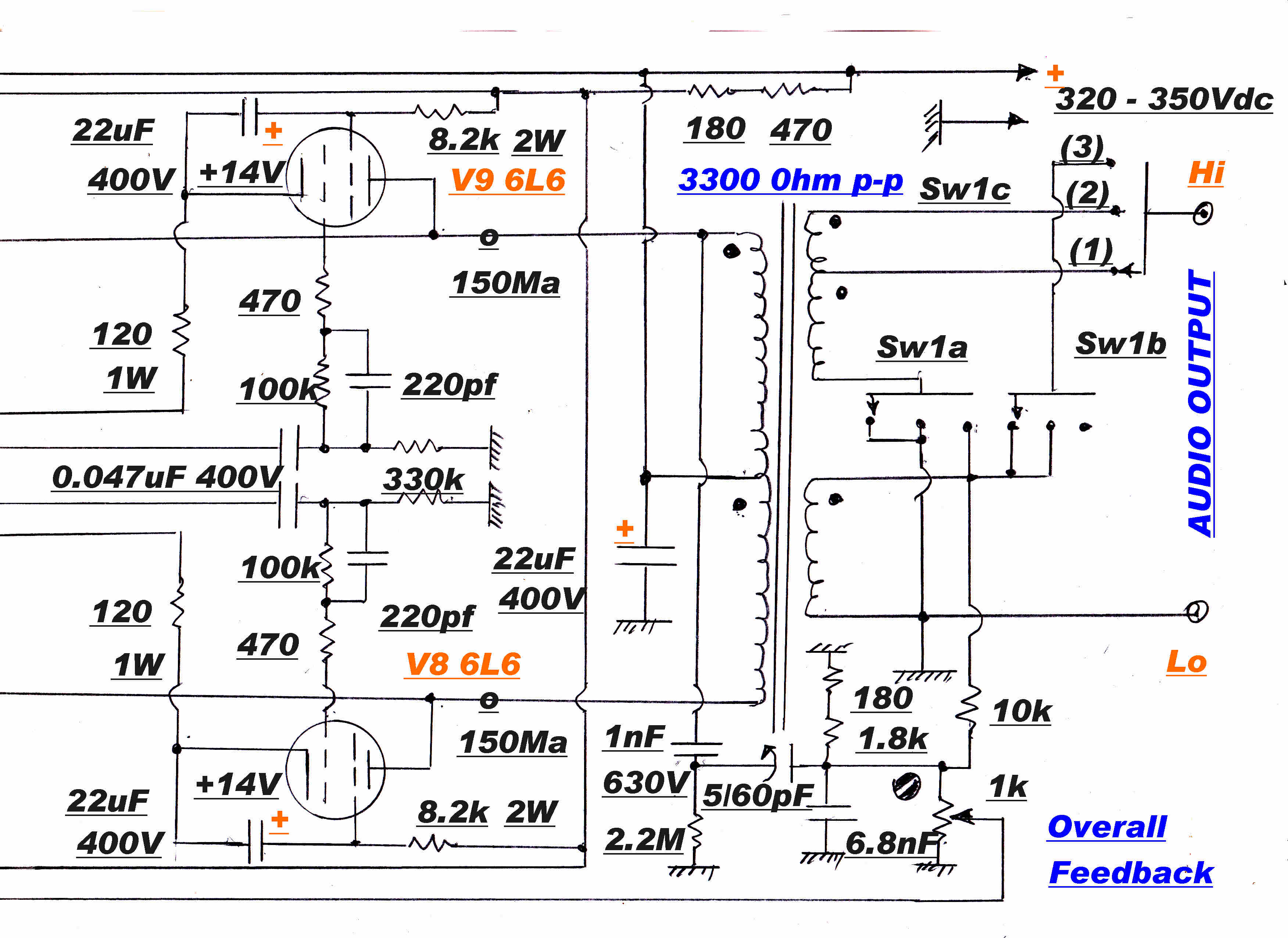
For an expanded circuit diagram click HERE
|
|
|
|
|
Note: |
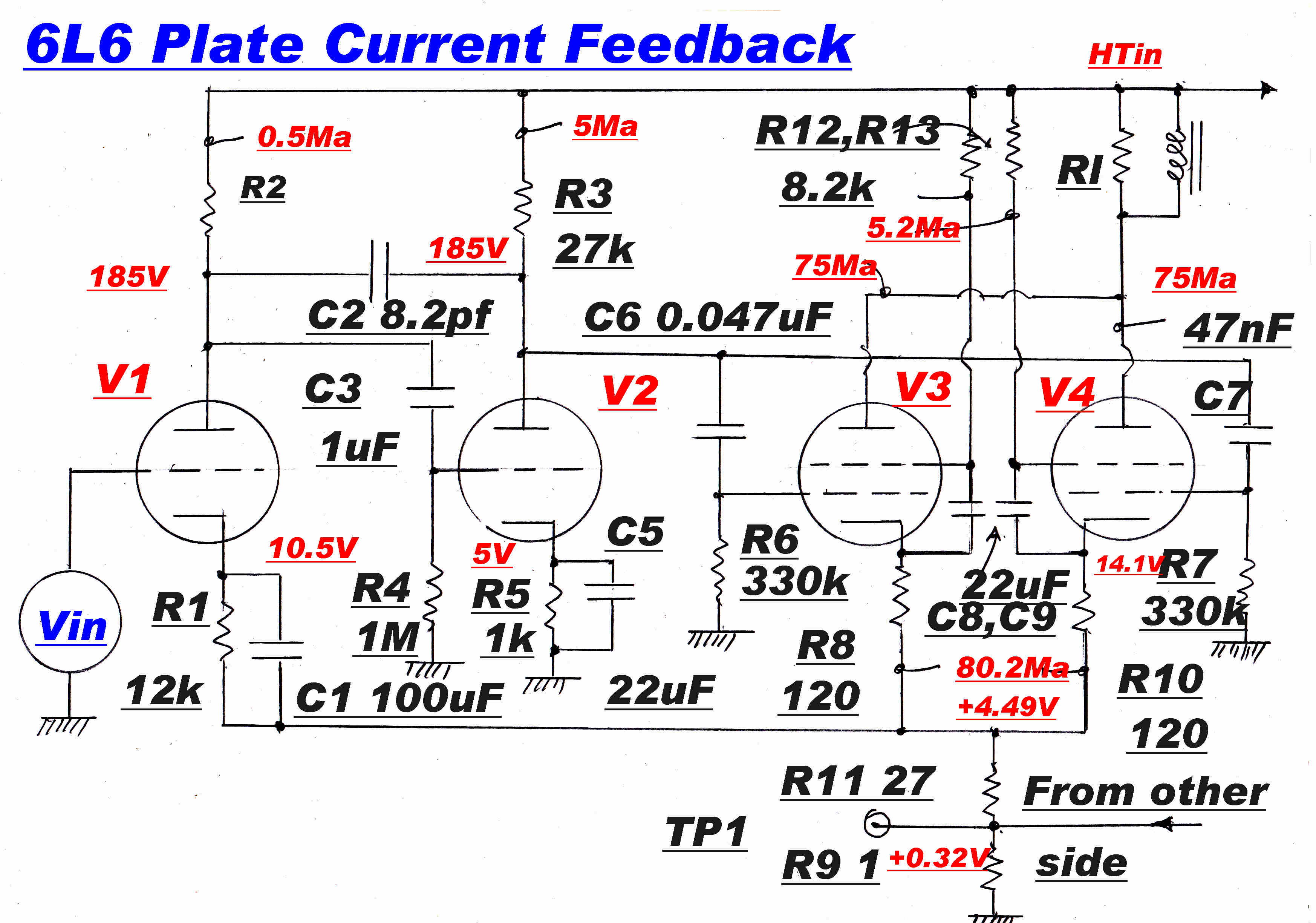
 The only convenient point to sense current is the cathode of the 6L6.
The 6L6 cathode current is the sum of the plate and screen current.
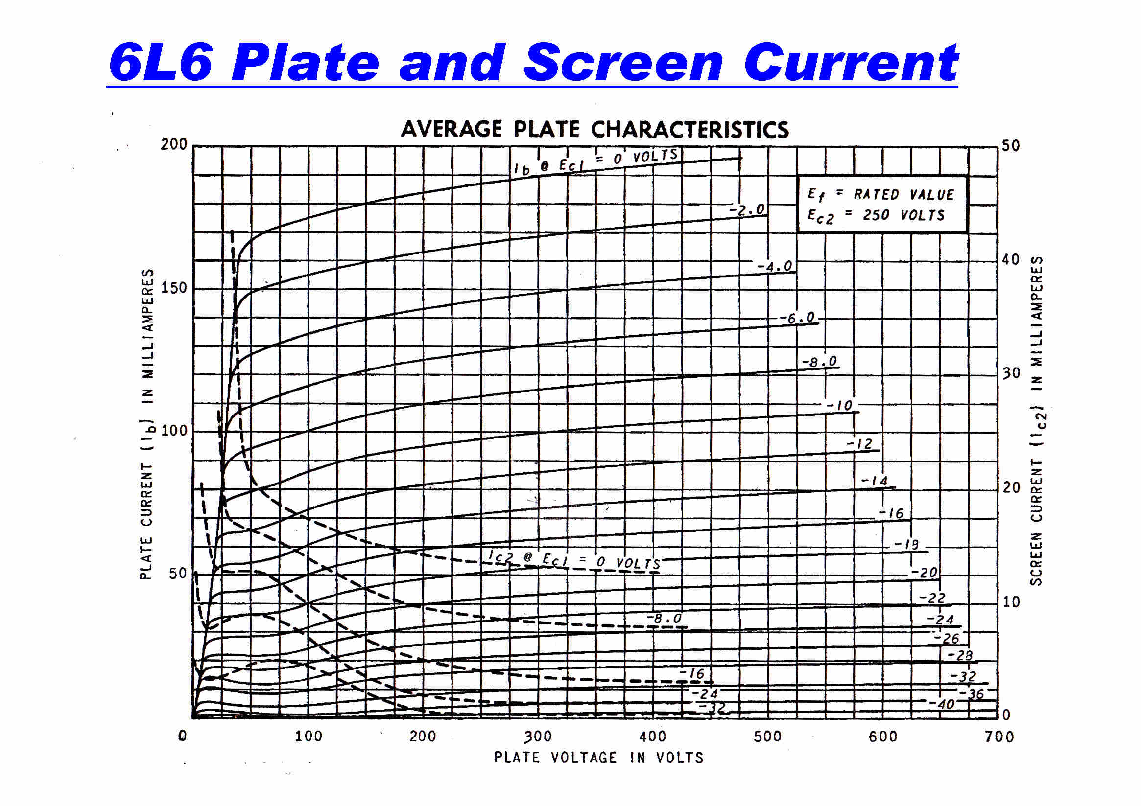
The plate - screen characteristics of the 6L6 are shown opposite and indicate that:-
[1] The ratio of screen to plate current is constant for high plate voltages.
[2] As the plate voltage drops below the screen voltage, the screen current kicks up in
a highly non-linear manner, so the unmodified cathode current can no longer be used for feedback.
The plate current is the signal of interest.
At signal frequencies the screen current must be subtracted from the cathode current to get
the plate current.
The screen current is shunted through a capacitor which has a much
lower impedance over the audio band than the screen dropping resistor.
The inclusion of a screen dropping resistor modifies the behaviour of the output stage
when operating at full power output and during overload conditions.
At very high prolonged power outputs the average screen current increases and the DC screen
voltage drops reducing the power output, and protecting the 6L6 from excessive
screen dissipation and failure.
For a normal audio signal the peaks have a small duty ratio and there is no limiting of peak power.
Amplifiers with the screens connected directly to high tension are prone to failure under
prolonged overloads.
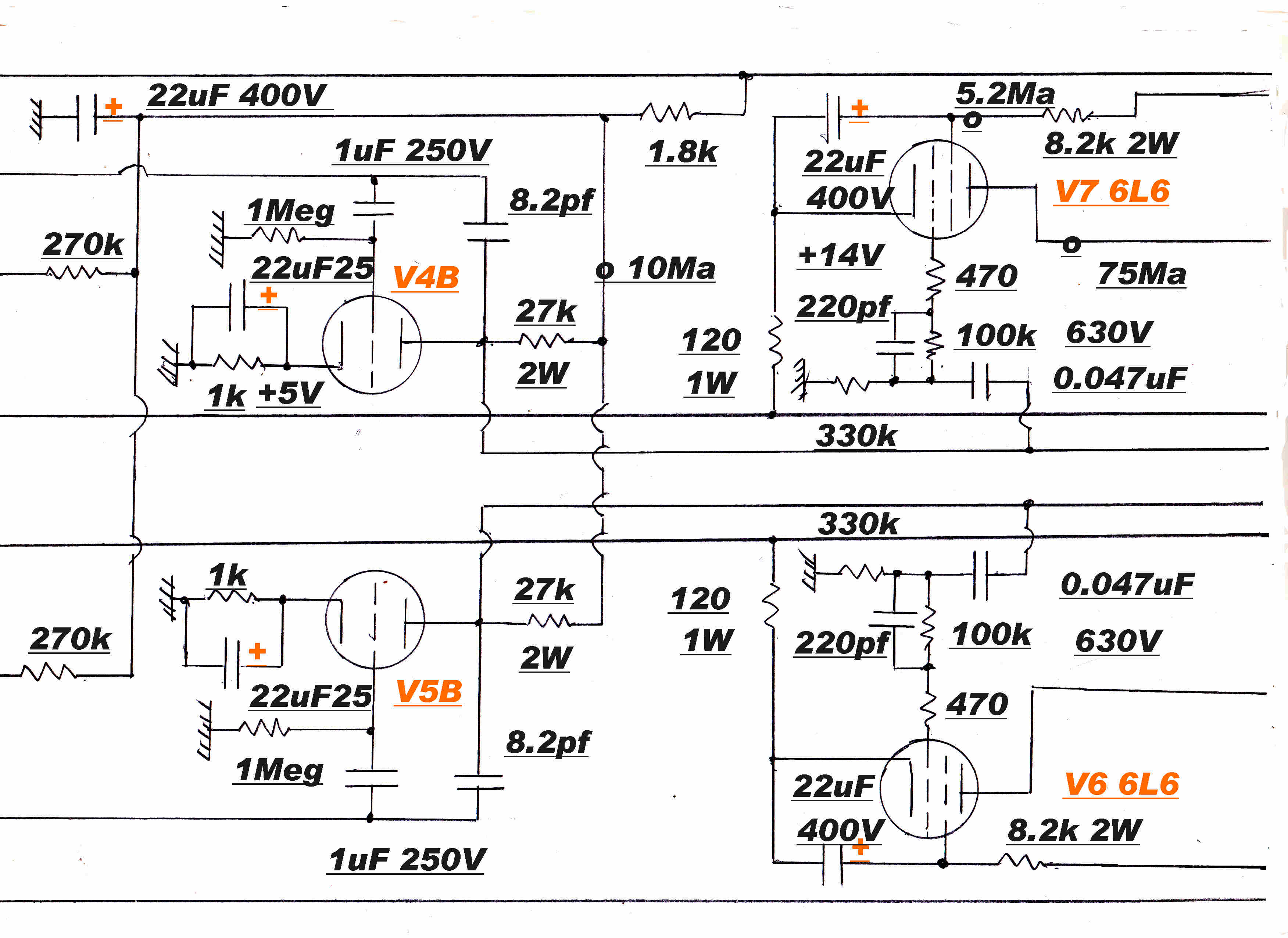
The 22uF screen bypass capacitors are returned directly to the cathodes, so the current flowing through the cathode bias resistor is the plate current. This is true over the working frequency range of the amplifier.
In the 6V6 amplifier, the screen capacitor current was sensed by a shunt and subtracted from the total cathode current in a low level stage.
Each 6L6 has its own screen, grid and cathode circuit.
Trouble with any tube is isolated and easily diagnosed.
The individual screen and cathode resistors provide DC stabilisation of the tube
operating point.
The current in each 6L6 must be summed in order to provide a feedback reference.
This implies a common resistor and a compromise in the isolation beween the two output tubes.
The common resistor must be large enough to generate the required amplitude for feedback,
but small enough to allow relatively independent operation of each tube.
The common resistor is 27 ohms and a further cathode resistor of 120 ohms is added
for each tube.
The removal or failure of one tube then does not produce excessive dissipation
in the other tube.
The total cathode current from all four 6L6s goes to ground through a common 1 ohm
resistor.
If the push pull stage is balanced, no signal will be developed across this
resistor. This can be used for the initial set-up. The internal feedback loops
maintain freedom from drift over long periods.
The voltage produced by the plate current across the 27 ohm resistor is fed back
directly into the cathode of the input ECC82 triode V1.
The 4.49 volt DC voltage acts as bias on V1. This is not desirable, since it is
generated by the output tubes. Any bias should be generated by the plate current of
V1 to give degeneration and stabilisation of the tube operating point.
AC coupling through a large capacitor would remove this effect, but make the low frequency
feedback stabilisation of the current loop more difficult.
Another solution is to choose an operating point for V1 which requires a bias
much greater than 4.49V, so the bulk of the bias can be produced with a cathode
bias resistor.
The choice of a low mu triode, together with a low plate current of 0.5 Ma, requires
a bias of 10.5 volts - allowing 6 volts of self bias and significant DC degeneration.
The distortion in both triode stages is small compared with distortion in the output stage.
No local feedback is required in these stages, so both cathode resistors are bypassed to
give maximum gain in the current loop.
The unbypassed cathode resistor in the 6L6s requires about twice the drive from
the 12AU7, and so increases the distortion in the driver.This is of opposite sign to that
in the output stage and so tends to cancel it - something for nothing!
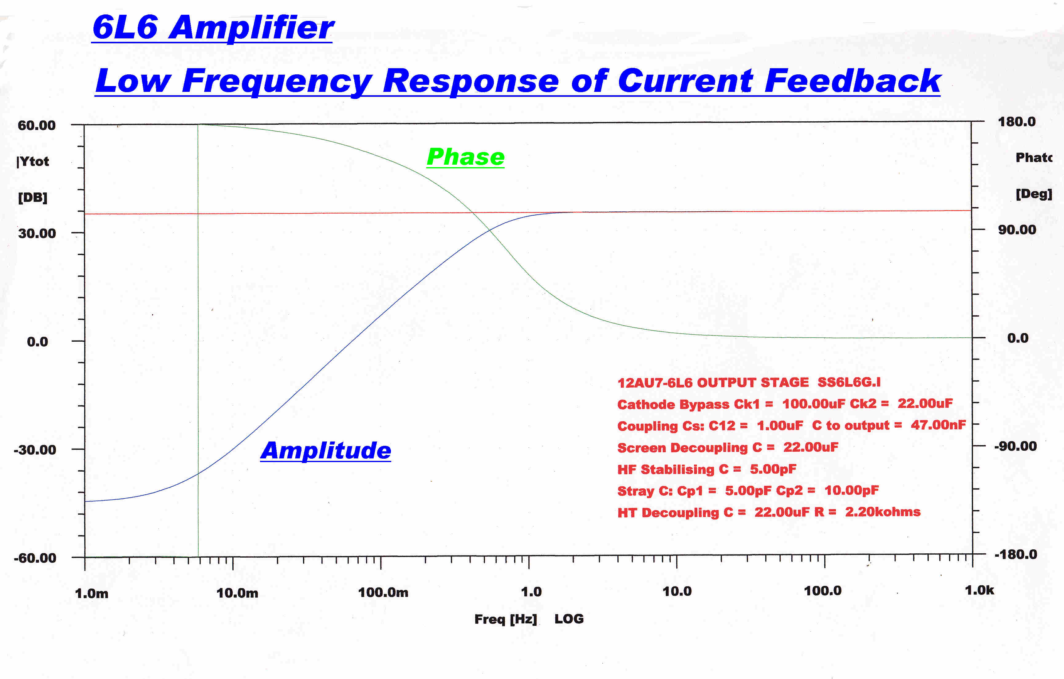 The low frequency response of the current feedback loop is shown
opposite.
The turnover frequency is lower than 1Hz. This is below the active frequency range of the
main overall loop, and so does not limit the degree of feedback in this loop.
In order to stabilise the low frequency response of the current loop, one of the
poles lying on the real axis in the forward path must have a much smaller time constant
( higher frequency ) than the others.
This pole is produced by the coupling capacitors and grid leak resistors of
the 6L6 output stage and gives a turnover frequency of about 10Hz.
It is important to keep this frequency as high as possible for the following reasons:-
(1) During overload the 6L6 grid current rapidly charges the coupling capacitor
and the resulting change in bias can paralyse the amplifier.
Paralysis time decreases with the coupling time constant.
(2) The 6L6 grid coupling capacitor should be a high quality 630 volt capacitor,
so smaller values of capacitance reduce the physical size and associated stray
capacity to earth.
(3) Grid current flowing through the grid leak resistor produces a spurious
grid bias. The resistance from the grid to earth should therefore be as small as possible.
For tubes in good condition the effect is small but highly variable.
Electrons accelerated through more than about 20 volts ionise the residual gas left in the tube.
The positive ions then migrate to the negative grid.
+20mV to 100mV - 10nA to 50nA - would be typical for a tube in good condition.
Negative grid current can also be caused by thermionic emission from the grid.
If the surface of the grid is contaminated during manufacture, the work function can
be lowered to produce thermionic electron emission. The effect can be regenerative and lead to
run away plate current and destruction of the tube.
Emission lowers the grid voltage and increases the plate current : so giving higher
plate dissipation and an increase in temperature leading to a higher grid temperature
and more emission - runaway.
The time constant associated with this effect is long and usually occurs minutes after
the amplifier is switched on.
The 6L6 cathode and screen resistors provide DC degeneration and help suppress the effect.
To sum up:-
Low frequency response dictates a high grid resistance to earth and cathode current stability
pushes in the other direction.
If trouble is encountered with tubes of a given manufacture, the 100K grid limiting resistors
can be reduced to 47K to mitigate the effect.
EXPERIENCE WITH 6L6 GRID CURRENT
No trouble has been experienced with old 6L6s of US and UK manufacture.
The total grid resistance to earth in this amplifier is 430K ohms and this is OK with these tubes with grid current
measured in nanoamps.
Many tubes of Russian origin tend to have larger grid currents measured in microamps giving rise to a potential runaway situstion.
In this amplifier the grid resistance to earth can be lowered with negligible change in performance.
[A] Reduce the grid leak R from 330K to 100K
[B] Reduce the blocking resistor across the 220pf condenser from 100K to 22K.
The 6L6 grid resistance to earth is changed from 430K ohms to 122Kohms.
The 12AU7 triode driver acts as a current generator of Gm = 1.6Ma/V shunted by an output impedance
of 9.69Kohms, so it is easy to calculate the loaded gain.
Initial gain = 10.93
Reduced gain = 9.98 - making little difference to the current loop.
The grid current appears to be thermionic grid emission and so is very sensitive to tube temperature.
This can be lowered by increasibg the common screen dropping resistor.
As shown, this consists of an 180 ohm R in series with a 470 ohm R. Replacing the 180 ohm with a 1.5K 2W resistor
has a dramatic effect in lowering the grid current.
The power output is slightly reduced, but the gain in tube operating point stability is well worth it.
To maintain the same low frequency current loop transfer function, the coupling capacitor must be increased to 0.15uF ( 3.3x 0.047 ).

The AC load on the 12AU7 driver has been reduced from (330/2) K to (100/2) K. This reduces the peak output swing
obtainable from the driver.
The peak output swing can be estimated by drawing the new AC load line on the stage as shown opposite.
Since a peak output swing of about 25 volts is required, the drive is adequate.
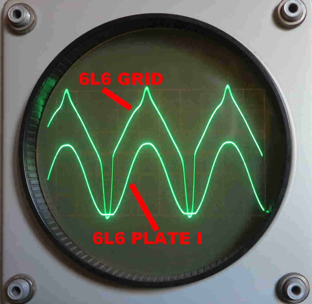 The peak transient voltages during overload are greatly increased in
an amplifier with feedback.
It was noted above that a short R-C time constant of the 6L6 grid coupling
reduces paralysis time.
In this amplifier the effect is greatly reduced by limiting the long term
6L6 grid current by a 100k/220pF network in series with the grid.
This is not shown in the simplified circuit, but appears in the complete
circuit.
When the 6L6 grid is driven positive, the grid cathode diode clamps
the grid voltage at approximately 0 volts and the excess voltage appears across
the 100k ohm buffer - charging up the 220pF capacitor.
The recovery time after overload is now ( 220 10-12 x 100k )
= 22uS compared with ( 47 10-9 x 330k ) = 15.5mS - a reduction
by a factor of 705.
The network has virtually no effect on amplifier performance under normal
operating conditions.
The low frequency impedance looking into the 6L6 grid is so high that
the 100k series resistor has no effect.
At high frequencies the tube input capacity forms a capacitive
divider with the 220pF capacitor.
The tube input capacity is 10pF, but this is reduced by degeneration
in the cathode.
The effective cathode resistance is : 120 + 2x27 ohms shunted by
the screen resistance of 8.2k = 170 ohms.
With cathode degeneration, the Gm and input capacity
Cin are reduced by the factor 1 + GmRk
Here Gm = 5.5 mA/V, so the Cin is reduced by
1.935 to 5.2pF.
The capacitive divider then attenuates the high frequencies by
a factor of 0.977. The turn over frequency is given by
fc = 1/(2x Π x 225.2 10-12 x 105 )
= 7.06KHz.
This small effect is completely masked by the very large degree of
feedback over the 6L6 output stage (>40db).
The large grid drive under overload is illustrated in the oscillogram
taken with only the internal current feedback loop active.
The positive going pip on the grid drive is to compensate for loss of gain
as low plate voltage traverses the knee of the plate curve.
The long extended negative pip overcomes tfhe loss of gain at low plate currents.
Every centimetre of conductor has its own little pico-Farad and
nano-Henry, and frequently significant mutual inductance .
These may inadvertently take on the topology of a VHF/UHF oscillator
around an active element.
If the gain is sufficient, oscillations build up exponentially
until non-linearity in the active element limits their amplitude.
The operating point is changed and, with it, the behaviour at signal
frequencies.
The output stages of vacuum tube audio amplifiers typically develop
parasitics from about 50MHz to about 100MHz. Usually the tubes are
driven into grid current and large biases are built up across the grid
leak resistor - reducing the plate current.
The name originated in transmitter design in the early tewnties.
Then grid and anode leads were long. The resulting spurious oscillation
reduced the transmitter output, so they appeared to exist on the lost power
and so the "parasitic" existence.
They are suppressed first by careful layout, and then by introducing
resistive losses which cripple the oscillation but leave operation at the
signal frequency untouched.
With vacuum tubes, the first line of defence is usually a small resistor
soldered directly onto the grid tag. This forms a low pass filter with
the grid input capacity, and introduces losses into any inductance
in the grid circuit. In this amplifier the grid suppressors are 470 ohms.
For an input capacity of, say, 10pF this gives a cutoff frequency of
62.55MHz -- well outside the working frequency range, but at the bottom
of the parasitic frequency range.
Small resistors can be introduced into the plate circuit. The large plate
current in power output stages prohibits this. A small inductor is then
added in parallel with the resistor - usually on the resistor's body.
Modern practice is to use a few turns on a ferrite toroid with large
core losses at the parasitic frequency.
Frame grid tubes such as the ECC88 are particularly prone to parasitics.
Finally it should be mentioned that one particulsr circuit configuration
has a great propensity for spurious oscillation - the cathode follower.
The cathode follower has a negative input conductance for capacitive loads.
This cancels out the losses in any phantom tuned circuit in the grid -
usually resulting in violent VHF oscillation.
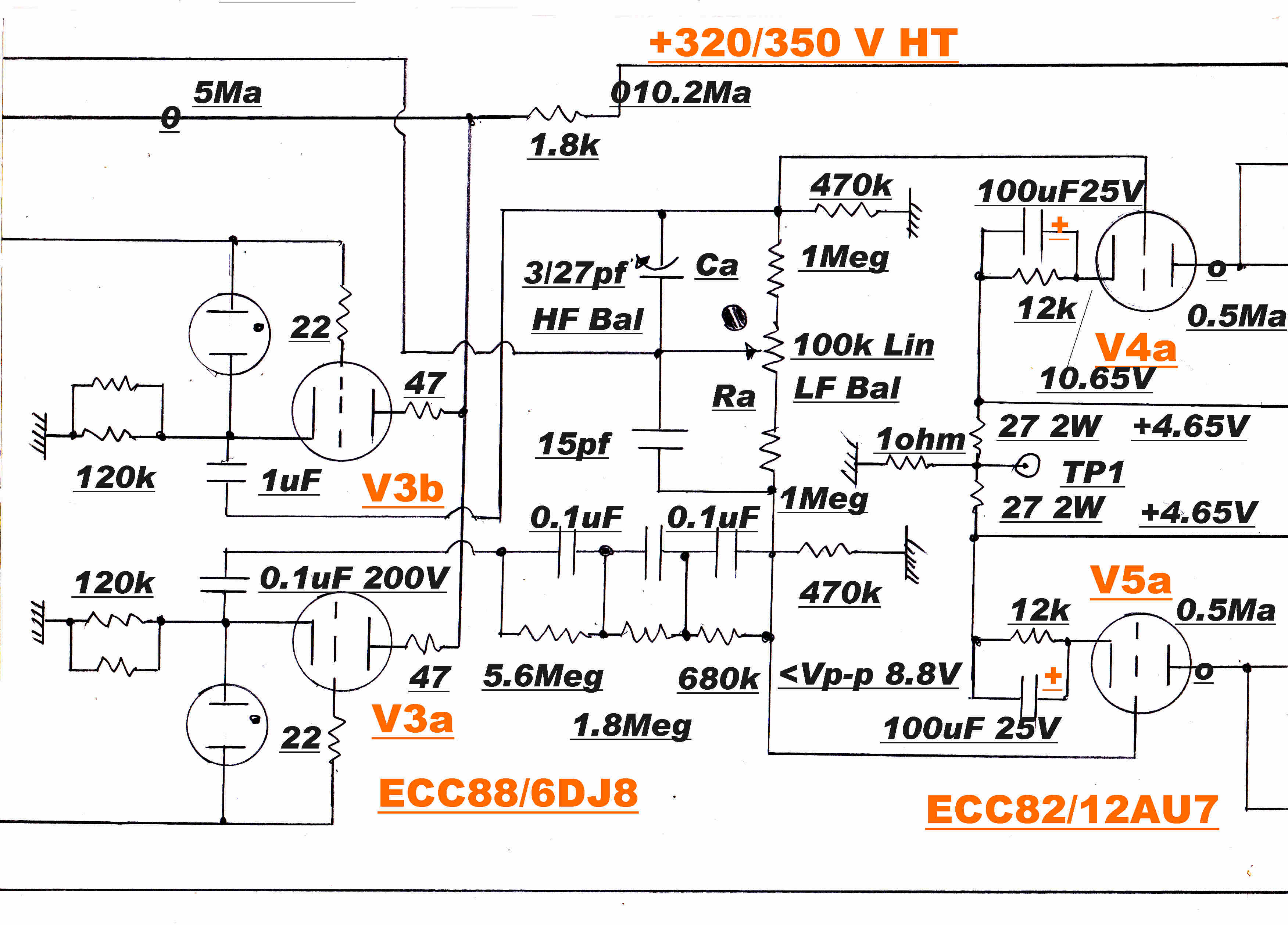
Note that the cathode followers ( V3a, V3b )( main circuit) have
a 22 ohm suppressor in the grid and a 47 ohm suppressor in the plate.
It is convenient to break up the 6L6 plate current feedback loop into
three sections:-
(1) The 6L6s ( V3, V4) and their cathode load (R8, R10, R11 ).
The 6L6s on one side can be grouped together and treated as a tetrode
cathode follower with an effective Gmof 2x5.5Ma/V = 11Ma/V.
Since the screen is bypassed to the cathode, the tubes behave as tetrodes and
have a very high plate resistance ( Rp ) and
amplification factor ( μ).
Using Thevenin, a cathode follower has an equivalent voltage generator of
[ μ/( 1 + μ )]Vin
and an output resistance of
[ μ/( 1 + μ )]/Gm
Since μ >> 1 , [ μ/( 1 + μ )] ≈ 1 and the output from the cathode
can be considered as Vin behind a a resistance (1/Gm) =
1/11x10-3 = 90.9 ohms.
The total cathode load is (120/2 +27 ) = 87 ohms, so the signal at the cathode
of the 6L6s (Vk) is given by:-
Vk = Vin x[ 87/(87 +90.9) ] = 0.489Vin
The signal appearing across the 27 ohm resistor is then 0.1518Vin
Because of the low impedance the bandwidth is large and well outside the active range
of the feedback loop.
(2) The Input Stage V2
The input stage is an ECC82 low μ triode operating under
the following conditions:-
Vp = 185V: Vg = -10.7V: Ip = 0.5Ma
Gm = 0.2Ma/V: μ = 12.5 : Rp = 62.5k
Cpg = 1.5pF: Cgk = 1.6pF : Cpk = 0.5pF.
The feedback signal from the 27 ohm sensing resistor is injected directly
into the cathode. The output impedance of the phase splitter is low and
prevents any of this signal appearing on the grid.
The stage therefore operates as a grounded grid stage.
The stage acts as a current generator injecting current into the grid of V2.
For a grounded grid stage the effective Gm (Gme) is given by:-
Gme = Gm
[( 1 + μ )/μ][ 1/( 1 + RL/RP )]
where RP is the plate resistance and
RL is the total load (270K//1Meg = 212.6K)
So Gme = 4.91x10⁻⁵ A/V
Voltage gain = GmeRL = 10.4
(3) The Output Driver Stage V3
The driver stage is an ECC82 low μ triode operating under
the following conditions:-
Vp = 185V: Vg = -5V: Ip = 5Ma
Gm = 1.6Ma/V: μ = 15.5 : Rp = 9.69k
Cpg = 1.5pF: Cgk = 1.6pF : Cpk = 0.5pF.
The resistive load on the stage is: (27k//330k//330k)= 23.2k, so
the mid-frequency gain of the stage = 10.93.
The loop gain is then given by:
Aloop = 0.1518x10.4x10.9 = 17.2
The gain reduction Afb (feedback) in the current
loop is then given by:
Afb = 1/( 1 + Aloop ) = 18.2 --- (25.2db)
The reduction in gain Akr by the unbypassed
6L6 cathode resistor (87 ohm ) is given by:
Akr = 1/( 1 + GmRk )
Then Ark = 1/( 1 + 11x10-3x87 ) = 1/1.957 --- -5.83db
The total feedback over the 6L6 output tubes by the internal feedback
loops is then (25.2 + 5.8)db = 31db.
The driver stage determines the high frequency loop response.
The input capacity, together with the output capacity of V1, produces a
pole on the real axis. The input capacity is increased by Miller effect
and the added capacity Cm is given by:-
Cm = A x Cpg = 10.9 x 1.5pF = 16.4pF.
The output capacity, together with the 6L6 input capacity, produces
another pole on the real axis.
Analysis shows that the amount of feedback that
can be applied to such a system without overshooot and ringing
increases with the pole separation.
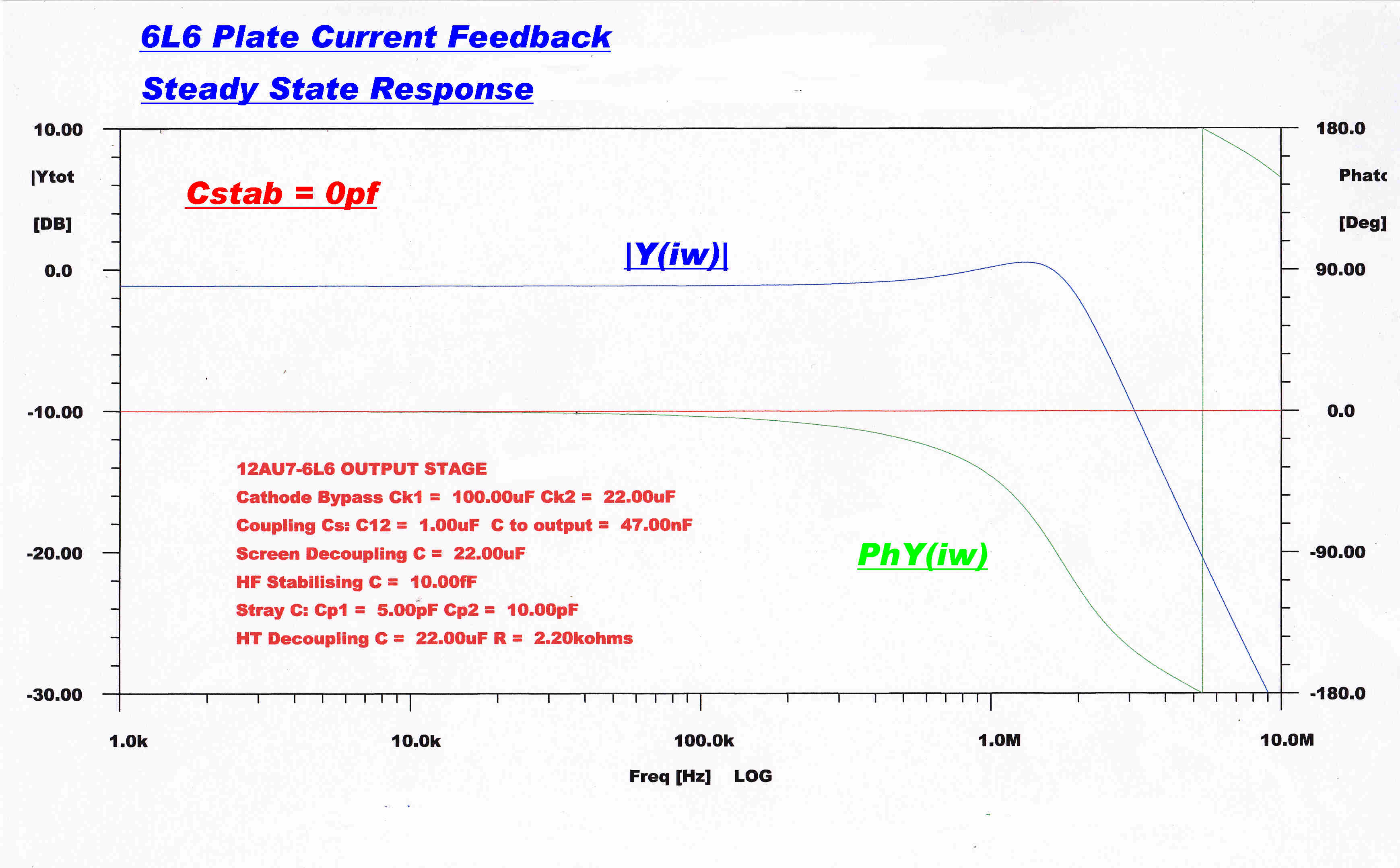
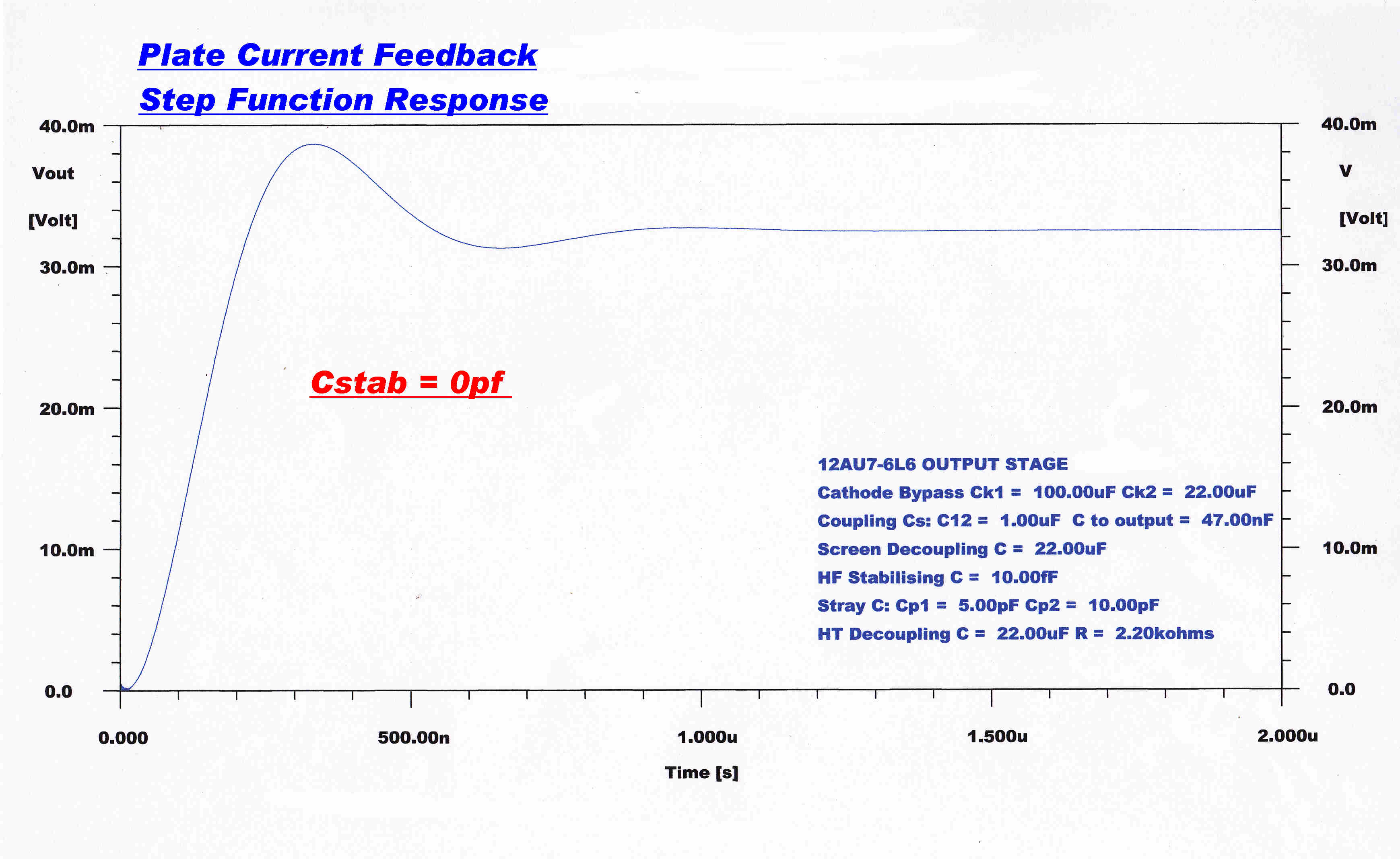
The steady state and transient response of the current loop
without stabilisatiion is shown below:-
|
|
|
HF Steady State Response :: Cfb = 0 pF |
Fast Step Response :: Cfb = 0 pF |
It is desirable to reduce the bandwidth of the current loop until it
just sits outside the range where it starts to interfere with the
stability of the main loop.
Lower bandwidths give greater freedom of layout and
improve dynamic stability.
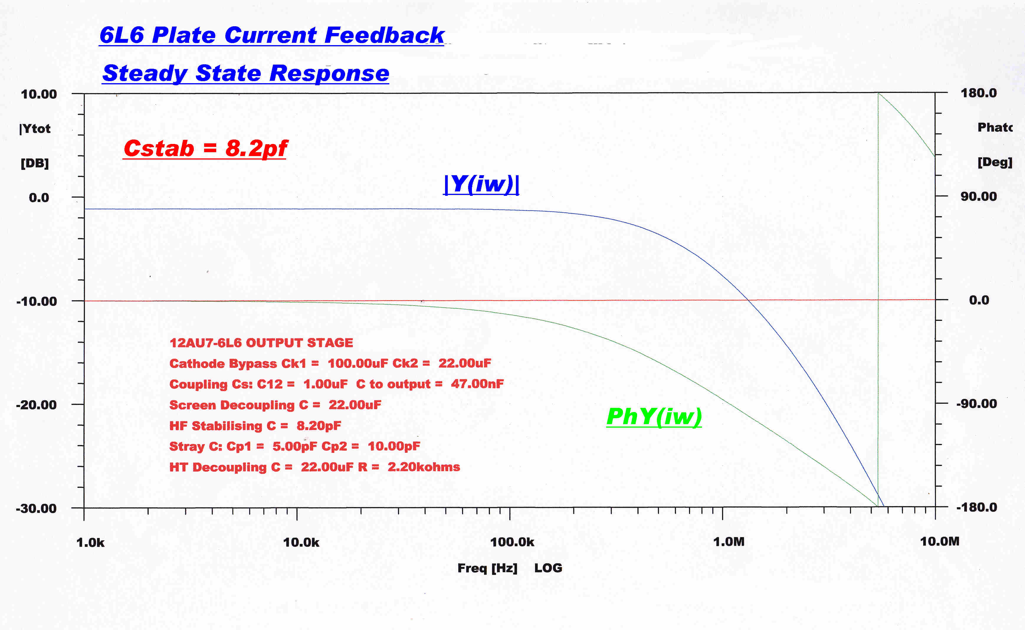
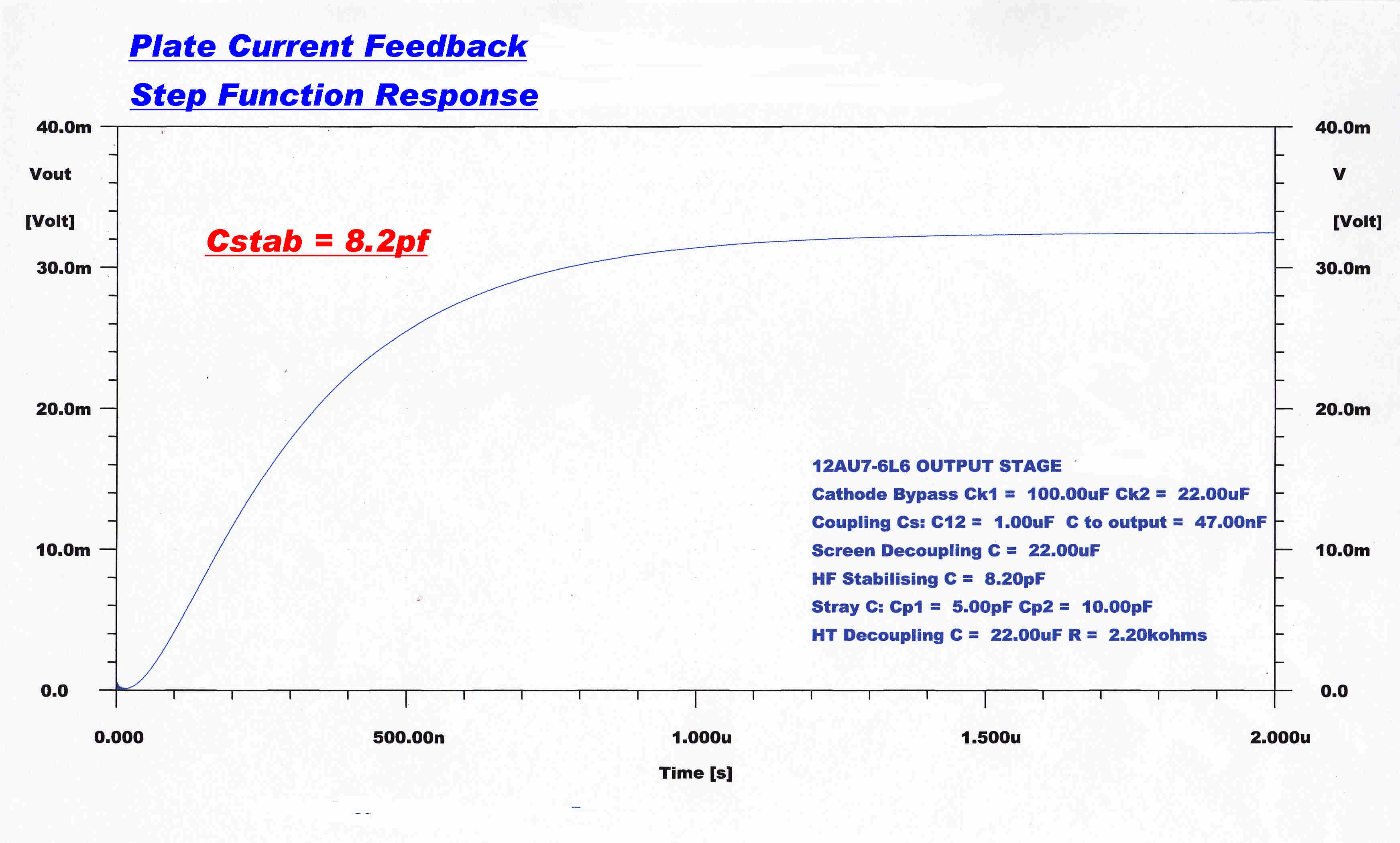
Increasing the Miller effect in V2 artificially with an external 8.2pF capacitor
shifts the input pole towards the origin - thus producing greater pole
spacing and stability.
Since the plate of V1 is at the same signal potential as the grid of V2,
the capacitor is connected between the plates of V1 and V2 to remove the
DC voltage across the capacitor.
The modified response is shown below:-
|
|
|
HF Steady State Response :: Cfb = 8.2 pF |
Fast Step Response :: Cfb = 8.2 pF |
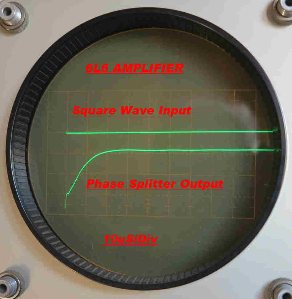
 It is claimed above that the response of the plate current feedback loop
has no significant effect on the response of the forward path of the amplifier.
The oscillogram on the right confirms this.
A 2KHz square wave is applied to the input of the amplifier with the main
feedback loop open.
The input R-C low pass filter and the HF stabilisation network produce
an output from the phase splitter shown on the bottom trace.
This is also the drive for the current feedback.
The plate current is shown on the top trace.
The two are identical.
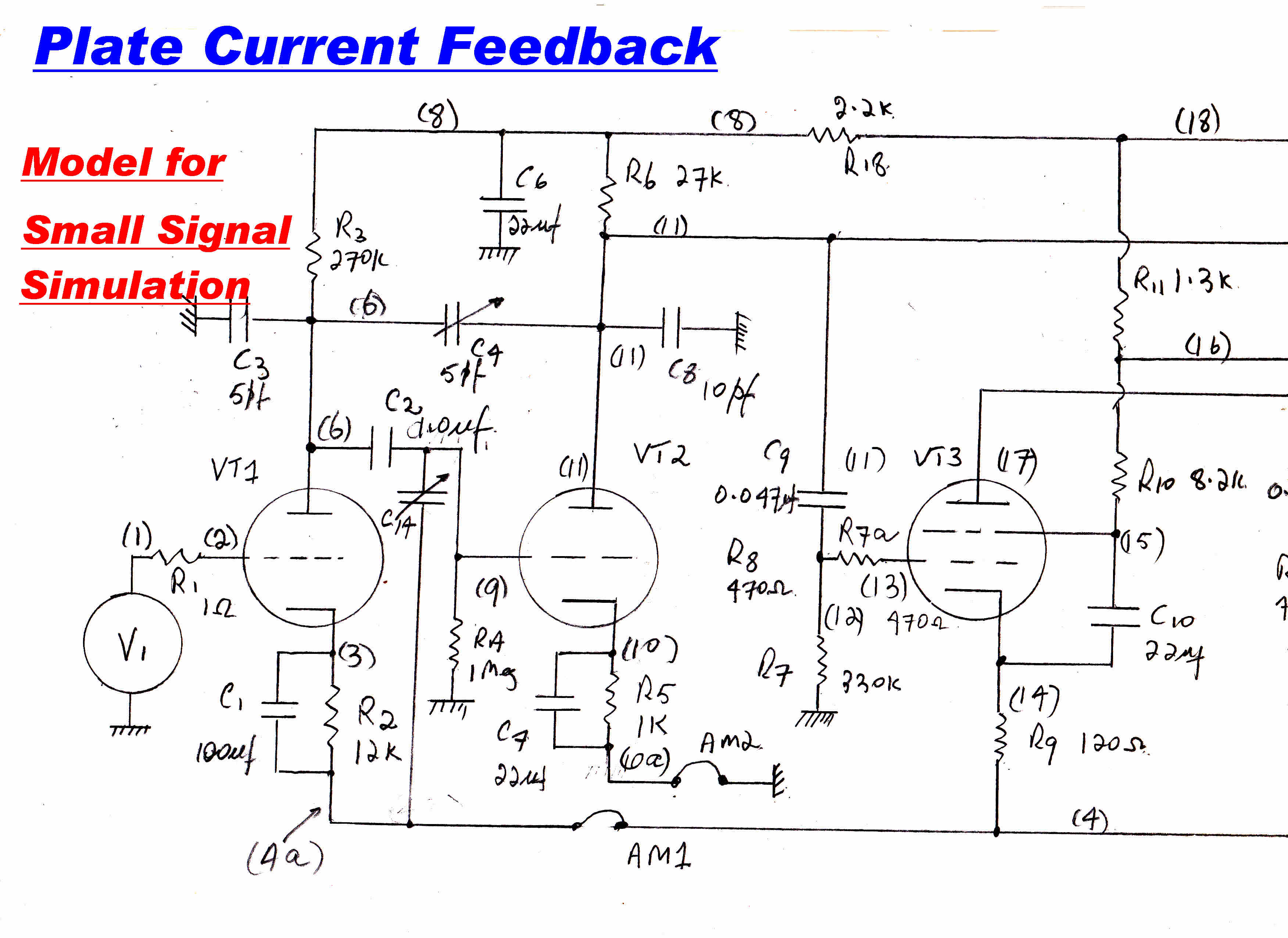
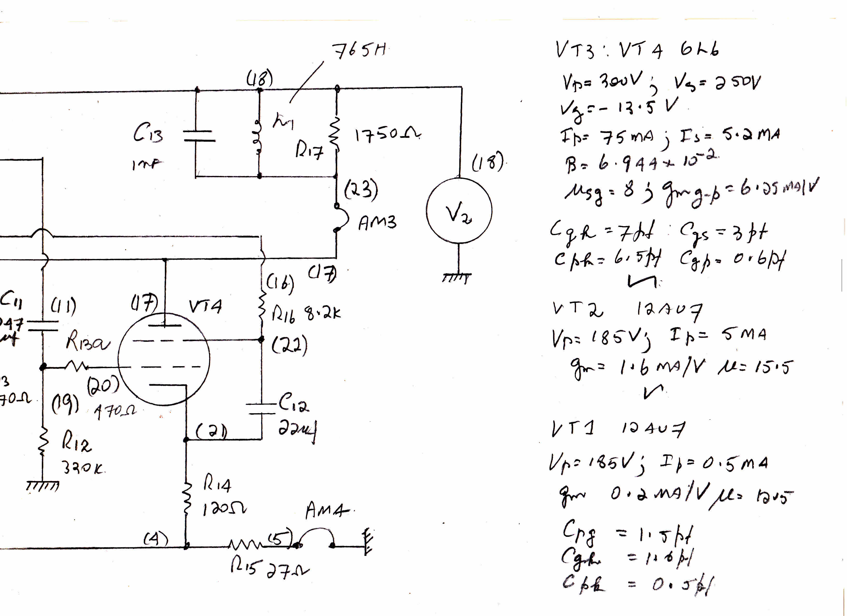
A sketch of the computer model for the plate current loop is shown below:-
|
|
Infrequently vacuum tube amplifiers, which are otherwise
stable, exhibit instability during warm up.
High frequency oscillation may alter the operating conditions
in one or more stages to cause a lockout, so the amplifier never reaches stability.
The mechanism of this behaviour must be understood before preventitive measures
can be taken.
The trouble in almost all cases can be traced to active element synthesis
of a stabilising network.
From the above diagram we see that:-
The HF stabilising network for the current loop is obtained by feedback via C4
around the active element VT2. If VT2 is inactive ( say during warm-up ), then there is
still a forward path between grid and plate via C4.
The transfer function of this path is very different from when VT2 is active and may
cause instability if VT1,Vt3,VT4 have become active.
Computer runs with the Gm of VT2 varied from zero to its nominal value
showed that current loop was free of instability under all conditions.
Another possible position for the stabilising capacitor is shown as C14.
Since the feedback line has a much lower impedance than the plate of VT2,
the effect should be minimised. Computer runs show that the stabilising effect of C14
was as expected.
Since C4 did not cause trouble and leads to more convenient wiring it was adopted.
The input stage consists of two triodes in cascode followed by a cathode follower.
The upper triode of the cascode operates grounded grid with a low impedance looking
into the cathode, so that the gain and Miller capacity of the bottom
triode is small, but usually not insignificant.
The input and output impedance are high, but the isolation between input and output
is not as complete as that found in a pentode. On the other hand, there is
no screen feed and decoupling to reduce the low frequency response.
The operating conditions for the two triodes in the cascode are the same:-
Vp = 75 volts: Vg = -2.2V: ip = 2.5Ma: Gm = 5Ma/V: μ = 33: Rp = 6.6K
Cgk = 3.3pF: Cgp = 1.4pF: Cpk = 2.5pF
The operating condition for the cathode follower triode:-
Vp = 150 volts: Vg = -4.8V: ip = 2.5Ma: Gm = 4.77Ma/V: μ = 33: Rp = 6.92K
Cgk = 3.3pF: Cgp = 1.4pF: Cpk = 2.5pF
If RL is the load on the cascode, the impedance Rin looking
into the top cathode is:-
Rin = ( RL + RP )/ ( μ + 1 )----(1)
OR:-
Rin =[ μ/(μ +1 ) ][ 1/GM
+ RL/μ ] -----(2)
Now μ/(μ +1 ) ≈ 1
So for low loads RL
Rin ≈ 1/GM
This is low, the voltage gain of the first stage low, and so the Miller
input capacity.
Norton's Theorem
If we represent the cascode stage by a current generator in parallel
with a resistance, some algebra will show that the GM of the
current generator is given by:-
GMNor = GM /
[ GM RK ( 1 + μ)/ μ
+ ( μ + 2 )/( μ + 1 ) ]
and the output resistance, Rout, is given by:-
Rout = [ ( μ + 1 ) 2RK
+ ( μ +2 )RP
where RK is an unbypassed resistor in the cathode of the
bottom tube of the cascode.
If RK = 0, that is the bias resistor is bypassed
with a large capacitor then:-
GMNor = GM [ (1 + μ )/(2 + μ) ]
Rout = ( μ + 2 )RP
Since μ >> 1 , to a good approximation, the GM
of the cascode is the same as that of the tubes and the output impedance
is high, μ times that of the tubes.
Thevenin's Theorem
If we represent the cathode folower by a voltage generator
VT behind an output resistance RT then:-
VT = Vin [ μ/( 1 + μ ) ]
RT = [ μ/( 1 + μ ) ] [ 1/GM ] ]
Since μ>> 1, we usually spproximate in design to:-
VT = Vin
RT = 1/GM
Numerical Values
Up to about 10KHz the load RL on the cascode is 60K
The cathode degeneration RK is 680//1200//3300 = 384 ohms so:-
GMNor = 1.664Ma/V
Rout = 674K
Cascode Voltage Gain = 91.7
Cathode Follower Voltage Gain = 0.967
Cathode Follower Output Impedance = 203 0hms
Overall Voltage Gain = 88.6
Low Pass R-C Input Filter
RF can enter the amplifier, especially if long leads
are used from the preamp.
It is prudent to reject the RF in a low pass R-C filter
right at the input.
Because of feedback, the grid of the input cascode may be
considered to be at earth potential.
The capacity to earth is then 177pF and the driving point impedance is:-
18k//82k = 14.76K to give a cutoff frequency of 112.5KHz.
The feedback signal is applied to the grid of the input cascode,V1a ,
via a compensated resistve divider ( 100k/82k ). Since the input end of the
18K resistor is usually driven from a low output impedance preamplifier,
it can be considered at earth potential for the feedback signal.
On removal of the input connection from the preamp, the 47K R
and 150pF C ensure that there is little change in the division ratio
and stability is maintained in the main feedback loop.
The neon protects the grid of V1a from excessive voltage during warm up
when using a vacuum tube preamp.
In this prototype amplifier tests required that the overall feedback loop be broken.
A 1K pot in the output network facilitates this. In a normal amplifier the pot can
be replaced by a 1K resistor.
These are passive R-C networks which modify the response of
the forward path so that more overall feedback can be applied with stability.
For networks which have all thir zeros in the left half plane, the phase response
is a unique function of amplitude response. They are called minimum phase networks.
If the attenuation is less than 6db/octave, then the phase change is less
than 90 degrees.
This means that we can get rid of gain without large destabilising phase changes.
The networks, then, have an attenuation rate less than 6db/octave between two
set frequencies and are known as shelf networks.
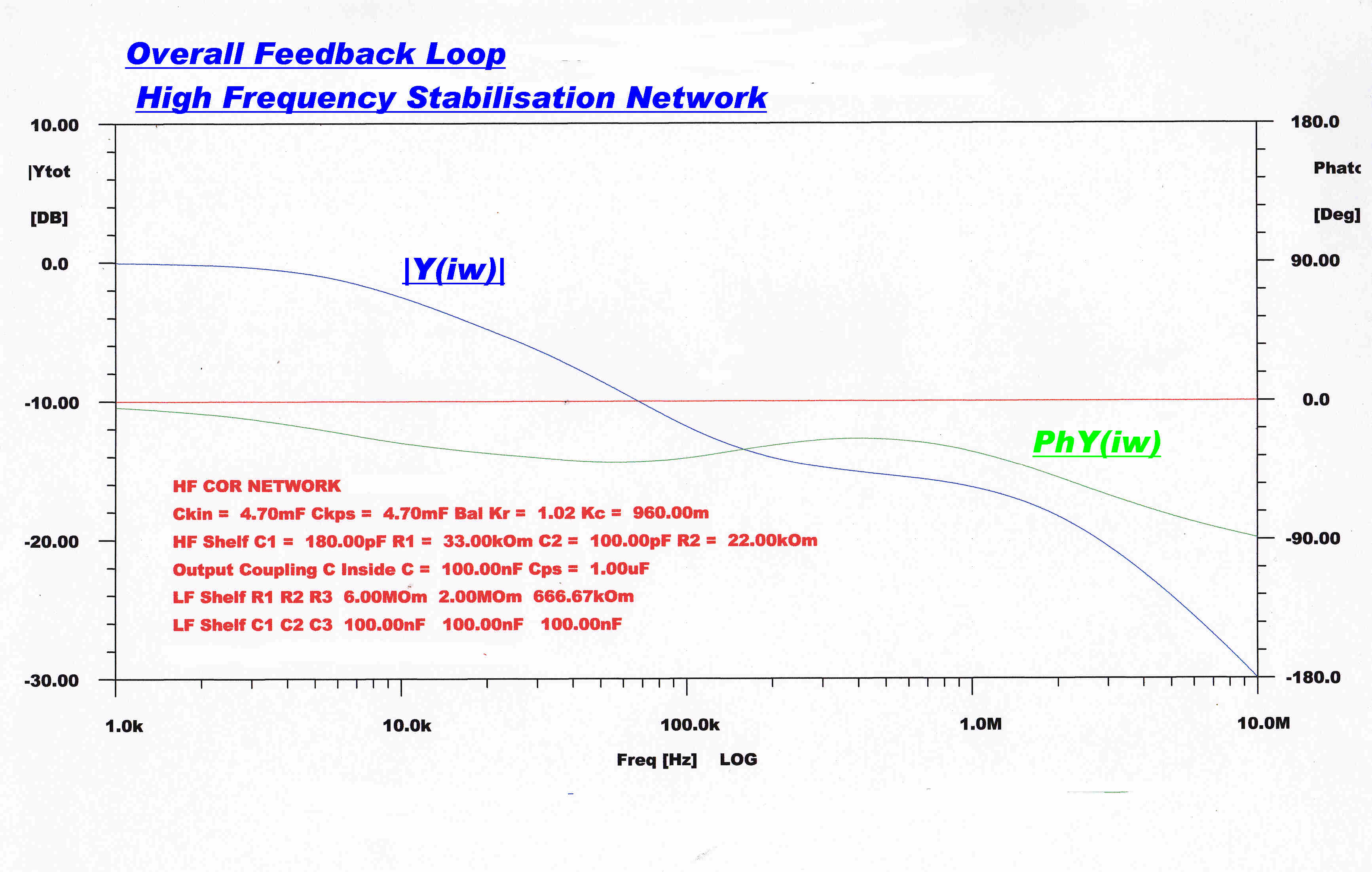 The response of the network is shown on the right
The network is made up of the 180pF,100pF,33K,22K R-C across
the 60K cascode load resistor.
At low frequencies the load on the cascode is 60K.
At high frequencies the load approaches 60k//33K//22K = 10.82K
The size of the shelf is then 60K/10.82K = 5.545 ( 14.88db)
Attenuation starts at about 10KHz and, because the slope is less
than 6db/octave, ends at about 150KHz.
The small decrease in overall feedback at 20KHz is considered of little
consequence because of the high degree of feedback.
The topology of the stabilising network shifts the high frequency
pole associated with the capacity in the cascode output.
If the output resistance of the cascode is high, the time constant for
the pole on the real axis is RC (60x103) C.
But the ultimate load is 10.82K, so the pole now has a time constant of
10.82x10³C - a much higher cutoff frequency - which removes it
beyond the active frequency range of the overall loop.
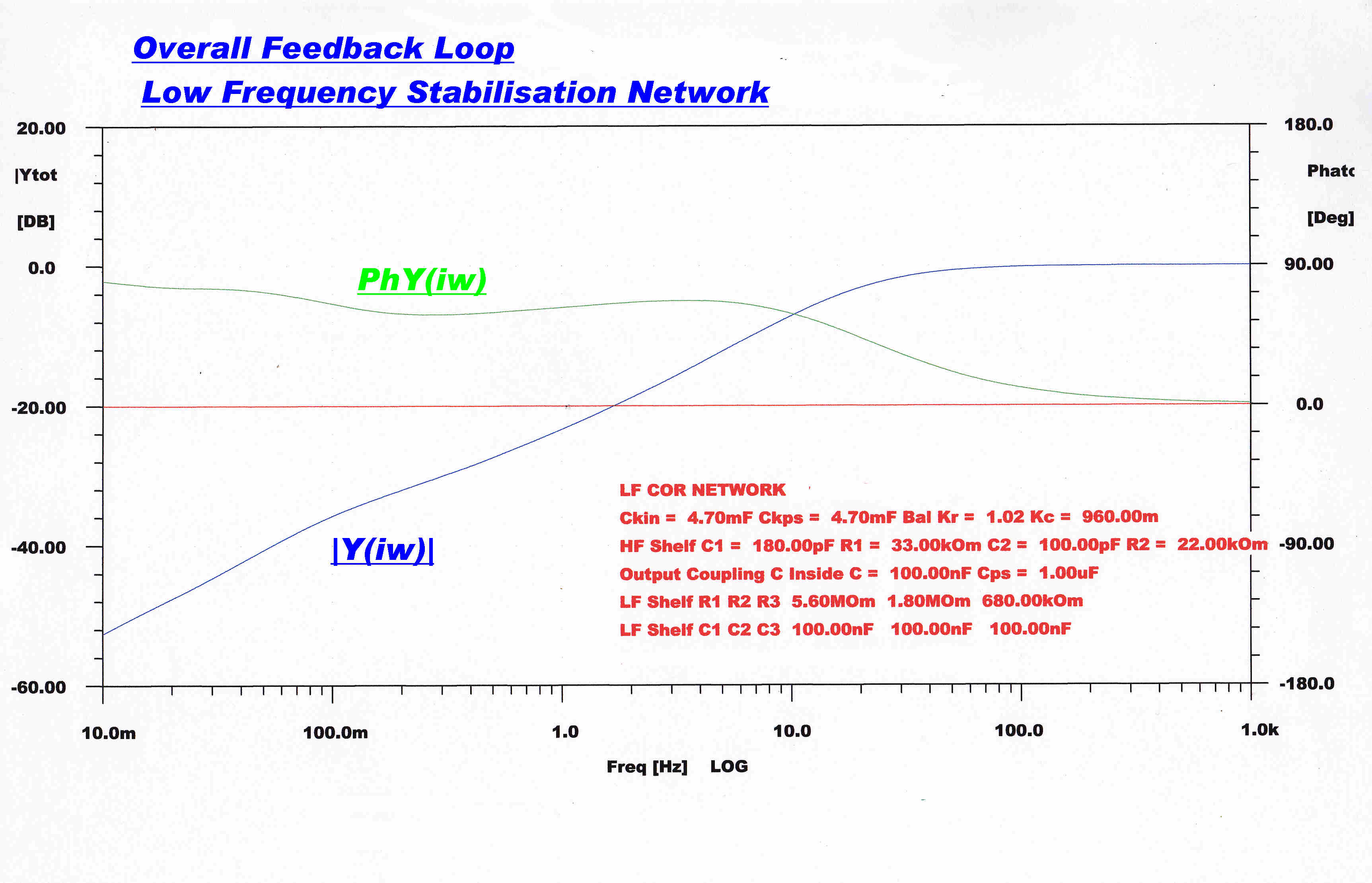 The response of the network is shown on the right.
It consists of the 6.6Meg, 1.8Meg, 680K, 470K resistors and the four
0.1uF capacitors. It also provides DC isolation between the
cathode follower, V3a, and the grid of V5a.
The corrective shelf starts at about 20Hz and continues down to about 1Hz.
with a phase change of about 70 degrees.
The phase splitter should have a flat and stable gain near unity and
a phase change very close to 180 degrees over the working frequency
range of the amplifier.
An operational amplifier with high gain fulfills both requirements.
For the ECC88s in the cascode:-
GM = 5Ma/V : μ = 33 : RP = 6.6K
Since the cathode is bypassed with a 4700uF capacitor RK = 0
From the equations above, we get the Norton equivalent for the cascode:-
GM = 4.854Ma/V : Rout = 231K : RL = 60K.
So voltage gain A = 231.
The cathode follower gain = 0.967 to give an overall gain of 223.7.
The feedback network has a gain of 0.5 to give a forward loop gain of 112.
Both the quiescent operating conditions and gain of the 6L6 output
tubes are under heavy feedback [ ≈ 31db or x35.5 ]
The balance of the push-pull output stage is then virtually independent of the
output tubes.
Only a small adjustment in the phase splitter gain is necessary for perfect
overall balance.
The total 6L6 output current is summed in a 1 ohm common resistor.
For perfect balance there is no signal across this resistor.
To balance the amplifier apply a 2KHz square wave to the input.
Adjustment of the 3/27pF capacitor brings the front to zero and
the 100K pot. brings the top of the wave to zero.
The adjustments do not interact and give easy convergence.

|

|
|
BALANCE ADJUSTMENT |
BALANCE ADJUSTMENT |

|

|
|
BALANCE ADJUSTMENT |
BALANCE ADJUSTMENT |
The output transformer uniquely determines the
response of the forward path.
A transformer driven from a high impedance has two dominant high
frequency poles - one formed by the self capacity of the primary winding
and the other by the primary-secondary leakage inductance.
The primary inductance and reflected load form a low frequency pole.
Due to the iron core, the primary inductance is highly non-linear.
This non-linearity manifests in two ways:-
(1) The inductance varies with signal level.
It is small for low levels - rises to a maximum
≈ 800H and then falls off as the core saturates.
The low level inductance is also a sensitive function of any
DC bias current due to unbalance in the push-pull output.
For high levels the magnetising current is far from sinusoidal
and the usual definition of inductance breaks down.
If the low frequency stability depends on transformer response,
it is possible to imagine an amplifier starting low frequency
oscillation at a low level and then the level stabilising as the
amplitude builds up.
(2) Driving the transforner primary from a zero impedance source will
still result in distortion.
The non-linear voltage drop across the primary resistance caused by
the non-linear magnetising current presents a distorted internal
drive voltage.
The overall feedback, then, must come from the secondary.
The output stage supplies both the load and magnetising current.
As the magnetising current increases, the maximum available load
current decreases, and so limits the power output from the
amplifier at low frequencies.
We can get a very rough estimate of the position of the two high
frequency poles asscociated with the output transformer:-
POLE 1 :- Formed by the primary winding capacity ≈ 500pF and
the reflected load 3500 ohms.
Τ = RC = 500x 10-12 x 3500 = 1.75x10⁻⁶ ::
fc = 1/( 2 Π Τ ) = 168KHz.
POLE 2 :- Formed by the primary seondary leakage inductance
≈ 10.76mH and the reflected load 3500 ohms.
Τ = L/R = 10.76 x0-3 / 3500 = 3.09x10⁻⁶ ::
fc = 1/( 2 Π Τ ) = 95.6KHz.
Analysis shows that a forward path with two poles this close will tolerate
little feedback before developing a peak in the steady state response and
severe ringing in the transient response.
Two stratigies are adopted to overcome the problem:-
[A] Up to about 40KHz, feedback is derived from the transformer secondary.
Beyond this frequency, feedback reverts to the primary, reducing
the transformer to a one pole system.
[B] A shelf is introduced into the forward path which starts to
introduce attenuation from about 10KHz
For normal operating levels, the transformer low frequency cutoff
is given by:-
Lpri ≈ 800H : RL = 3500 ohms :
Τ = Lpri / RL ≈ 0.229S :
fc = 1/( 2 Π Τ ) = 1.29Hz.
The lowest audio frequency applied to the amplifier is estimated as 20Hz,
so the low frequency shelf was designed to attenuate between 20 and 1 Hz.
This gives a large phase margin to accomdgate any decrease in inductance at low levels.
The cutoff frequencies of the plate current loop, the phase splitter, and the
cascode input are below 1Hz , so do not affect stability.
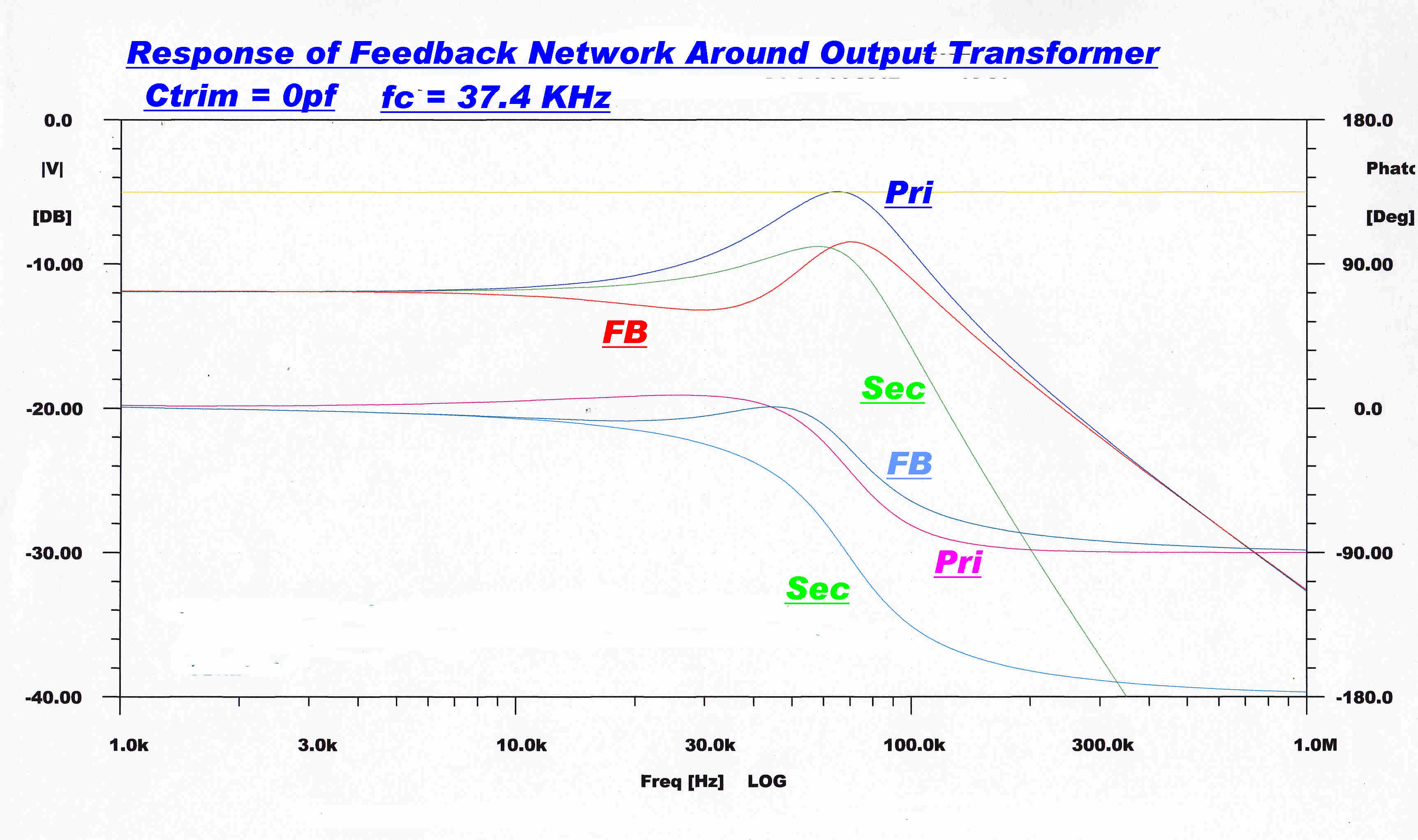 Suppose we connect a capacitive voltage divider to the primary of
the transformer and a resistive voltage divider to the secondary.
Make the division ratio of the capacitive divider equal to the
transformer division ratio by the resistive divider ratio.
If the transformer is ideal, the voltage output from both dividers
is identical - so their outputs can be joined.
At high frequencies the impedance of the capacitive divider
falls below that of the resistive divider, so it wll predominate.
The primary voltage determines the output from the network at high
frequencies, and so the extra pole associated with the primary
- secondary leakage inductance is eliminated from the forward path.
The turnover frequency is easily calculated using Thevenin.
The output capacity of the divider is the sum of the two capacities:
the output resistance of the secondary divider is given by the two resistors
in parallel : the time constant is the product of the two.
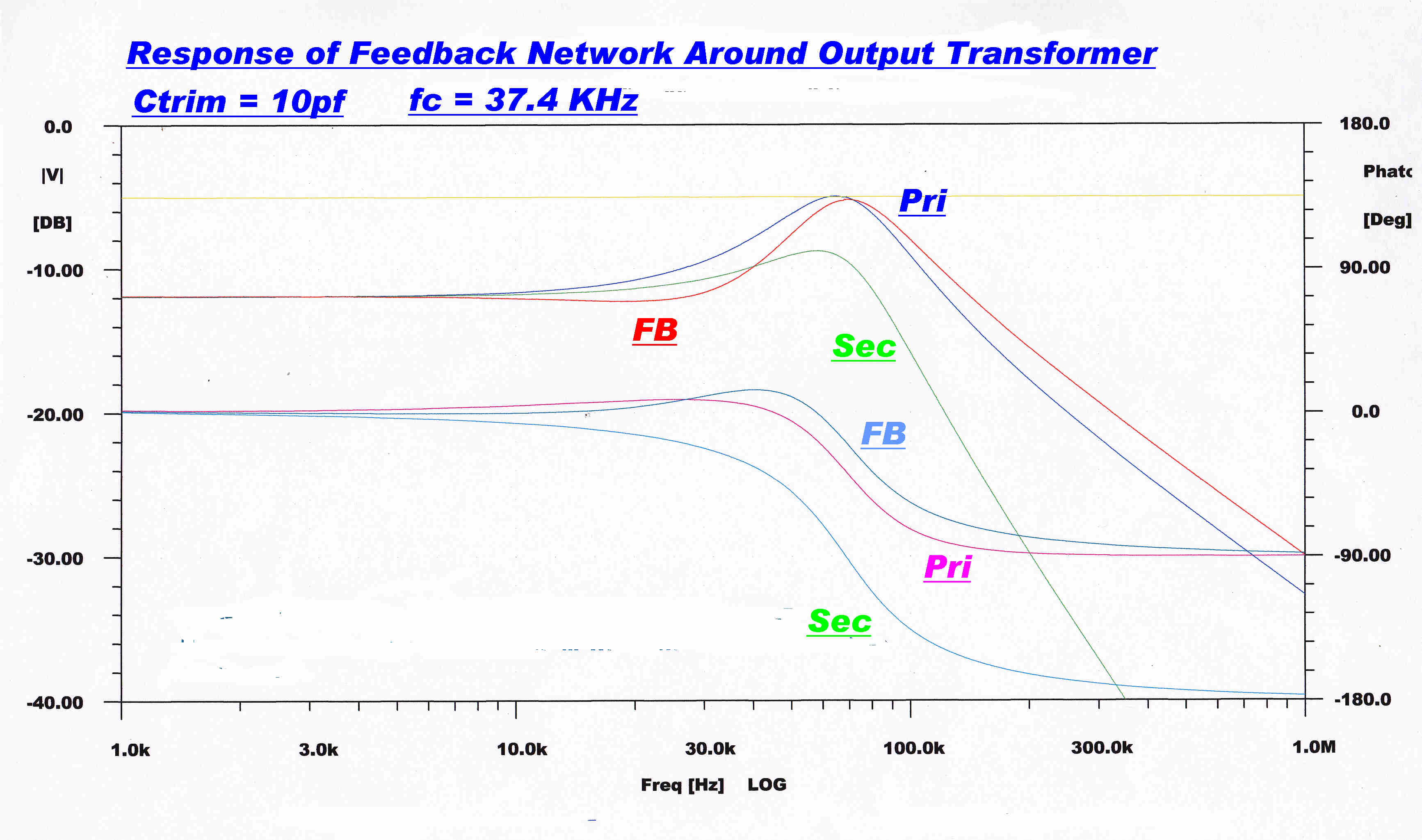
The above plot shows the steady state response of a current driven
transformer surrounded by a network with a cutoff frequency of 37.4KHz
Note: The ultimate slope of the primary and network voltage is 6db/octave
and the secondary 12 db/octave because of the extra pole.
The ultimate phase change of the primary and the network is 90 degrees,
while the secondary goes to 180 degreees.
The transfer function of the transformer is not a constant as assumed,
but is modified by the leakage inductance.
This causes a dip in the response of the network at about 30 KHz.
This network is in the feedback path - not the forward path.
This results in a corresponding peak in the overall response.
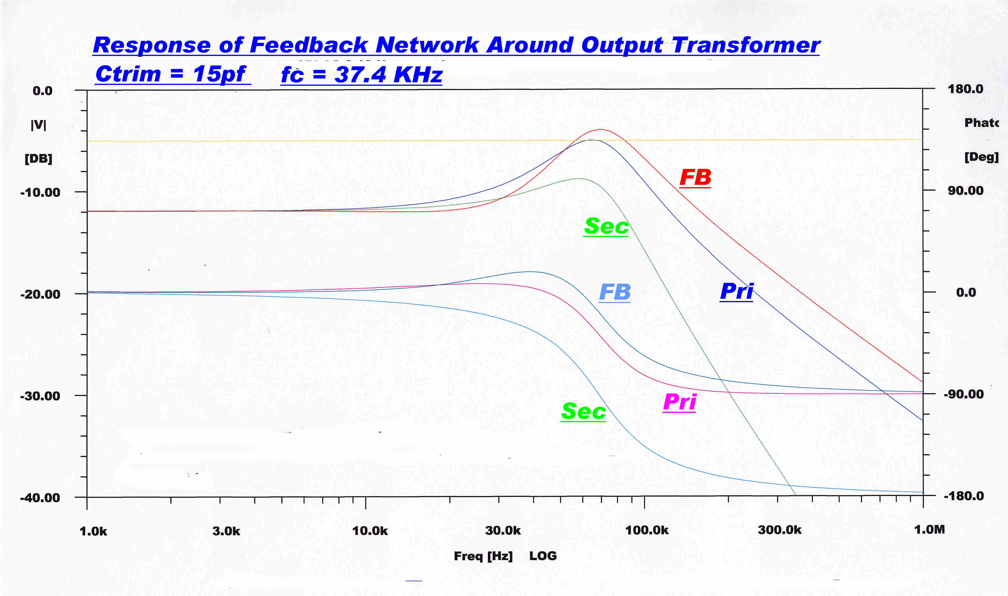
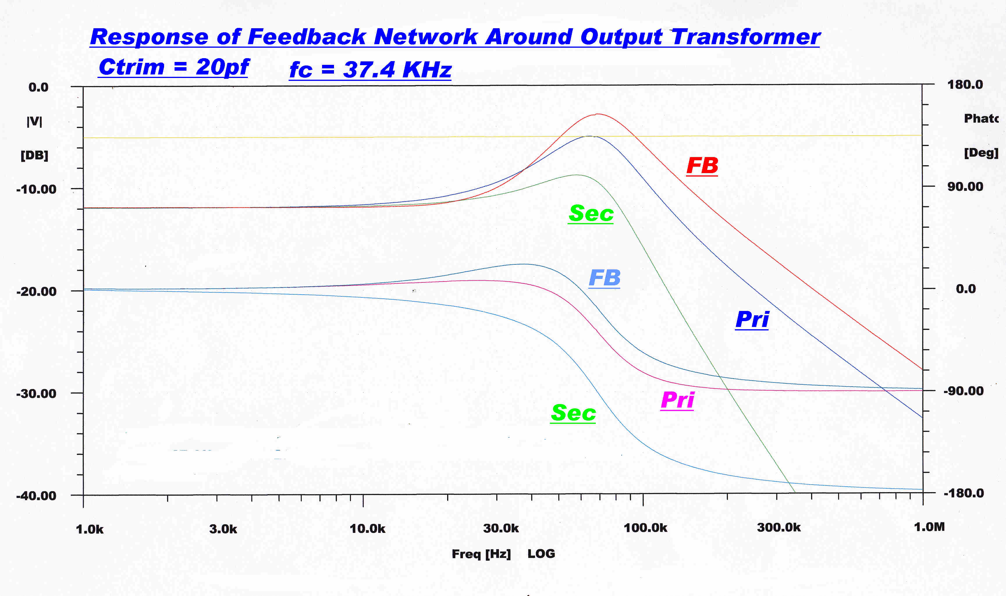
Computer runs show that an increase in the "top" capacity will
very nearly eliminate the dip, so the capacitor is made adjustable.
Setup is simple:- The front of the square wave output is adjusted
for best response.
The bottom resistor of 665 ohms is replaced by a 1.8K, 180 ohm and
1K adjustable potentiometer. This allows the convenient removal
of the overall feedback for test and fault finding.
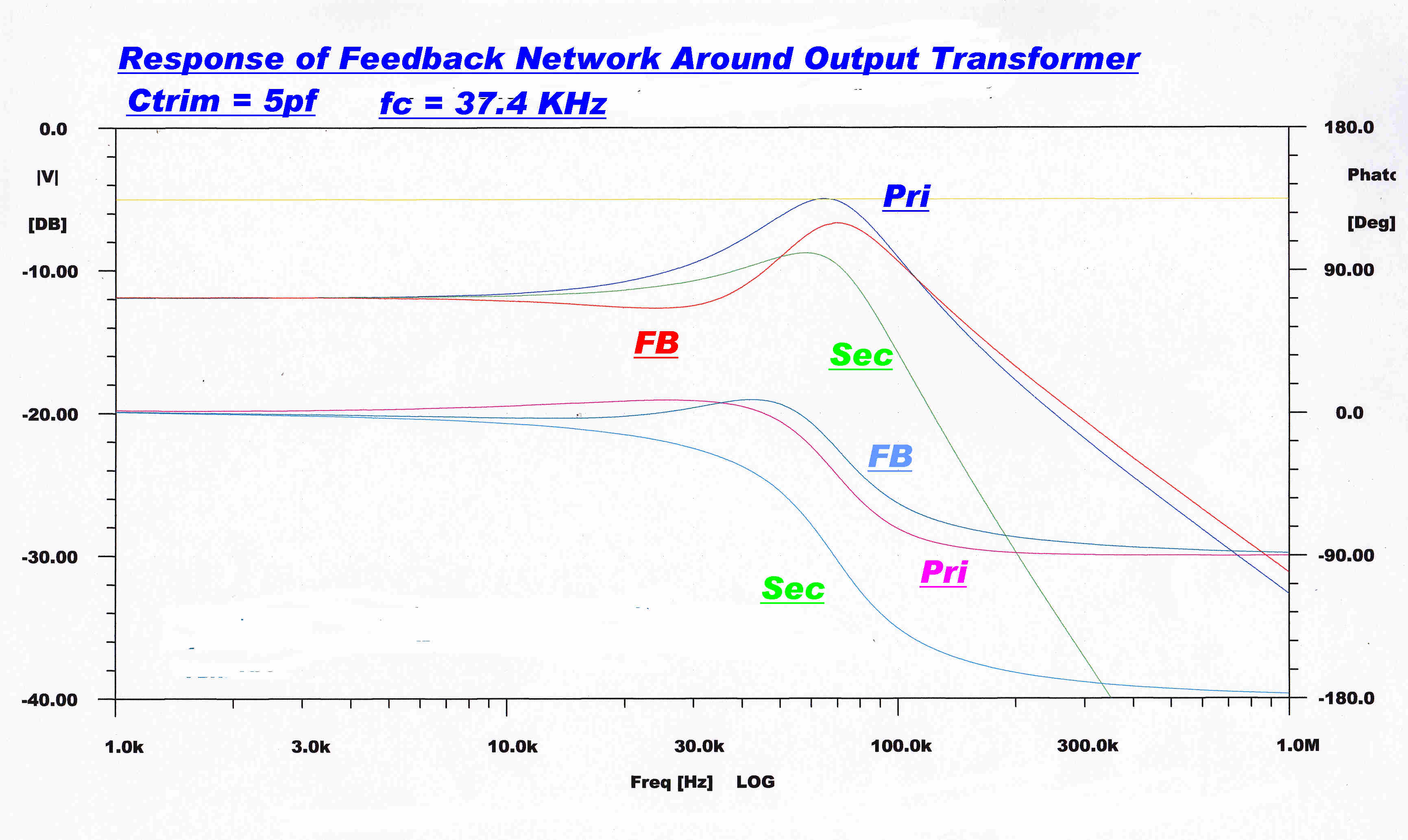
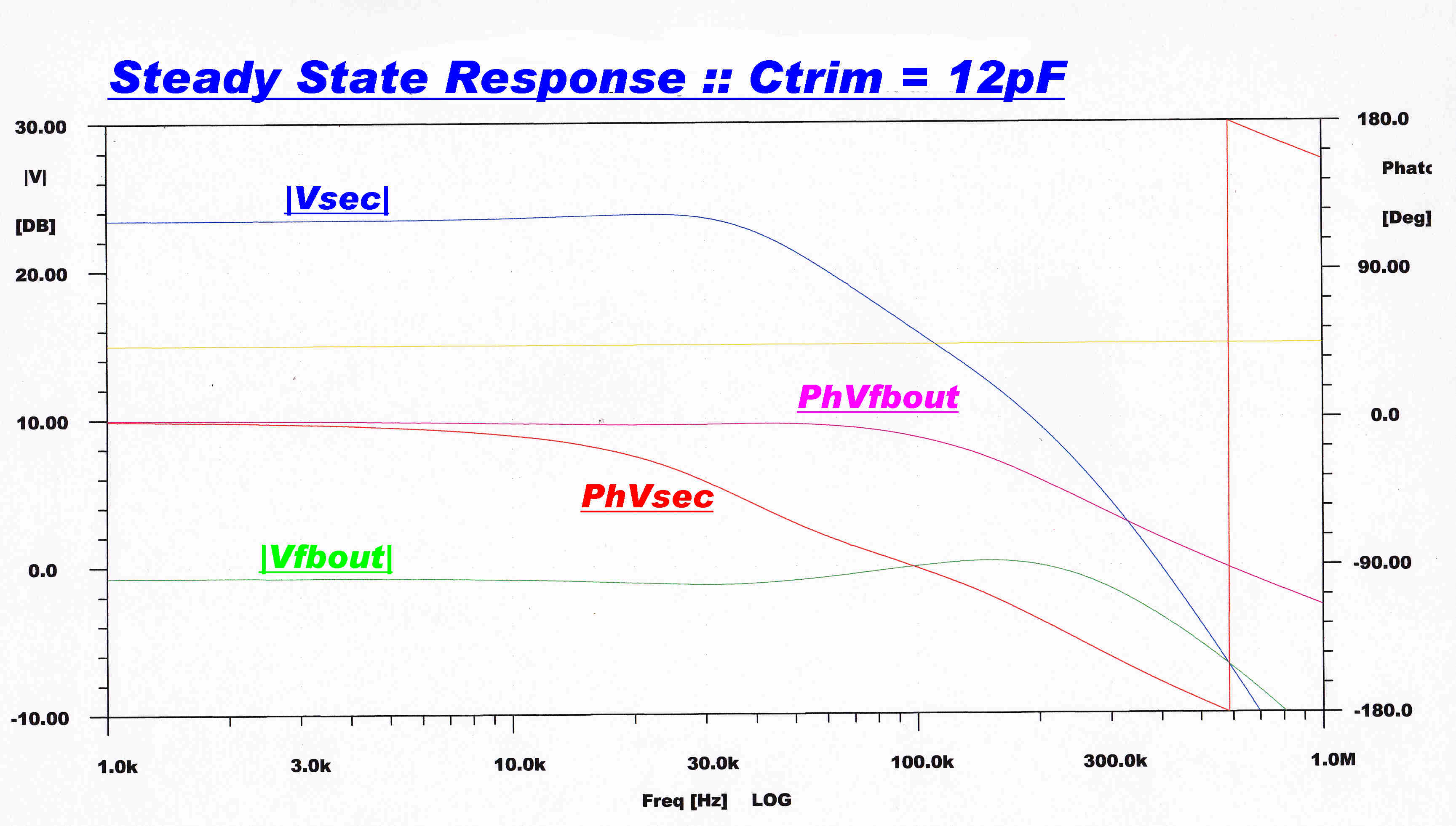
The change in the network response as capacity is added to
the "top" capacitor is shown in the following computer runs.

|
|
|
|
|
Note that for trim Cs from about 10pF to 15pF the primary response and the network response are very close. |
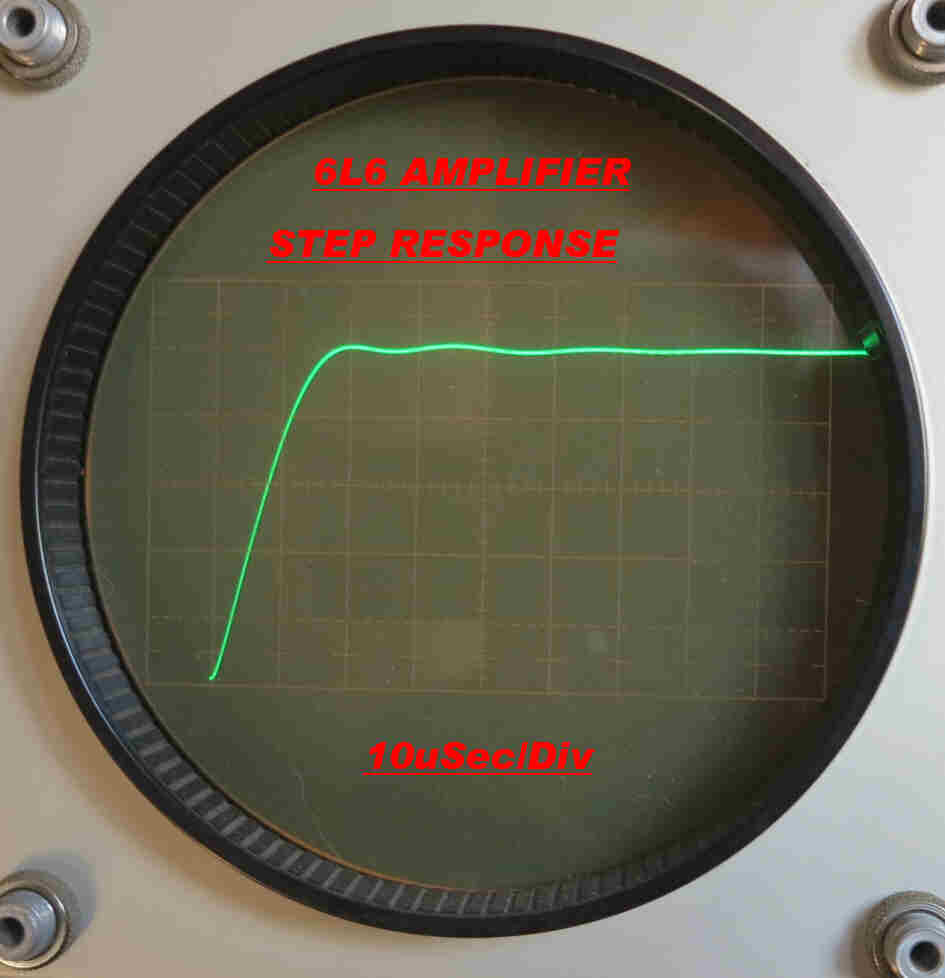 When the added trim C is correctly adjusted the front of
the step response looks like this.
Note:-Low level ringing at about 67KHz sometimes turns up in the test
results, but not in the computed waveforms.
Approximations in the computer model for the output transformer cause this.
Some of the approximations are:-
(a) The winding capacity is distributed, not lumped.
(b) The resistance of the windings is not constant, but increases with
frequency due to skin and proximity effect.
(c) The resonant frequency of each half of the primary winding is different.
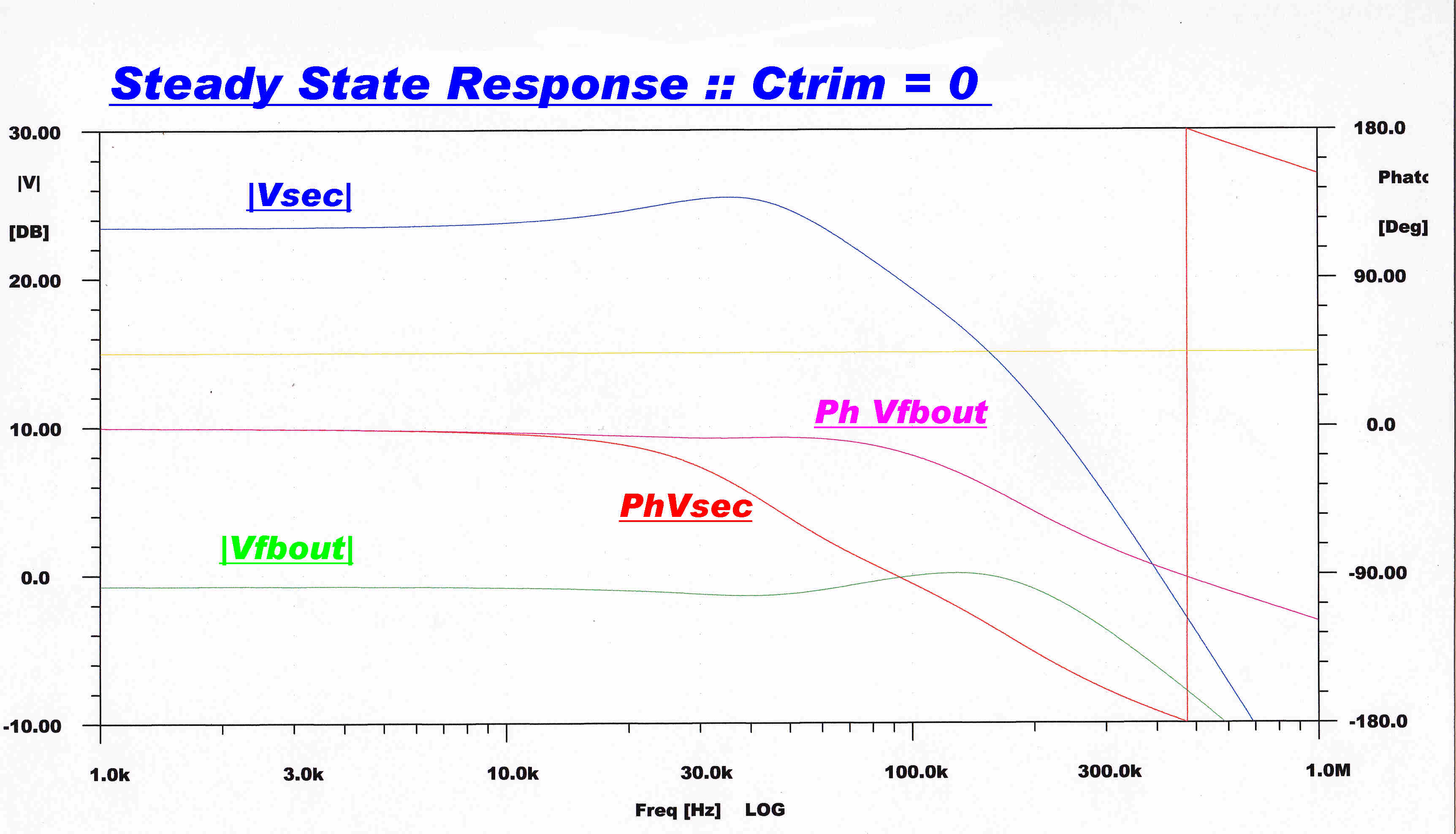
|
|
|
Overall ( Closed Loop ) Steady State Response |
Overall ( Closed Loop ) Steady State Response |
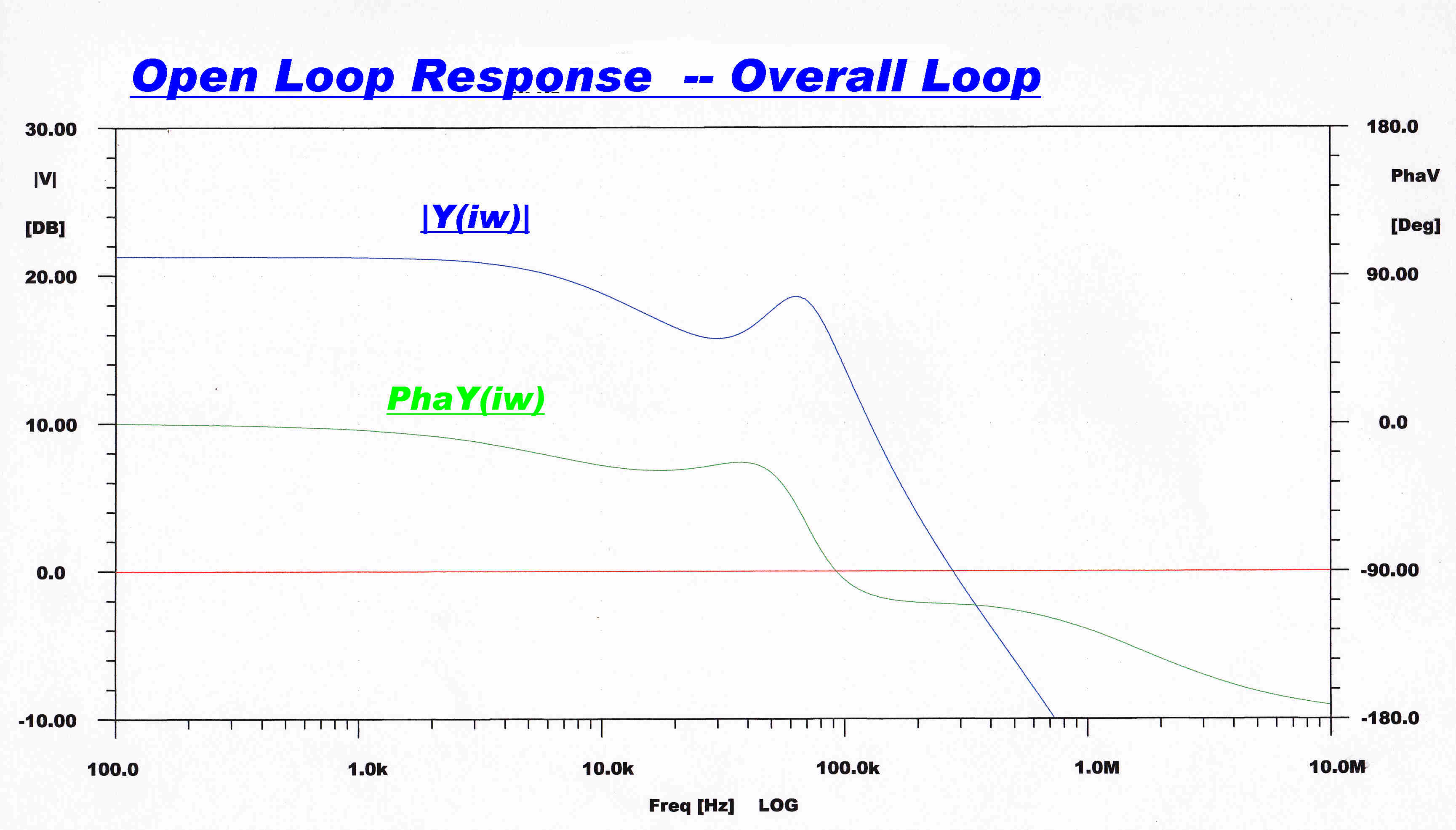
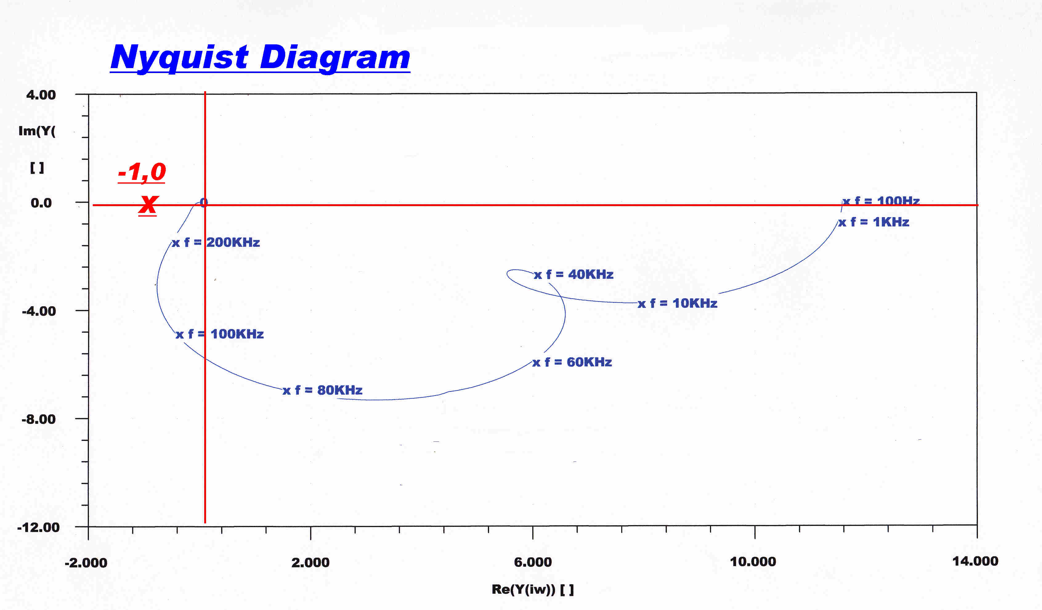
The open loop transfer function is shown below in Cartesian (Bode) and polar ( Nyquist ) form.
|
|
|
The open loop response reaches unity gain at a frequency of about 280 KHz. and a phase change of 110 degrees. This indicates a phase margin of 70 degrees - a stable amplifier with little ringing in the transient response. |
The same information but in polar form. |
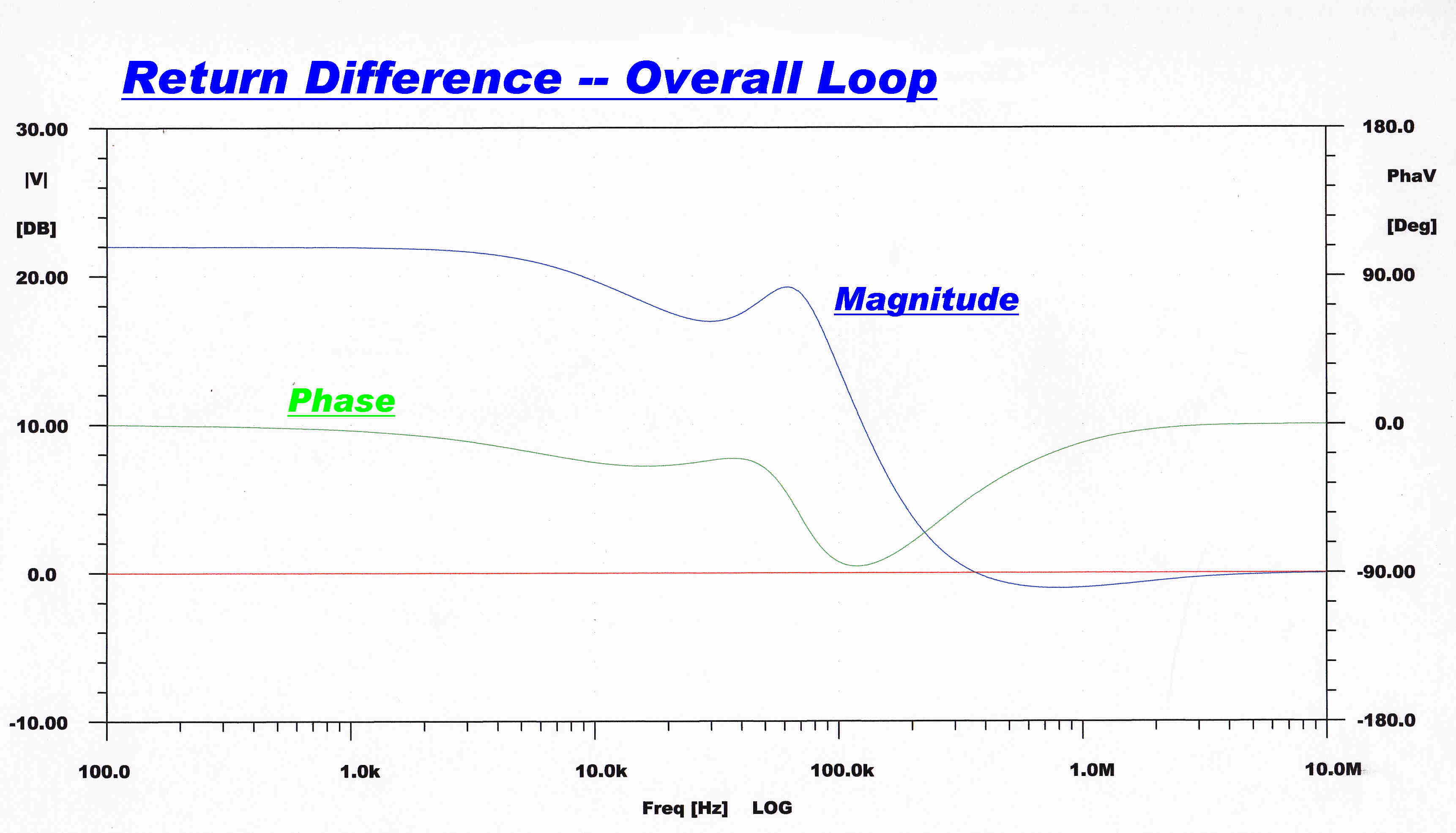 A plot of the return difference in the overall loop
is shown opposite.
The magnitude of the return difference gives a measure
of the reduction in distortion.
The return difference is 22db ( x12.6) up to about 5KHz
falling off to 18db (x7.9) at 20KHz.
This reduction is considered of little consequence, since
the total return difference on the 6L6 output stage from
current feedback is 31.2db (x36.5).
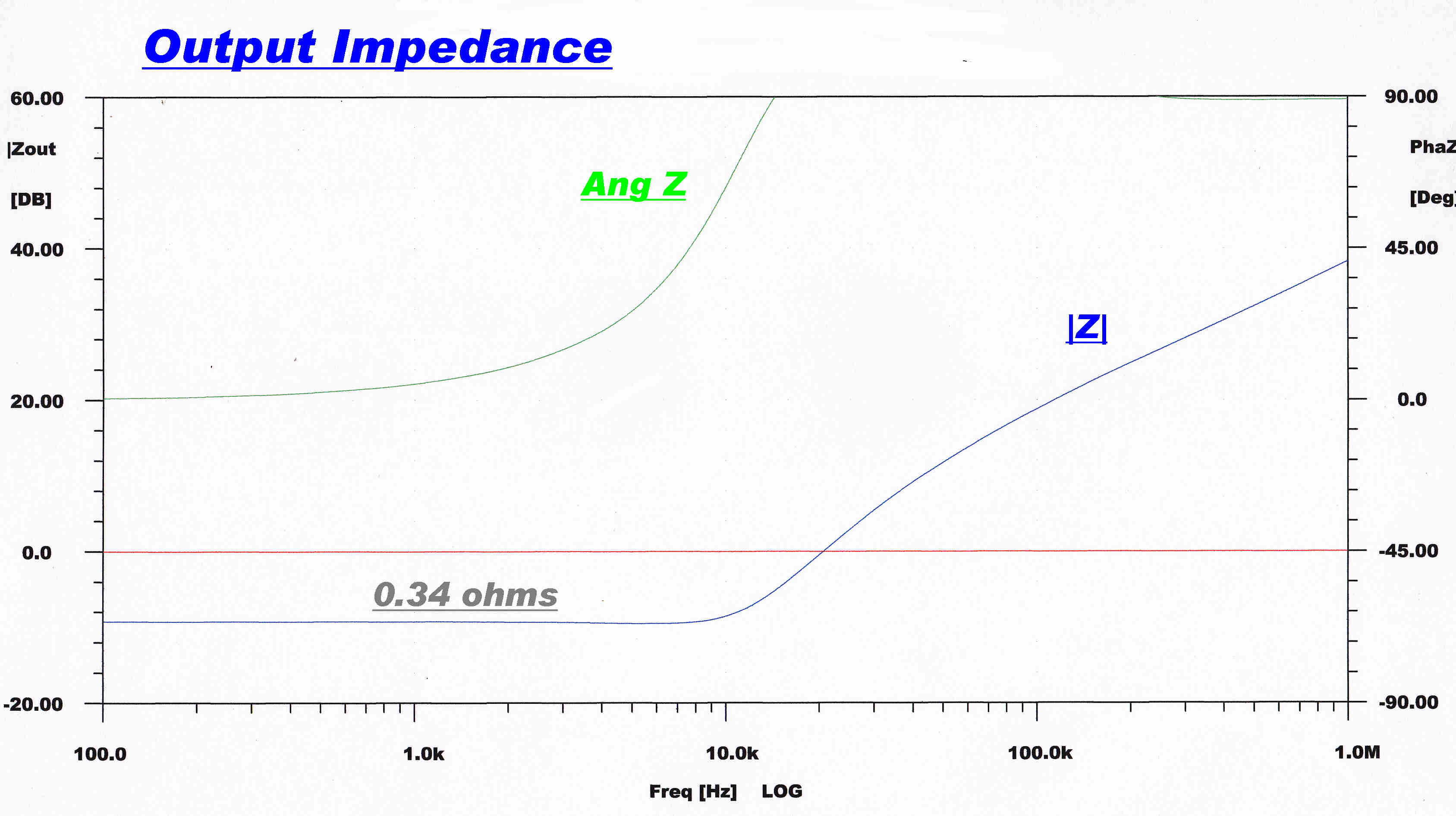
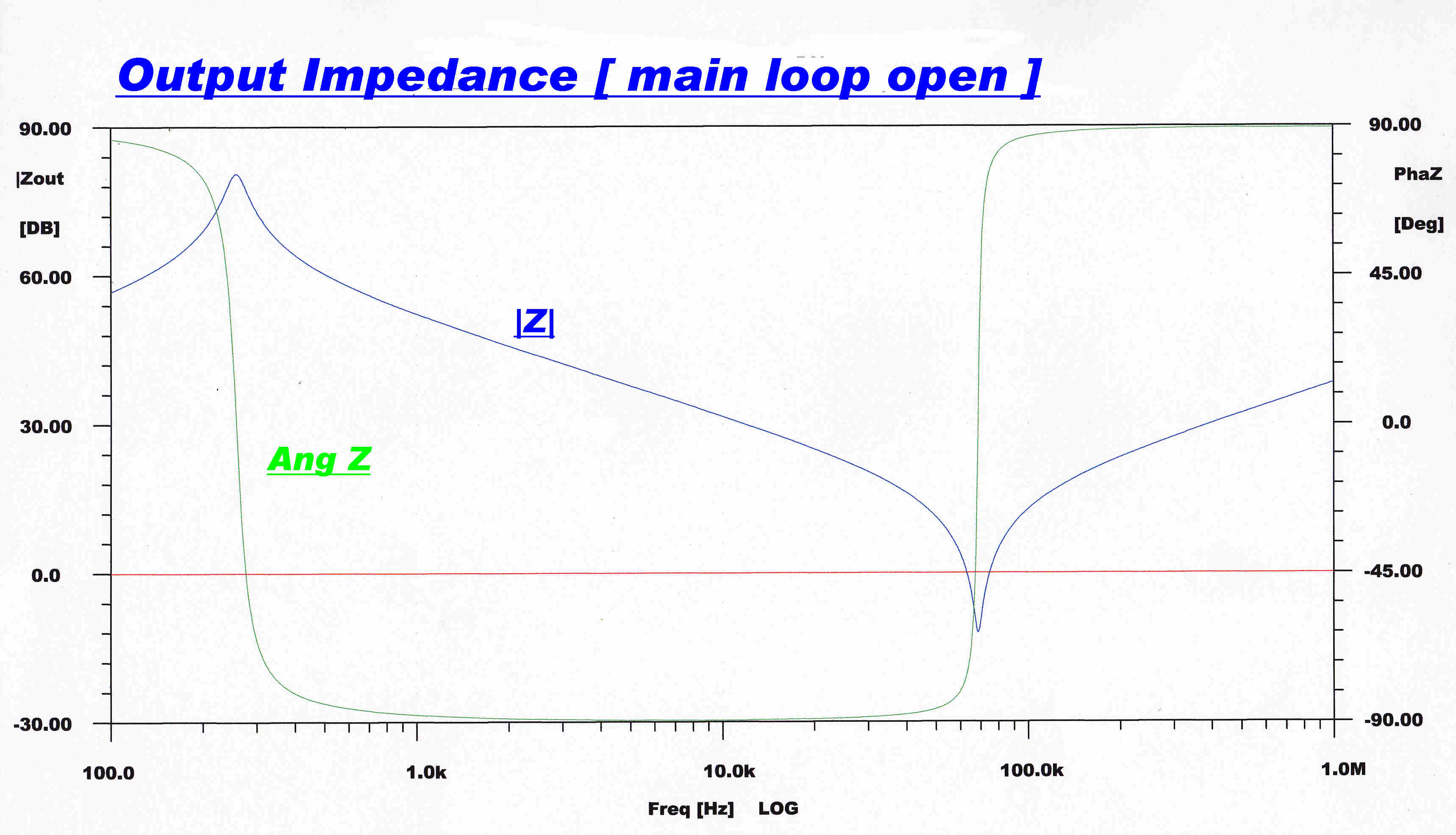
The amplifier output impedance with the overall loop closed (LHS) amd open (RHS).
|
|
|
The output impedance is measured looking into
the amplifier terminals setup to drive a 4 ohm load. |
Since the primary of the output transformer is driven by
a current generator, the low output impedance depends entirely on the
overall feedback loop. |
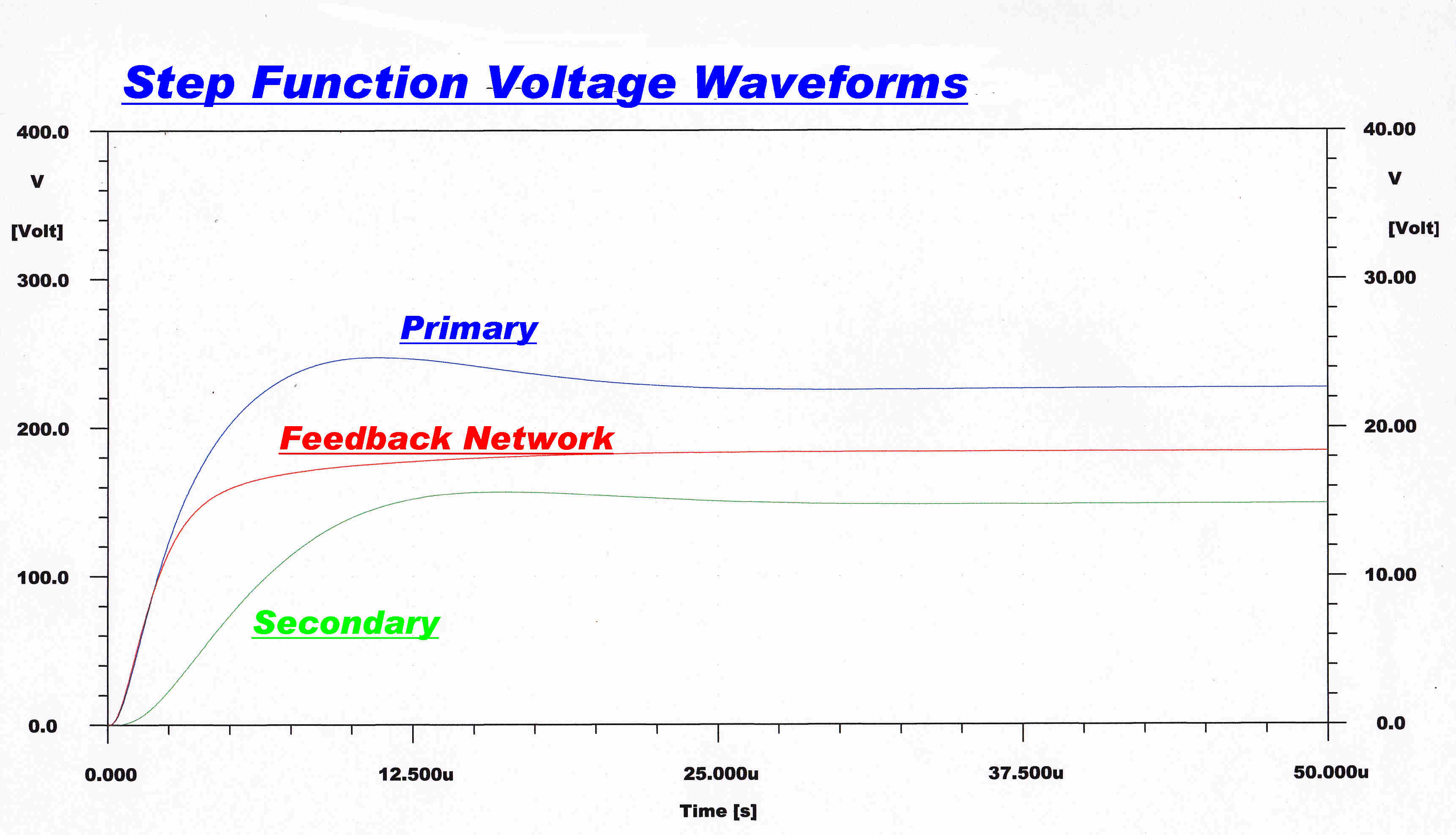
It is interesting to study the waveforms through out the
amplifier for a step function input.
A step with a very fast front will overload the input stages of a
feedback amplifier.
The low pass R-C filter at the input to the amplifier will slow the
front down and prevent this.
The response of this filter is given by:-
Vo(t) = 1 - e-t/τ where τ = 2.21μS
This was used as the input waveform in the computer program
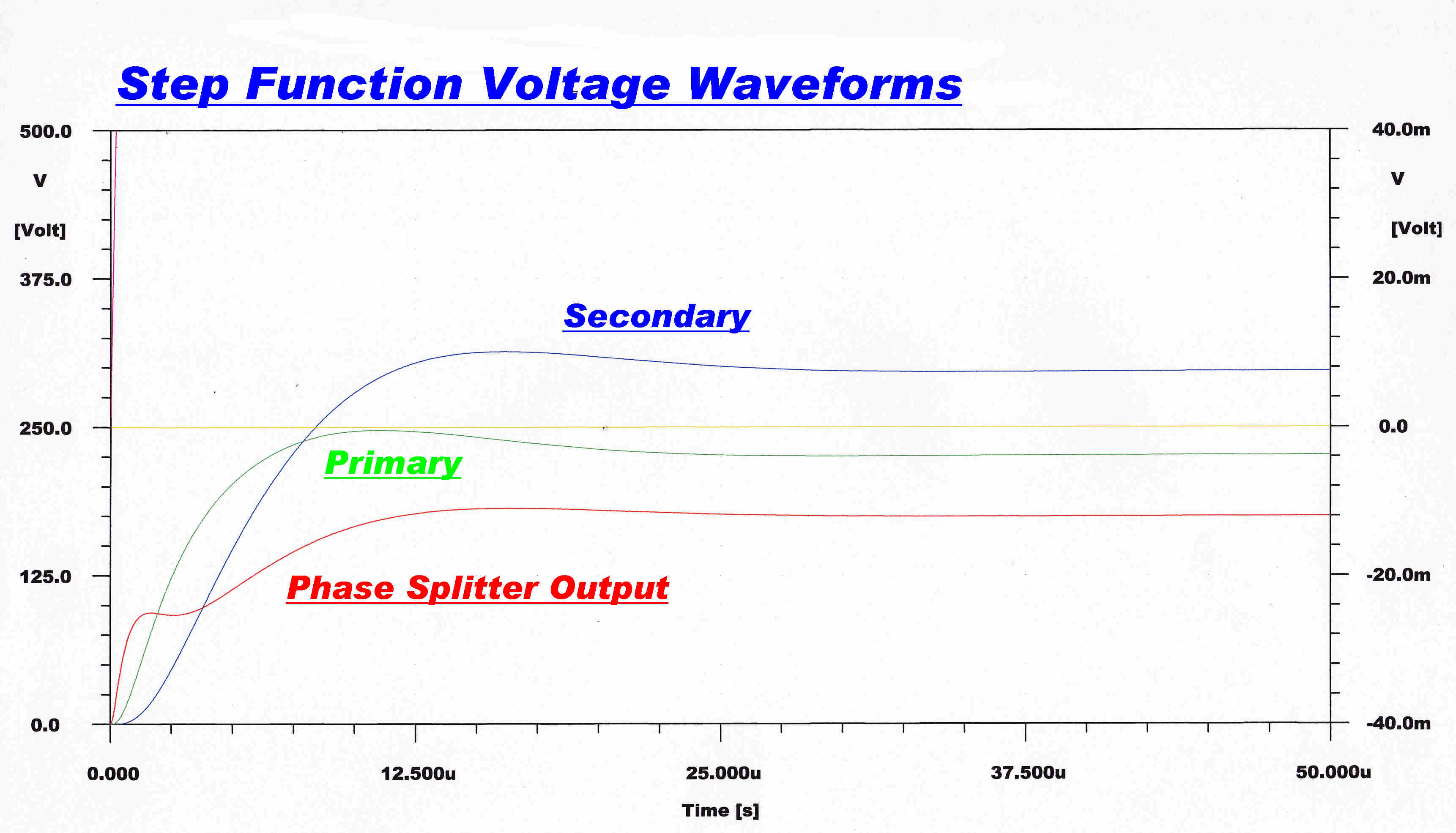
|
|
|
Computed Result |
Test Result |
|
|
|
Computed Result |
Test Result |
It is interesting to evaluate some of the pressures in
a sound wave:-
At standard temperature, atmospheric pressure
p = 105 N/M2
Density ρ = 1.18 Kg/M3
Velocity c = 344.8 M/S
Characteristic impedance Zo = ρ c = 406.86 ohms
Intensity I = p2/Zo = p2/(ρ c )
W/M2 ----(1)
The intensity for 0db reference level ( threshold of hearing ) is
defined as: I = 10-12 W/M2
Substituting in (1) above we have pref = 2x10⁻⁵
N/M2
If the level rises to 100db, the sound pressure is still only
2 N/M2 on top of 105 N/M2
- still a very small perturbation of atmospheric pressure.
It is important to retain the light level in a scene, so video channels are inherently DC coupled
Rise-time, overshoot and ringing associated with the
high frequency response are well known - sag and droop, the low frequency
transient parameters, less so.
A few of the salient features of low frequency transient response
theory are now outlined.
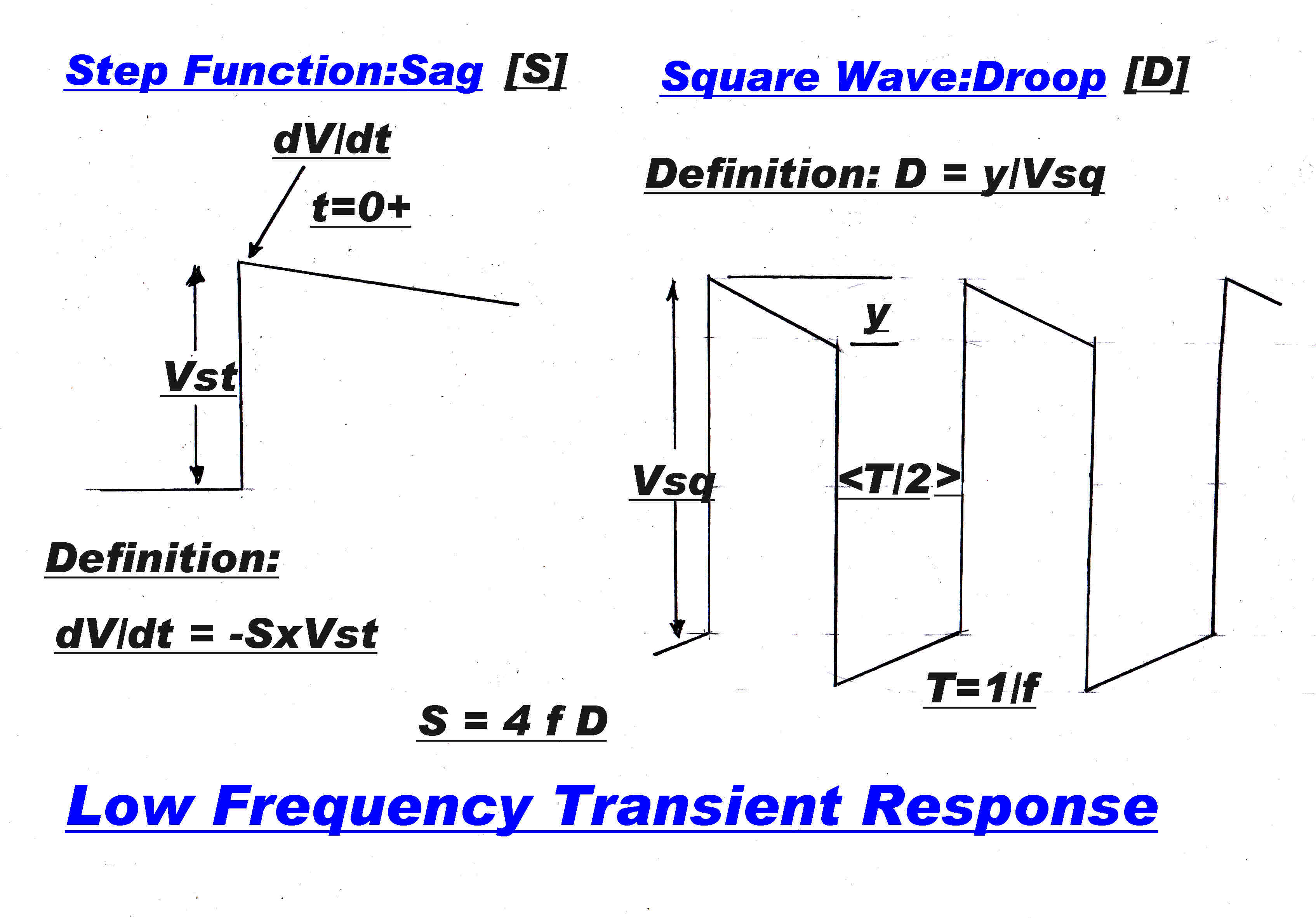 If the step response of an AC coupled system is normalised to
1, then the negative of the slope immediately after the step is called the "SAG" S.
The time just after the step is designated as t = 0+
The definition of "DROOP", D, for a square wave is given opposite.
The relationship between the two is given by:-
S = 4 f D
where f is the frequency of the square wave.
The sag S can be extracted from the low frequency
transfer function.
It can be shown that:-
S = Lt [ p( YN(p) - 1 ) ] as p--> ∞
where YN(p) is normalised to give unit step output.
The normalised transfer function of an R-C coupling network used in the
amplifier is given by:-
YN(p) = τp/( 1 + τp )
so for this network the sag is given by:-
S = Lt p[ τp/( 1 + τp ) - 1 ] as p --> ∞
ie S = 1/τ
If we expand the normalised transfer function into a series we have:-
YN(p) = 1 + a1/p + a2/p2
+ a3/p3 . . . . . . .
where the first term is 1 because the transfer function is normalised.
If we evaluate sag we have :-
S = Lt p[ 1 + a1/p + a2/p2
+ a3/p3 . . . . - 1 ] as p ---> ∞
ie S = a1
If we put a number of systems in cascade then the we multiply the
series representing each transfer function and the first term coefficients
add.
We then have the useful result:-
Since we can design networks with sags of opposite sign, equalisation of the slow speed transient response is easily accomplished.
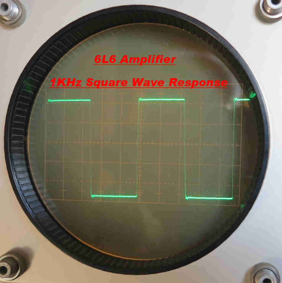
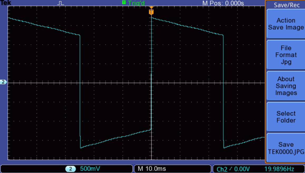 The small signal square wave response at 20Hz
is shown opposite.
This indicates an excellent response with a droop of about 0.17.
It is the response predicted by the linear theory used to design
the amplifier, and also the response given by the small signal
computer program.
The peak flux densities in the iron of the transformer core increase
inversely with frequency and eventually enter a highly non-linear
region at some low frequency.
This results in a change of wave shape and the distortion
illustratred below.
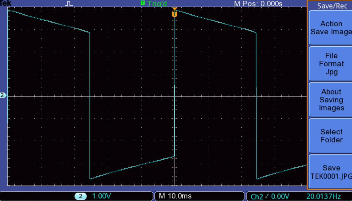
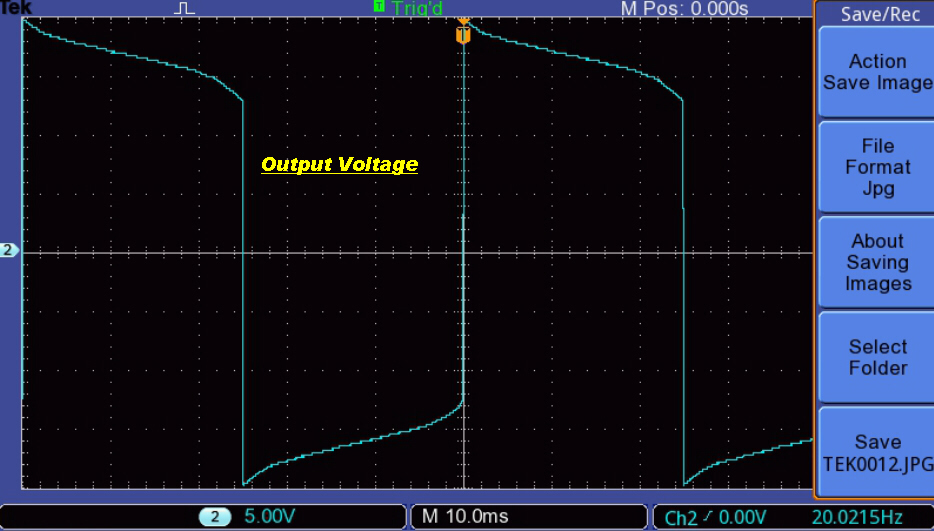
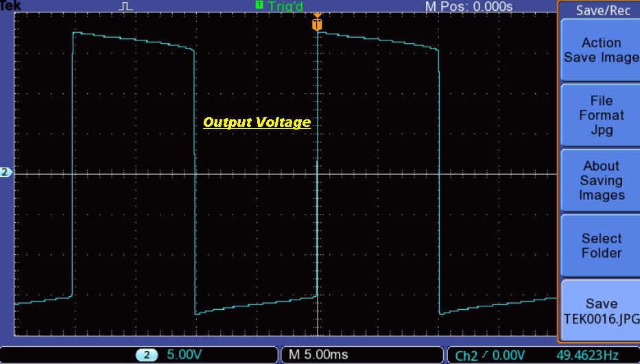
The effect of non-linear magnetising current is shown below:-
|
|
|
|
Low Level Output at 20 Hz. |
Near full output at 20Hz. |
Near full output at 50Hz. |
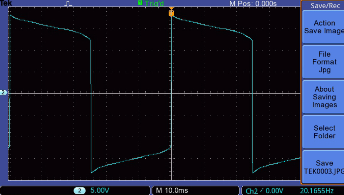
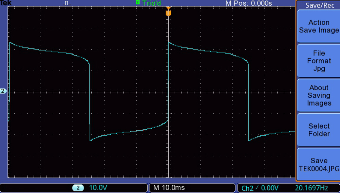
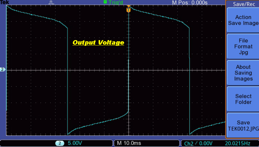
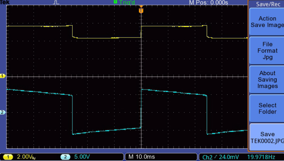
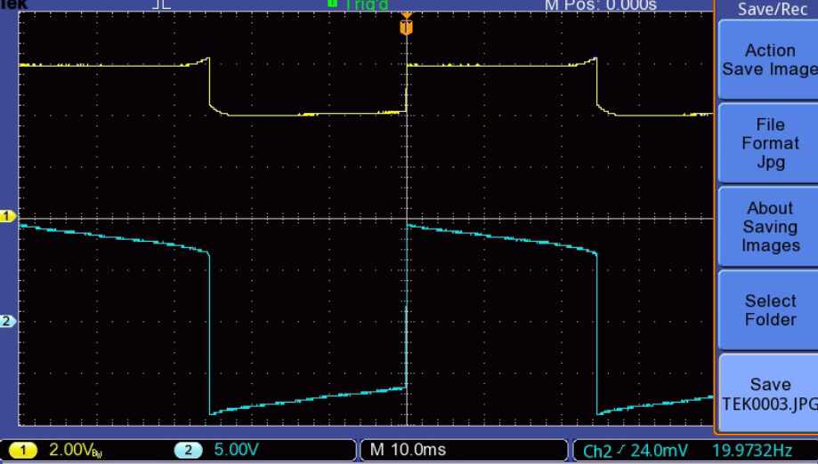
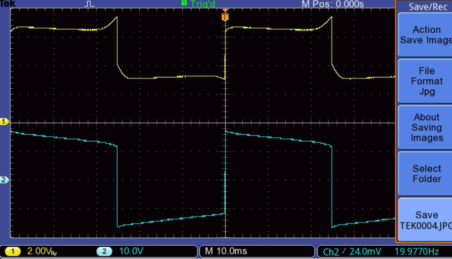
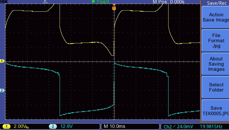
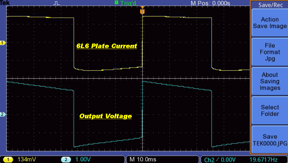
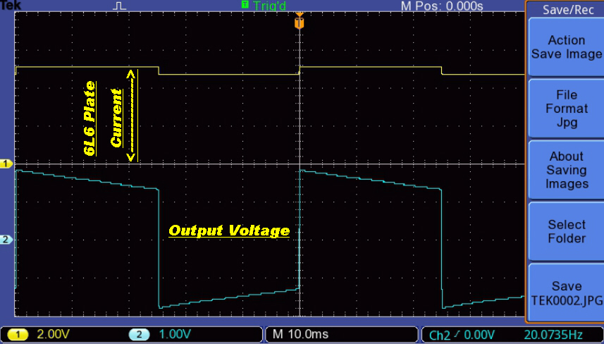
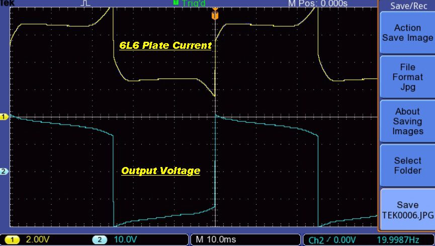
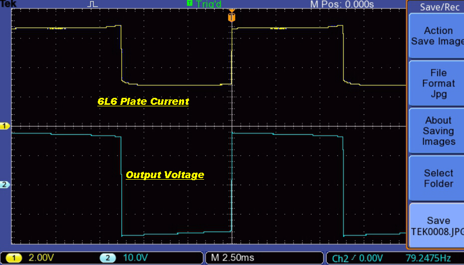
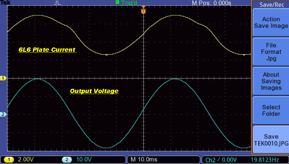
The change in waveshape with output level at 20 Hz is illustrated
below:-
The Y (voltage) scale is as follows:-
[1] 500mV/div
[2] 1Vdiv
[3] 2V/div
[4] 5V/div
[5] 10V/div
[6] 5V/div

|

|

|
|
|
|
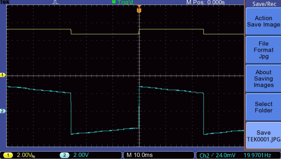
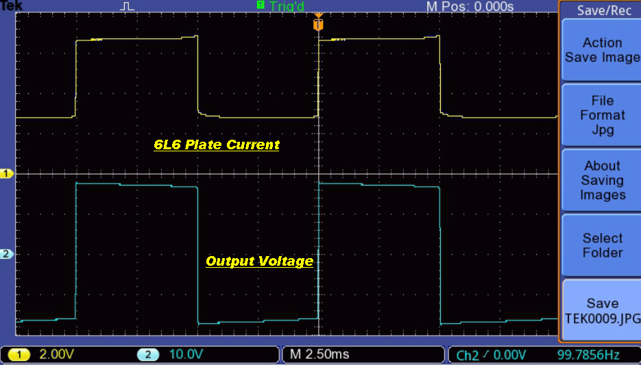
The increase in peak magnetising current with increase in output at 20Hz. is illustrated below:-
|
|
|
|
|
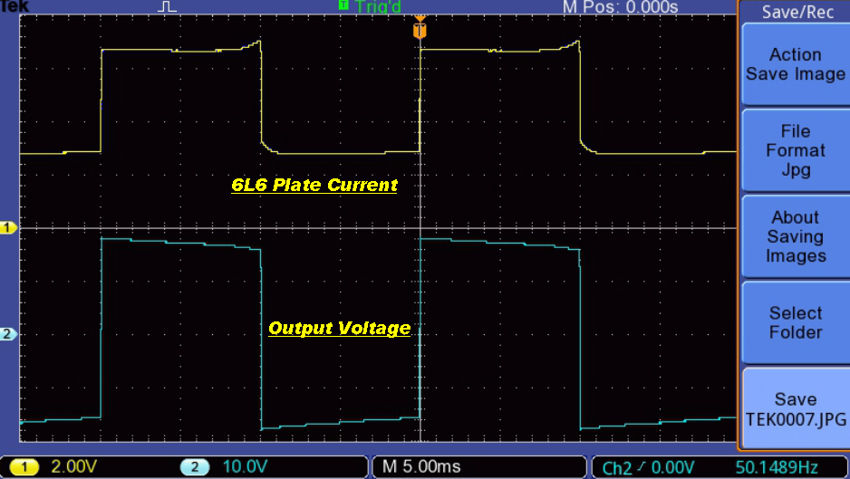
The upper trace (yellow) is the plate current drive with zero DC
on the x axis. |
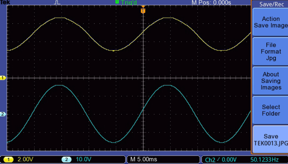
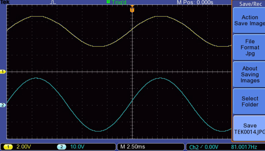
The decrease in peak magnetising current with increase in frequency
is illustrated below:-
The frequencies are:-
[1] [2] [3] 20Hz
[4] 50Hz.
[5] 80Hz.
[6] 100Hz.
|
|
|
|
|
|
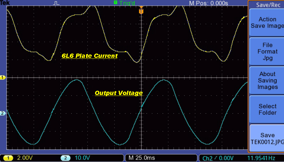
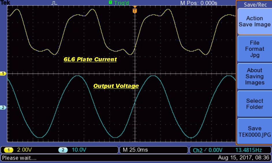
The magntising current for sinusoidal outputs is shown below:-
Frequency:-
[1] 12Hz.
[2] 13.5Hz.
[3] 20Hz.
[4] 50Hz.
[5] 80Hz.
[6] 100Hz.
Note that the output waveform at 20 Hz. looks clean although the transformer
prinary current has a kink.
|
|
|
|
|

|
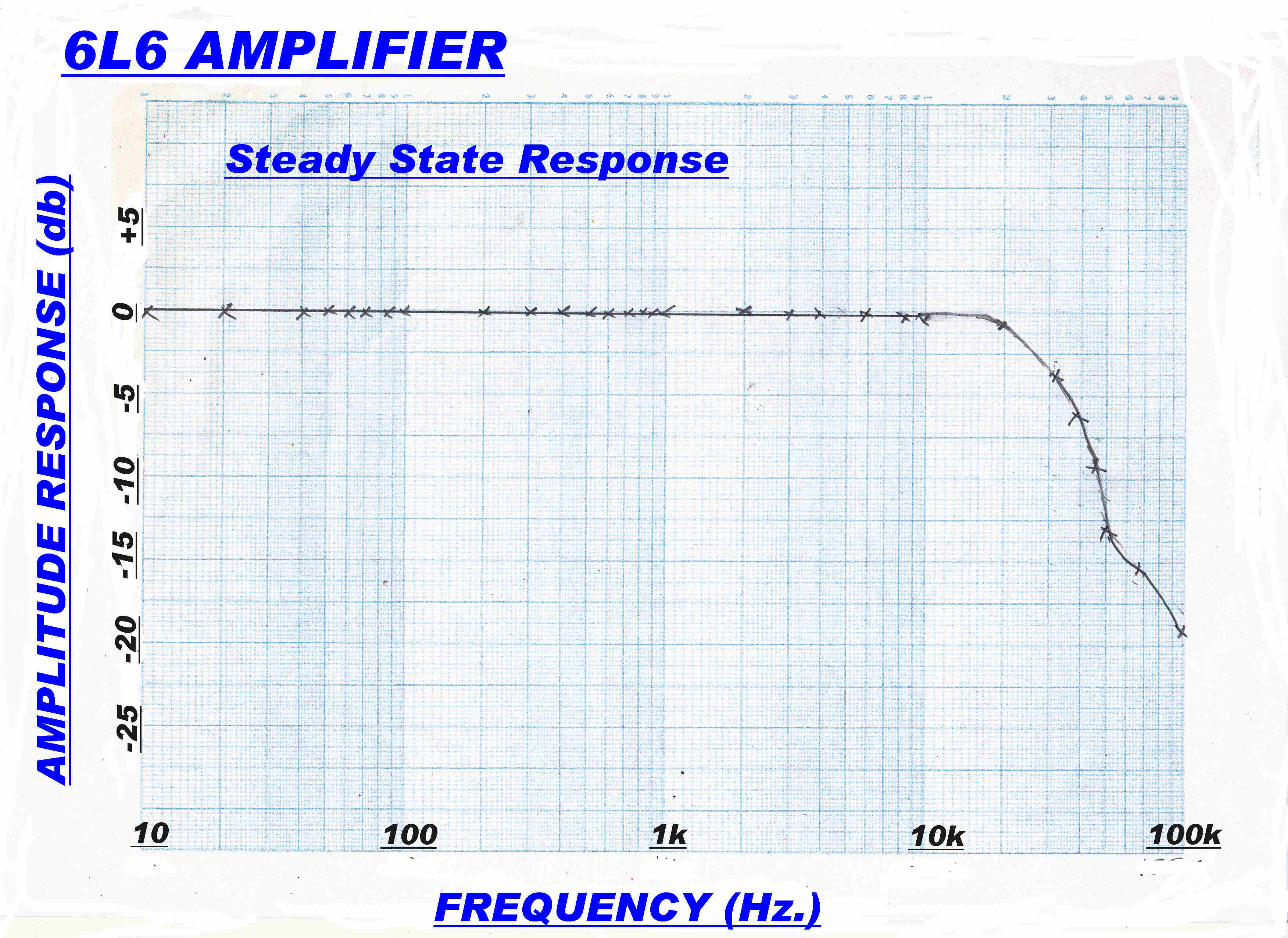
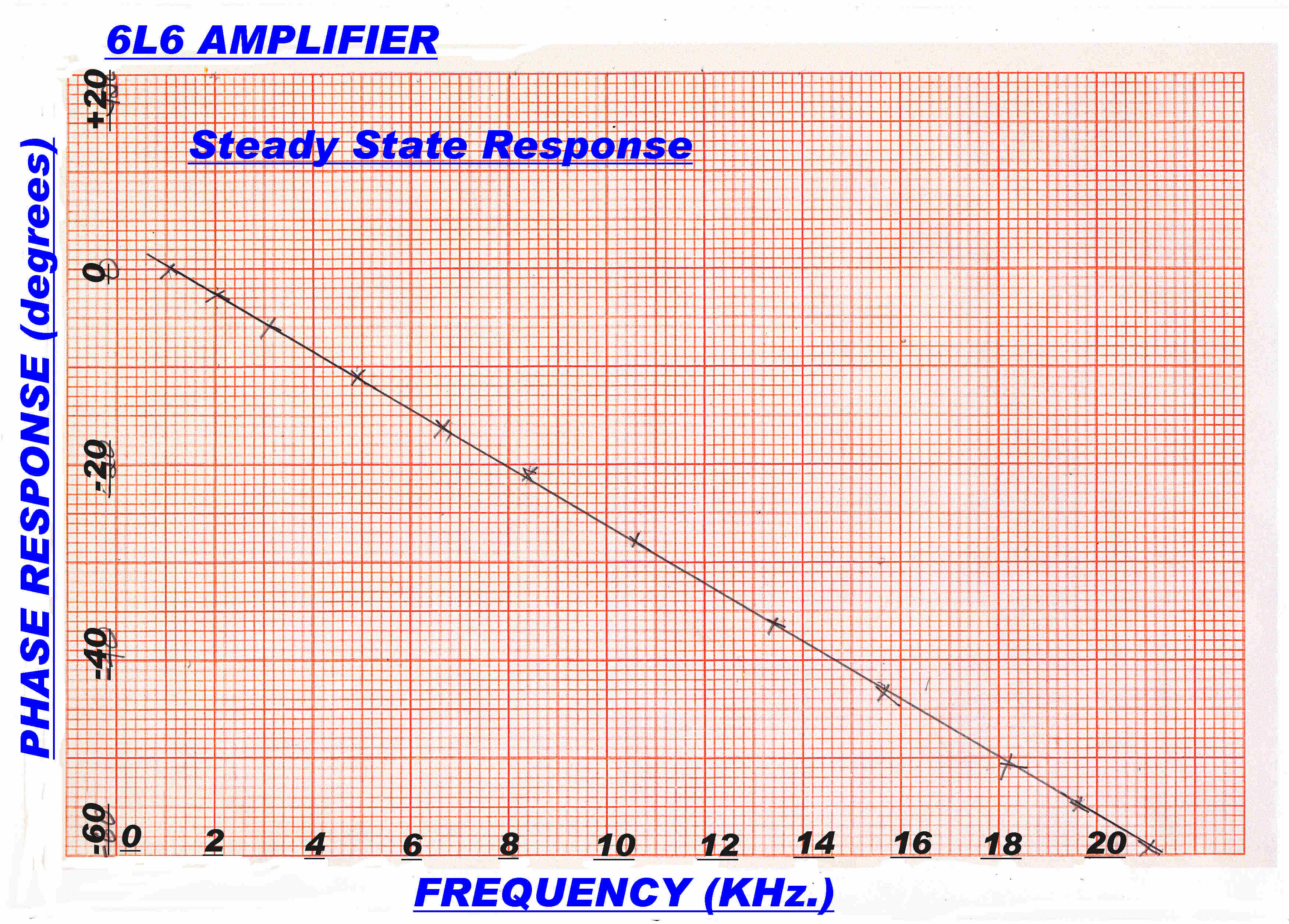
The steady state response should indicate that the amplifier
is flat and phase linear over the working frequency range.
The test results given below show that this has been achieved.
|
|
|
Amplitude Response |
Phase Response |
The distortion is at the limit of the test equipment.
New gear has been designed to extend the limit by several orders
of magnitude.
The distortion level is way below audibility, so the results are of
interest to confirm the design ideas but little else.

|

|

|

|

|

|

|

|

|
|
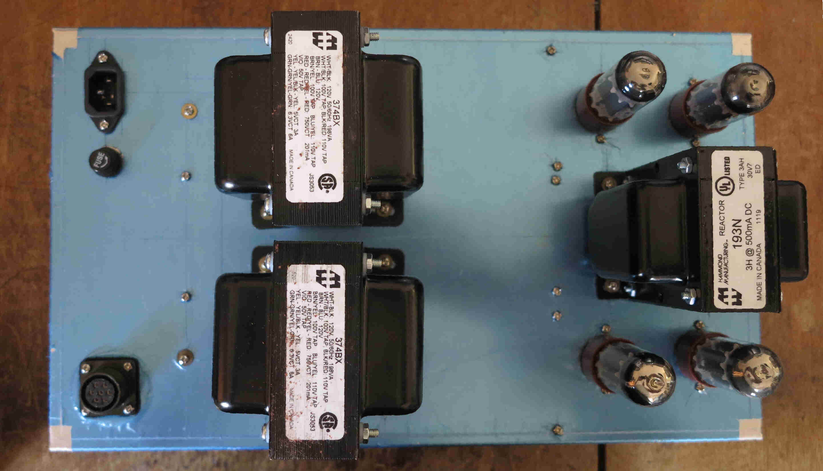
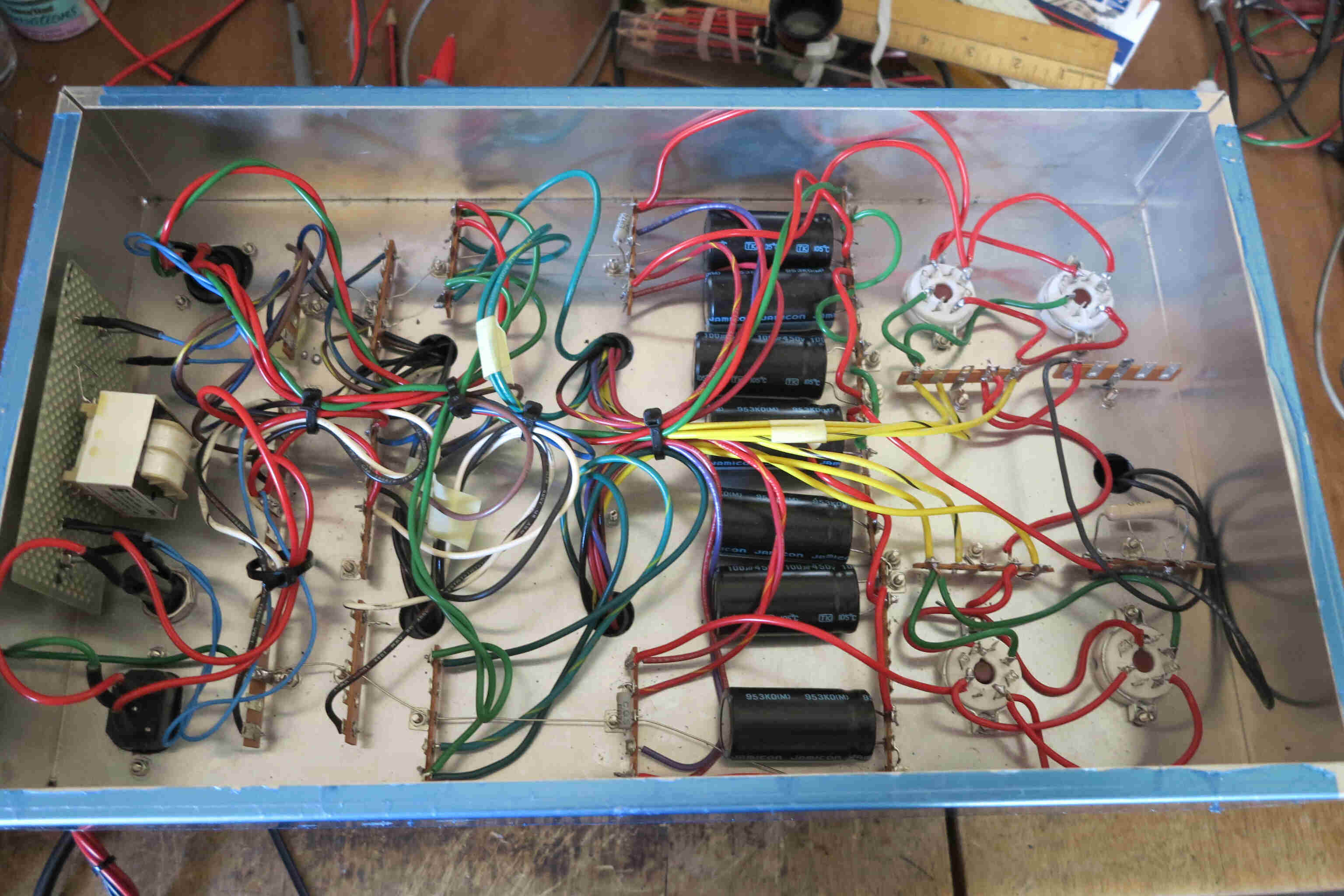
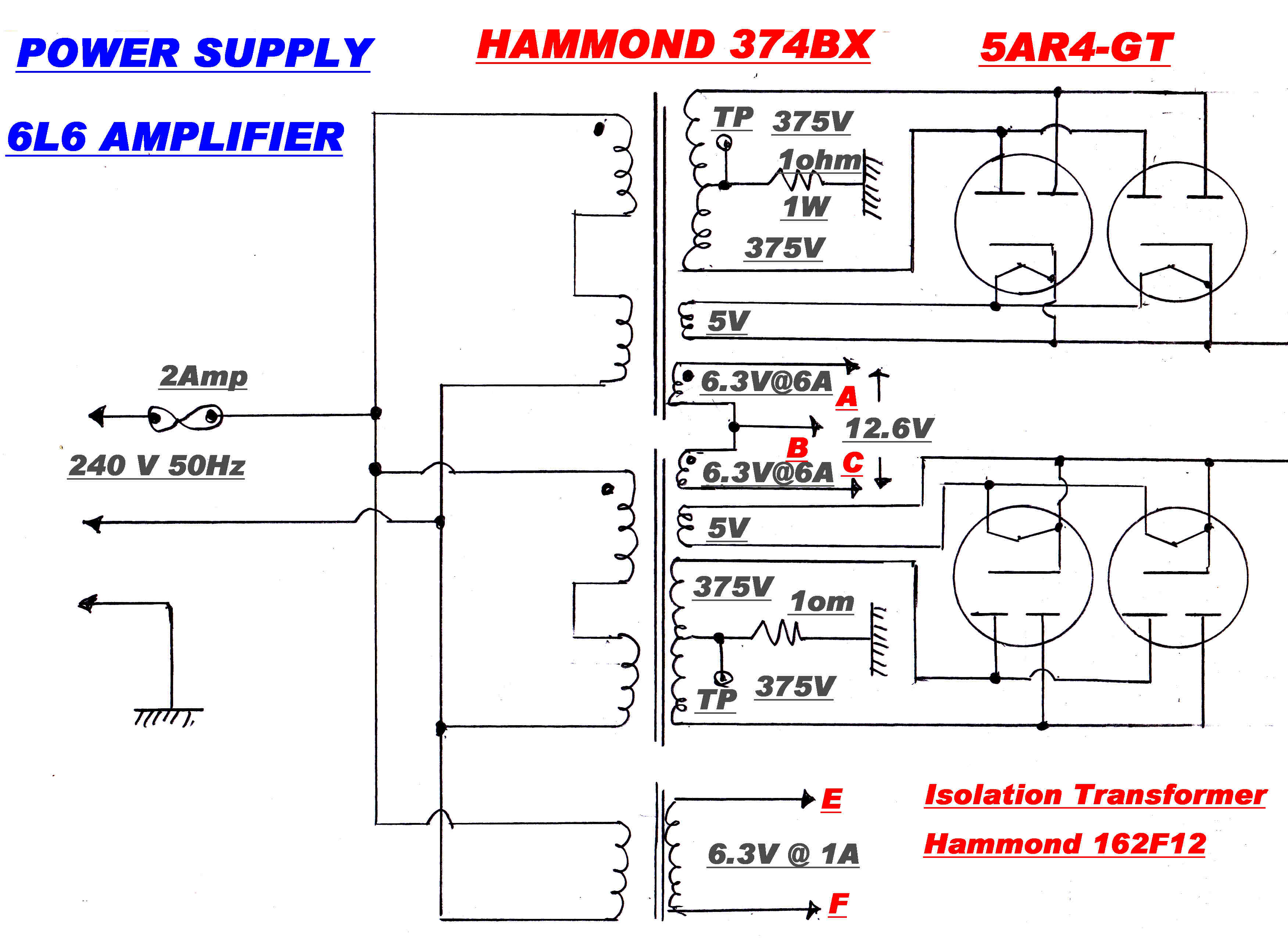
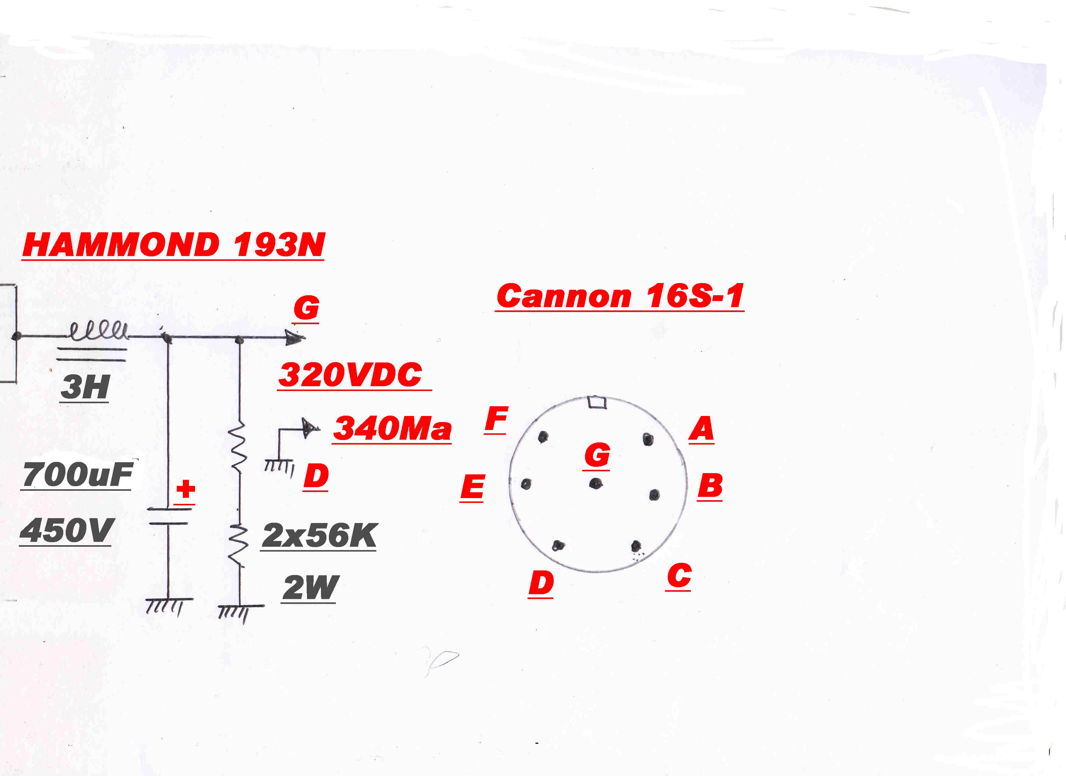
The circuit of the power supply for the vacuum tube amplifier is shown below.
|
|
BASIC DESIGN
An ideal class A push-pull amplifier presents a constant load to the power supply.
Because of the three halves power law, there is an increase in output stage current as
the output from the amplifier increases.
The heavy current feedback on the output stage, together with
the unbypassed cathode resistor, greatly reduce this increase,
so the load is practically constant regardless of power output.
Output voltage Vo = 320 volts: Load current IL = 0.38 amps:
RL = Vo / IL = 320/0.38 = 842ohms.
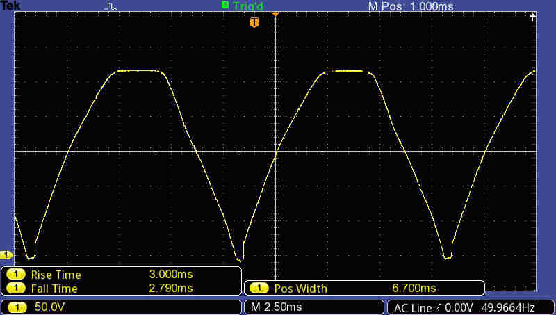
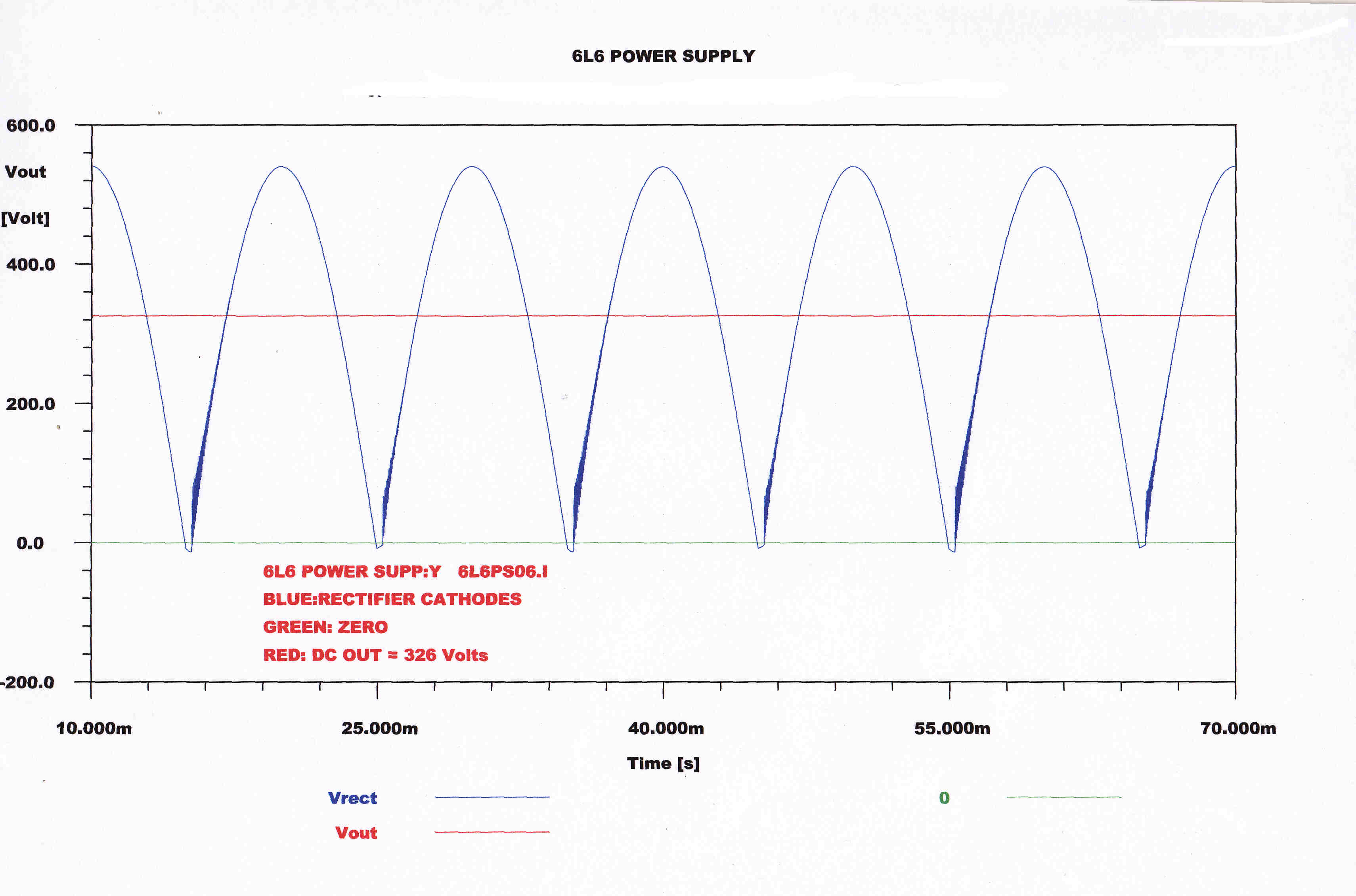
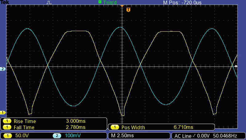
The measured and computed voltage on the rectifier cathodes is shown below:-
|
|
|
MEASURED VOLTAGE ON RECTIFIER CATHODES |
COMPUTED VOLTAGE ON RECTIFIER CATHODES |
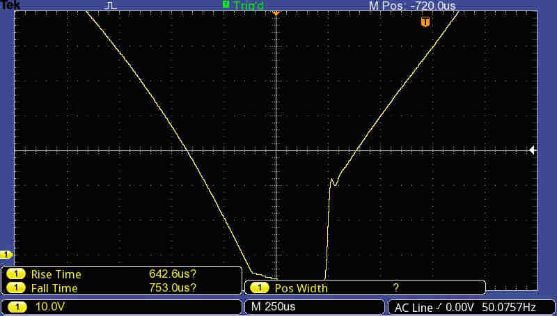 The leakage inductance of the power transformer limits the rate of rise of current
in the transformer secondaries when the full load current is commutated between windings.
For a short period the common cathodes go negative.
The resulting transient is shown opposite.
The Y scale is 20 volts/division.
Zero DC is at -2 divisions.
FILTER
 A choke input filter (with sufficient inductance) produces rectangular
current pulses of half cycle duration in the rectifiers.
The total current pulse on one side of the rectifier is shown opposite.
A capacity input filter produces short current pulses of high peak current.
Since the RMS value of the rectangular pulses is much less than that of the short high current
pulses, a choke input filter results in much less dissipation in the rectifiers
and transformers.
It is therefore highly desirable and greatly extends the life of the
rectifiers and transformers.
The capacity input filter gives a higher output voltage and lower ripple,
and so finds a place in non-profrssional gear.
This power supply has been intentionally over-designed to give reliability and long life.
The transformers run warm to the touch, and the peak repetetive rectifier cathode
current is 125Ma.
The peak repetetive rectifier cathode current allowed for the 5AR4 is 825Ma.
CRITICAL INDUCTANCE
A minimum value of inductance called the critical inductance is required
to prevent the rectifier from acting as a capacity input rectifier.
This inductance LC is given by:-
LC = RL/[ 6 Π f ]
Here RL = 842: f = 50 : so LC = 0.894H
Choose 3 H -- well above the critical value.
OUTPUT RIPPLE
When the inductance is above critical, the output waveform from
the rectifier is a full wave rectified sinusoid.
This can be expanded out in a Fourier series to give:-
v(t) = Vp[ 2/Π - 4/Π ∑ (cos( k ω t ))/( k + 1 )( k - 1 ) ]
for k even: k ≠ 0
Because the ultimate slope of the L-C filter is 12db/octave, the only significant
frequency in the output ripple is 100Hz.
The L and C components in the filter of a power supply usually have a fairly high
tolerance, so approximate calculations for output ripple are appropriate.
For instance, the inductance is quoted as 3H with a DC current of 500Ma. At 380Ma the
inductance is probably higher and furthermore non-linear.
Secondary Output Voltage Vrms = 375V
So Vp = √2 Vrms : Vp = 530V
where Vp is the peak voltage neglecting the small rectifier voltage drop.
From the expansion above with k = 2, K = 4/[3 Π ]
where K = Vsec/Vfund = 0.4244
The peak value of the second harmonic on the cathodes of the rectifier Vsec
is then given by:-
Vsec = 530 x 0.4244 = 225 volts
When the capacity C forms a simple voltage divider with the inductance of the choke L.
The attenuation A is given by:-
A = [ 1/i ω C ] / [ 1/i ω C + i ω L ]
Then A = 1/[ 1 - ω2 L C ]
First Caculation
In the first condition there was 600uF in the power supply and a further 22uF bypass in the amplifier.
Giving C = 622uF : L = 3H : f = 100Hz.
A = 1.3559 x 10⁻³ : Vpeak = 225
So Vpeak ripple = 0.3V
Second Calculation
In the second condition there was 700uF in the power supply and a further 22uF bypass in the amplifier.
Giving C = 722uF : L = 3H : f = 100Hz.
A = 1.171 x 10⁻³ : Vpeak = 225
So Vpeak ripple = 0.263V
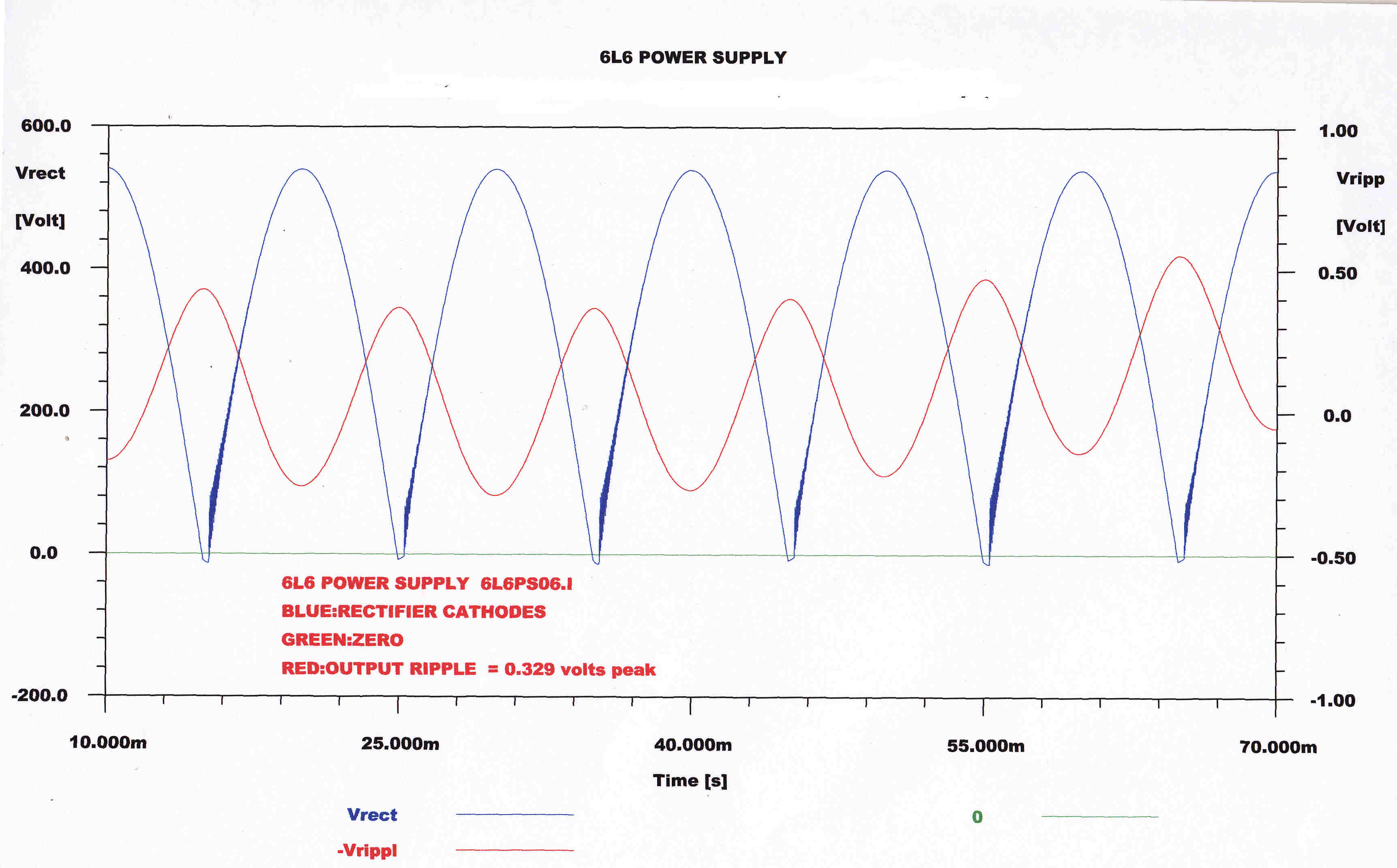
The measured and computed ripple is shown below.
|
|
|
MEASURED RIPPLE ON OUTPUT |
COMPUTED RIPPLE ON OUTPUT |
CHOICE of THERMIONIC RECTIFIER
A diode with an indirectly heated cathode (5AR4-GT) is much more desirable than
those ( 5Y3, 5Z4, 5AU4, 5AS4 ) with filamentary cathodes.
(1) The dimensions are under tighter control, so the tubes can be manufactuured with
smaller plate cathode spacing giving a lower voltage drop.
The reduced plate cathode spacing makes the tube more prone to reverse breakdown during
transients.
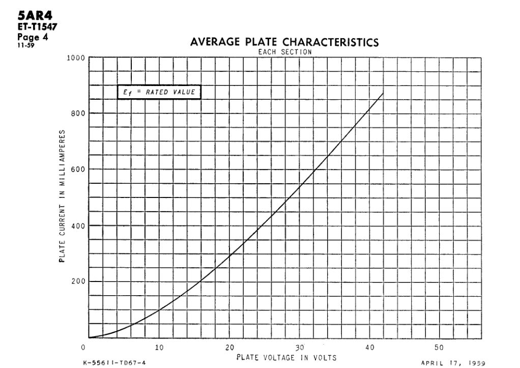
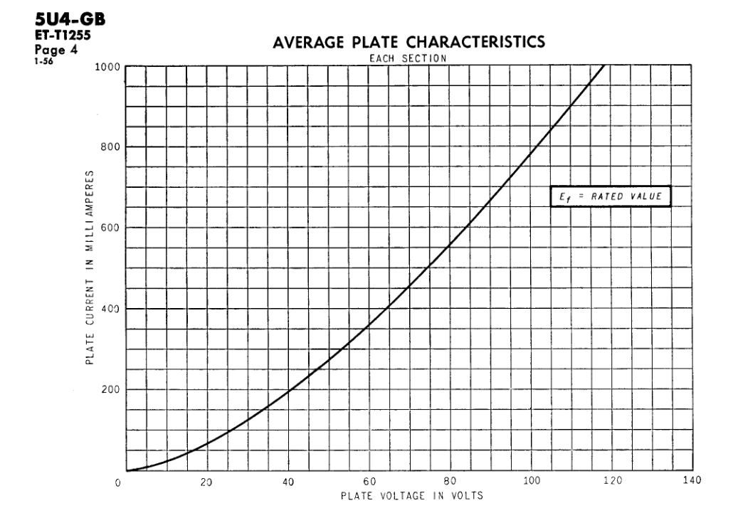
For For a plate voltage of 16 volts the plate currents are:-
5AR4 .... 200Ma
5AS4- 5U4 .... 50Ma
The plate characteristics of both tubes is shown below.
(2) The thermal time constant of a filamentary cathode is much less than that
of an indirectly heated cathode. This means that the B+ high tension rail comes
up to full voltage before emission begins in the amplifier tubes.
Since the load presented by the amplifier is very high, the inductance is
below critical, and so the high tension reaches the peak output voltage from
the secondary of the transformer. (530V)
Further, a significant fraction of this starting transient is applied to
the grids of the amplifier tubes via the load resistors and coupling capacitors.
This produces an intense electric field at the surface of the cathode
as emission starts.
It is claimed that this reduces the life of the cathode.
With modern frame grid tubes such as the ECC88/6DJ8 the field is sufficient to cause
break down ( probably due to field emission) and the tube is destroyed.
To prevent this small neon tubes are placed between the grid and cathode.
|
|
|
5AR4 PLATE CHARACTERISTICS |
5AS4 PLATE CHARACTERISTIC |
HOT SWITCHING
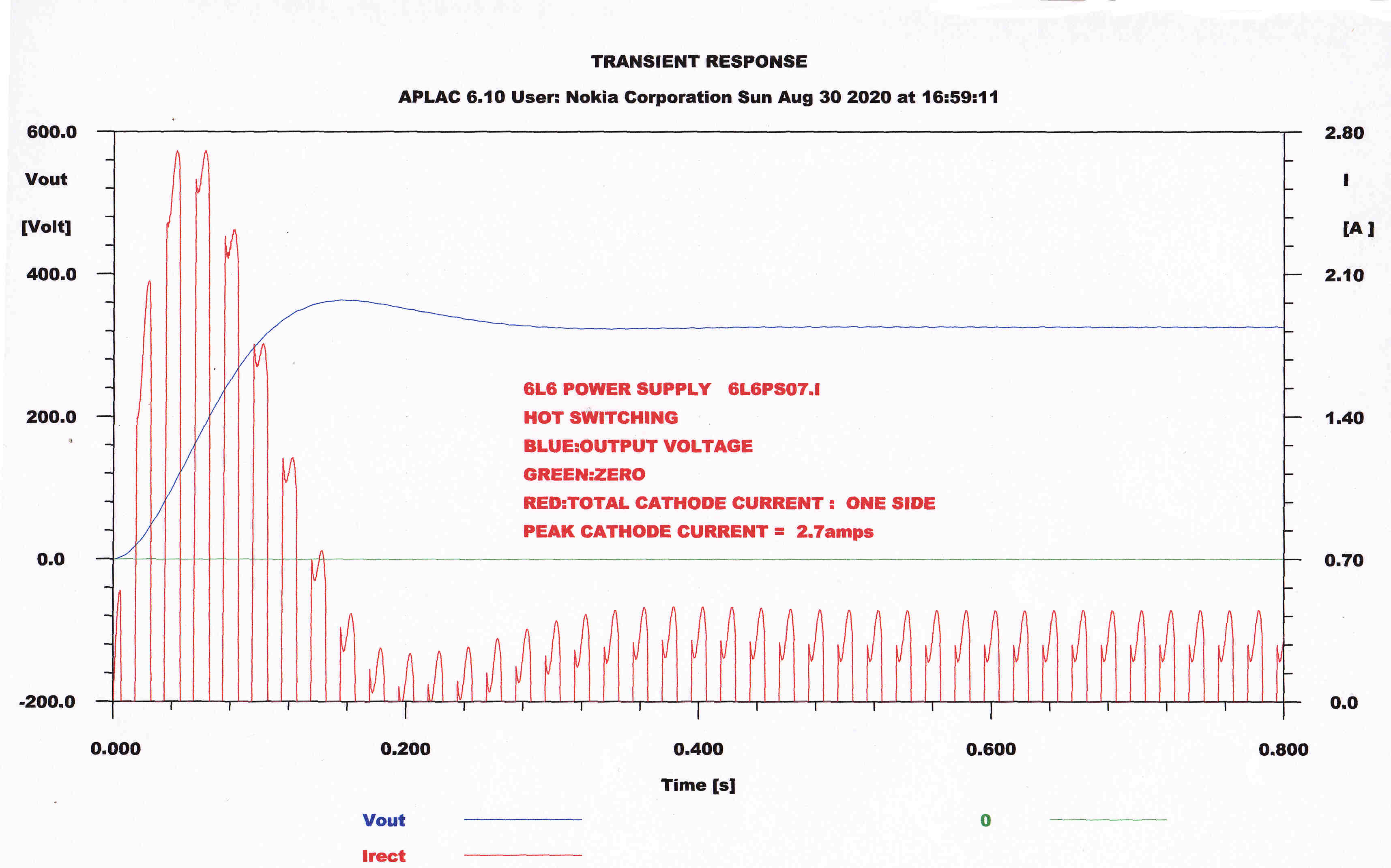 The momentary disconnection of mains voltage from a power supply can lead to
dangerous conditions.
The thermal time constant in the cathode maintains emission during the transient.
In a capacity input rectifier full mains voltage is suddenly applied to the capacitor.
The switching transient current can be large and destructive, and is limited only by the output
impedance of the transformer and the rectifier voltage drop.
A choke input filter greatly reduces the peak value of hot switching transients.
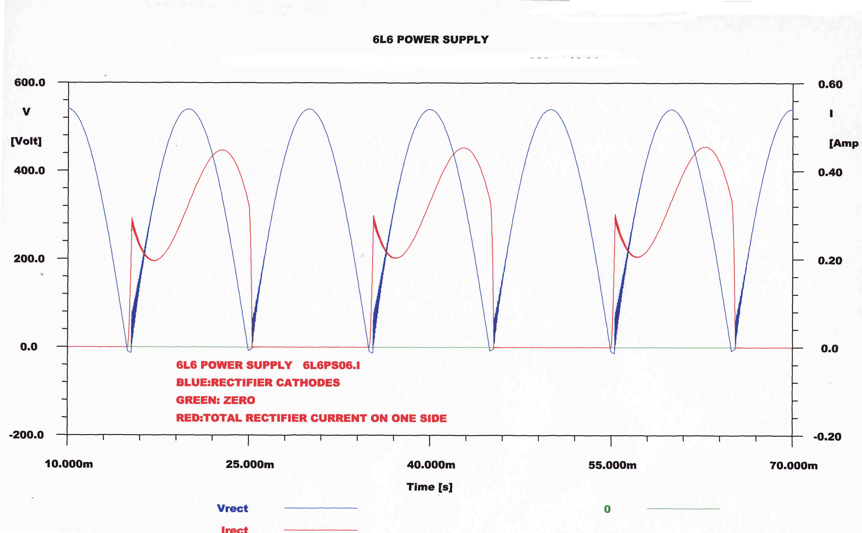
A computer solution for the worst case of hot switching is shown.
Blue: Output Voltage Transient
Red: Total Rectifier current on one side.
The total peak rectifier current is about 2.8 amps - giving a peak current for each rectifier
of 0.7 amps. This is within spec for the 5AR4 - demonstrating the safety of a choke input rectifier.
FILAMENT SUPPLY
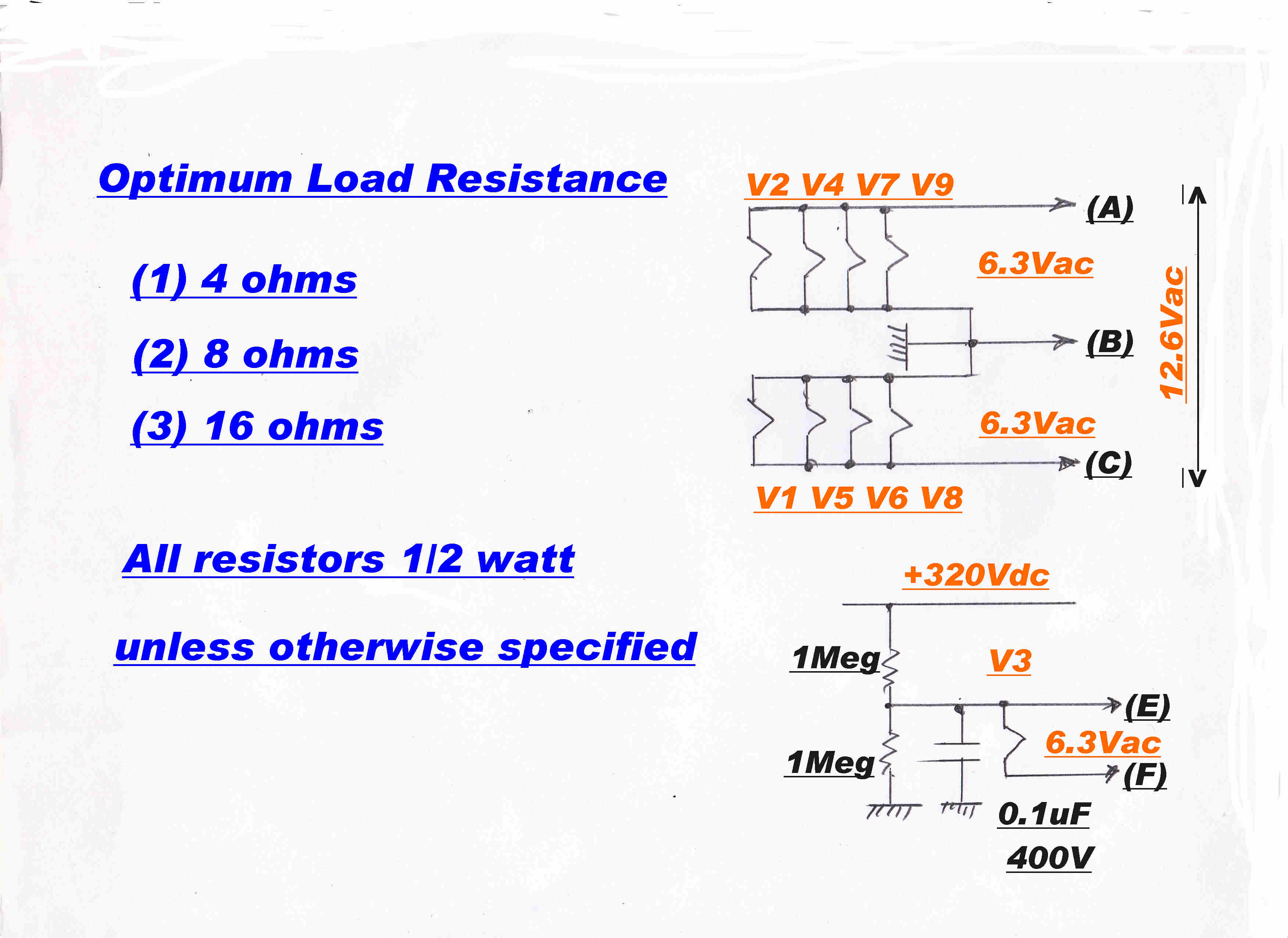
The main filament supply is arranged so that it is effectively 12.6 volts
rather than 6.3 volts. This reduces voltage drop in the connecting lead.
The filament supply is earthed only at the amplifier to prevent circulating currents and hum.
Two cathode followers in the amplifier have their cathodes raised to about 150 volts DC.
A floating filament supply is raised to this DC level to minimise the cathode to filament
voltage. Most tubes can operate with a cathode - filament
potential difference of 150 volts, but it is good practice to reduce it.
TURN OFF TRANSIENT
Standing currents in inductors produce transients at turn off.
[A] Turn off may occur when the magnetising current in the transformer primary is at a maximum.
This can cause very high reverse voltage transients across one rectifier tube
in choke input filters, but not in capacity input filters.
[B] The transient caused by the full load current flowing in the filter inductor does not produce
large reverse voltages on the rectifier.
[A] An estimate of the order of magnitude of the transient due to switching
the magnetising current at its peak follows:-
Magnetic energy in the transformer core Em = 1/2 L I2
This is then dumped into the stray capacity across the primary C.
The energy stored in the capacity C across the winding Ee = 1/2 C V2
where I is the peak value of the magnetising current: V is the peak volltage transient
across the winding.
So Em = Ee
1/2 L I2 = 1/2 C V2
V = [ L/C]1/2 I
For the two transformers in parallel approximaate values are:-
L = 5.88H: C = 1nF: I = 0.255A so that the peak voltage across the primary Vpriis:-
Vpri = 19.6KV
This causes a peak voltage of Vpk across both ends of the secondaries where :
Vpk = (2 x 375)/240 x Vpri = 61KV!
The conducting diode pulls its cathode to the peak positive potential at one end of the secondary
and this full reverse voltage appears across the non conducting diode, since the filter inductor
can have little effect at the high ringing frequency fo = 20 8 KHz.
The addition of a 2uF capacitor across the primary reduces the peak value of the transient voltage
Vpri to a safe value.
Here L = 5.88H: C = 2uF: I = 0.255A so that Vpri = 437 volts.
In a capacity input rectifier, all the primary magnetic energy is dumped into the first capacitor.
Because of its size, the capacitor voltage rises very little from its DC value Vo, say, 300
volts and clamps the voltage across the transformer.
The change in capacitor voltage Δ V is given by:-
ΔV = [1/2][ L/CVo][ I^2]
If C = 350uF and Vo = 300 V , Δ V = 1.8 volts.
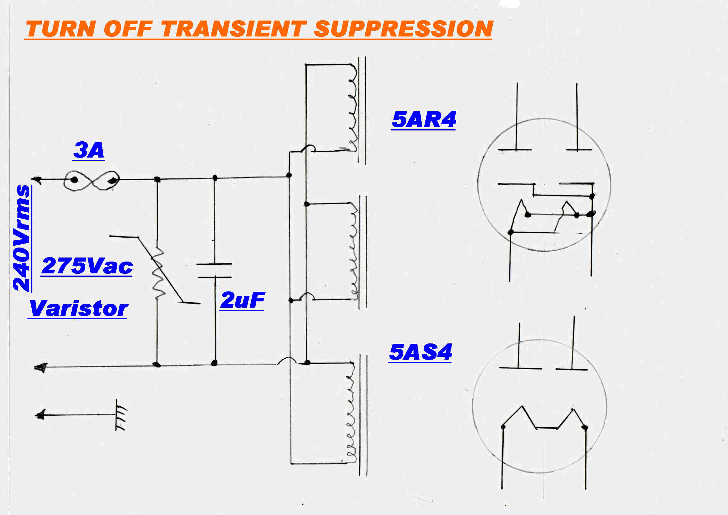 Modifications to the power supply to suppress transients are shown opposite.
On turn off the peak magntising current is diverted into the 2uF capacitor to produce a peak
voltage of 437 volts and a ringing frequency of 464 Hz.
A mains voltage varistor is added for further protection from mains transients.
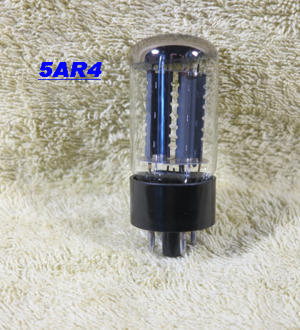
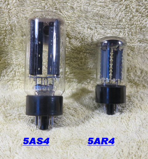
The detailed internal connections of the 5AR4 and and 5AS4/5U4 rectifier double diodes is also shown.
SUBSTITUTION OF THE 5AS4 FOR THE 5AR4
The 5AS4 may be plugged directly into an octal socket wired for the 5AR4.
This results in a small reduction of the B+ 320 volt high tension rail with a ccorresponding reduction of
peak power output.
The AC filament voltage in the 5ASR will either add or subtract from the AC plate voltage depending on the
random phasing of the transformer connection.
The filament connected to pin2 has more disturbing voltage than the side connected to the output pin, pin 8.
This causes some unbalance in the two diodes.
In amplifiers designed specifically for the 5AS4 diode balance is achieved by taking the output from a centre tap
on the 5 volt filament winding.
The peak current through each diode is about 120MA. , so the voltage drop in the 5AS4 is sbout 28
volts, and this tends to mitigate against the unbalance due to the small filament voltage.
The voltage drop across the 5AR4 is about 11 volts.
|
|
|
|
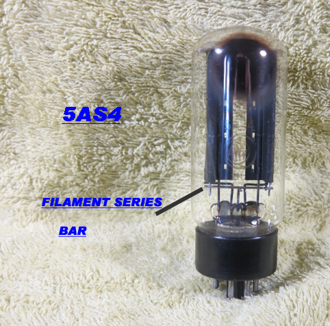
A bar connects the two filament cathodes of the 5AS4 in series. |
The heaters and unipotential cathodes of the 5AR4 are connected in parallel. |
The relative size of the 5AS4 and 5AR4. |