VACUUM TUBE AMPLIFIER

CONTACT : COMMENTS AND QUESTIONS
back/home
Many designs for vacuum tube audio amplifiers have been published.
It is rare to find a detailed description of the thought processes pursued during the
evolution of the design and a detailed account of the reasons for adopting
a particular circuit topology.
This section is an attempt to correct this deficiency.
It is purposely made discursive and somewhat repetitive in the hope of recording,
in some detail, the now rather arcane process of vacuum tube design.
The design is not realised with modern vacuum tubes, but with old friends --
6SN7:6SJ7:6AC7:6V6 -- tubes I used in some of my earliest designs, and all of which
were available by 1938.
Why vacuum tubes?
Because they are beautiful, and because virtually all circuit techniques
were established with them, not with solid state devices.
There are a couple of guiding principles in the design of vacuum tube
equipment:-
(A) The overall performance should be made as independent as possible of the
characteristics of the vacuum tubes.
(1) STABILITY of TUBE OPERATING POINT [ OUIESCENT CURRENT]
The operating point of the vacuum tube should be stabilised by DC feedback:
usually from cathode bias resistors, but additionally with screen voltage
feedback in pentodes.
For instance, four output tetrodes in a push pull amplifier should not
share a common cathode bias resistor. Each should have its own individual
bias resistor to stabilise the plate current.
The initial balance during setup should then be maintained over long periods.
Any design which calls for "matched" tubes should ring alarm bells.
The tubes may not stay "mathced" for very long.
The above applies to vacuum tube pulse circuitry as well as linear circuits
such as audio amplifiers.
The gain in the DC feedback loop to stabilise the operating point of a tube increases
with the cathode bias resistor. Sometimes the grids of an AC coupled amplifier
are returned to a regulated voltage, say 25 volts, so the cathode resistor can
be increased to further stabilise the quiescent current.
This technique is found mostly in very high quality test gear such as:-
The Siemens Pegelmesser 3D 343 [Level Meter or Wave Analyser]
(2) INTERNAL FEEDBACK LOOPS
Internal and overall feedback can stabilise the gain and frequency response
of a vacuum tube amplifier.
With a large degree of feedback, these parameters can be forced to depend uniquely on
the ratio of two resistors - the ultimate goal in any design.
Feedback is useful only when the required bandwidth is a fraction of the maximum bandwidth
possible with any given tube.
This is the case in an audio amplifier or an AM transmitter with envelope feedback.
Here the maximum signal frequency is about 20KHz but the response is usually taken out to,
say, 10 times this --- 200KHz.
In a pulse amplifier, for instance the Y amplifier of an oscilloscope, overall feedback
makes the transient response a complicated function of gain. As this drifts, so does
the all important transient response - most undesirable in test gear dedicated to
waveform measurement.
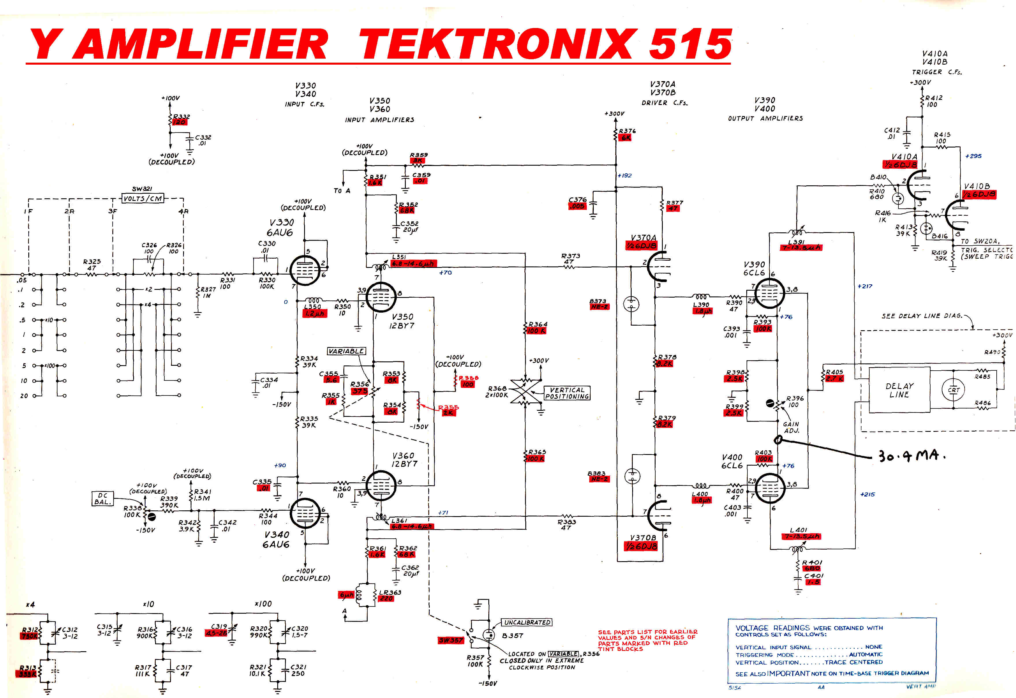
No feedback therefore is found in Tektronix Oscilloscope vacuum tube Y amplifiers for
this reason. [ See CRO types 515 or 545A or plugin preamps types L or CA]
The total cathode current of pushpull stages in these amplifiers is stabilised.
The balance is controlled by feedback, but this is through the operator
setting the trace to the centre of the CRO screen.
The overall gain is also set by a "tweak" on the front panel - again feedback
via the operator.
The response time required of the X deflection amplifier is usually much slower
than for the Y amplifier. Here linearity is important to give a uniform time scale.
Negative voltage feedback is used on the X deflection amplifiers.
There are further complications with overall voltage feedback on Y amplifiers:-
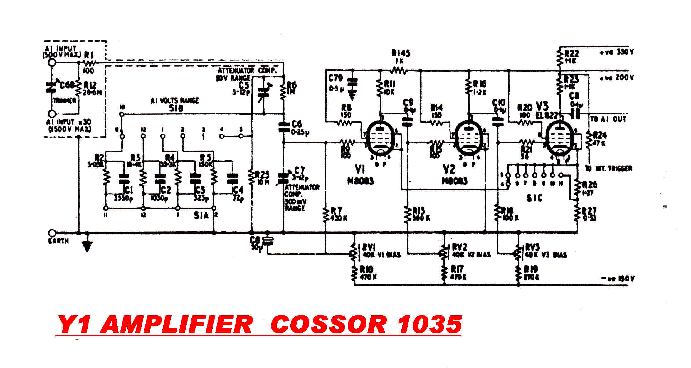
The Cossor model 1035 used voltage feedback on the Y amplifier.
Gain was changed by varying the degree of overall feedback and, with it,
the transient response. Waveforms which change their shape with gain setting
can be confusing.
While not exactly pertinent to the present discussion, it seems appropriate to
make the following point:-
Beware of trick circuits which use only one tube to do the job of many.
Their performance is usually unsatisfactory and they almost always are highly sensitive
to tube characteristics.
The time base in the Cossor 1035 CRO is a case in point. It used a "Phantastron"
Miller integrator to generate the time base.
Under some trigger conditions it ran backwards at the start of the trace.
The oscilloscope was widely used in teaching laboratories in the mid fifties.
The concept of negative time caused some consternation in the students.
The time base in the Cossor 1035 used three tube functions: the time base in
the competing Tektronix 515 used sixteen.
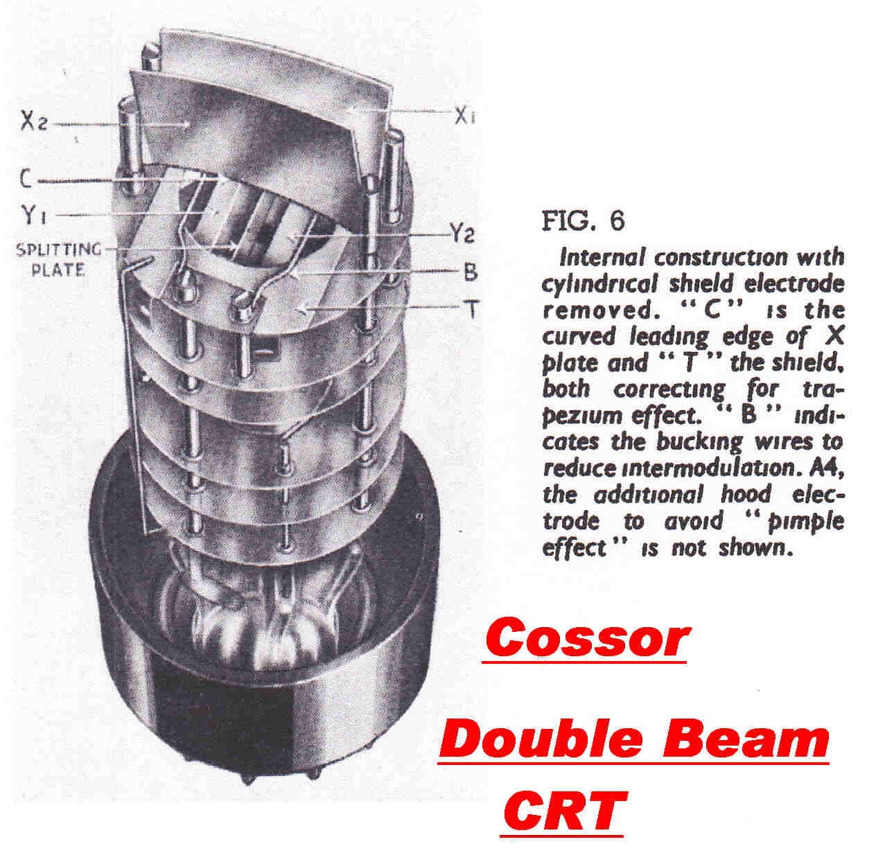
To be fair, the cathode ray tube used in the 1035 Cossor was a masterpiece of design.
The beam was split in two by an intersecting plate to give a genuine double beam oscilloscope.
The geometry then dictated that deflection was by a single active plate and an earthed plate.
An asymmetrical deflection system like this gives rise to trapezoidal distortion.
This was cleverly corrected in the tube.
There is a further complication when negative voltage feedback is used on
amplifiers - NEGATIVE INPUT CONDUCTANCE.
In a typical amplifier the input signal is on the grid of the first tube and
the feedback appears across a resistor in the cathode.
The phase change in the amplifier at high frequencies causes a leading voltage
to appear across the grid cathode capacity of the tube.
The resulting current through the input capacity has a component 180
degrees out of phase with the input voltage - a negative input conductance.
The possibility now exists that any inductor of reasonable Q hung across the input
terminals will resonate with the input capacity and burst into oscillation.
Such a condition existed in the Cossor model 1035. It was a great shock
to many students to see passive networks apparently burst into
spontaneous oscillation.
The condition was by no means confined to Cossor oscilloscopes.
The AC voltage sensing amplifier of the HP 3465A digital voltmeter has a negative input
conductance between 46KHz and 150KHz on the 200mV range.
When a 17.2 mH inductor is connected across the terminals, a 0.7V peak sinusoid
at 60KHz appears.
The AC measurements made with this voltmeter therefore have to be taken with caution.
Even single stage feedback amplifiers can develop a negative input conductance.
A cathode follower with a capacitance load is a good example.
|
|
|
|
The cathode current in the six cathode followers and the two push-pull
amplifying pairs is stabilised by returnig the cathodes to a negative voltage. |
The amplifier is AC coupled, so one of the most significant components of
the input is lost. Further, any DC on the input causes a large transient when the
signal is applied to the input. |
The undeflected beam is intersected by an earthed plate which splits it in two. |
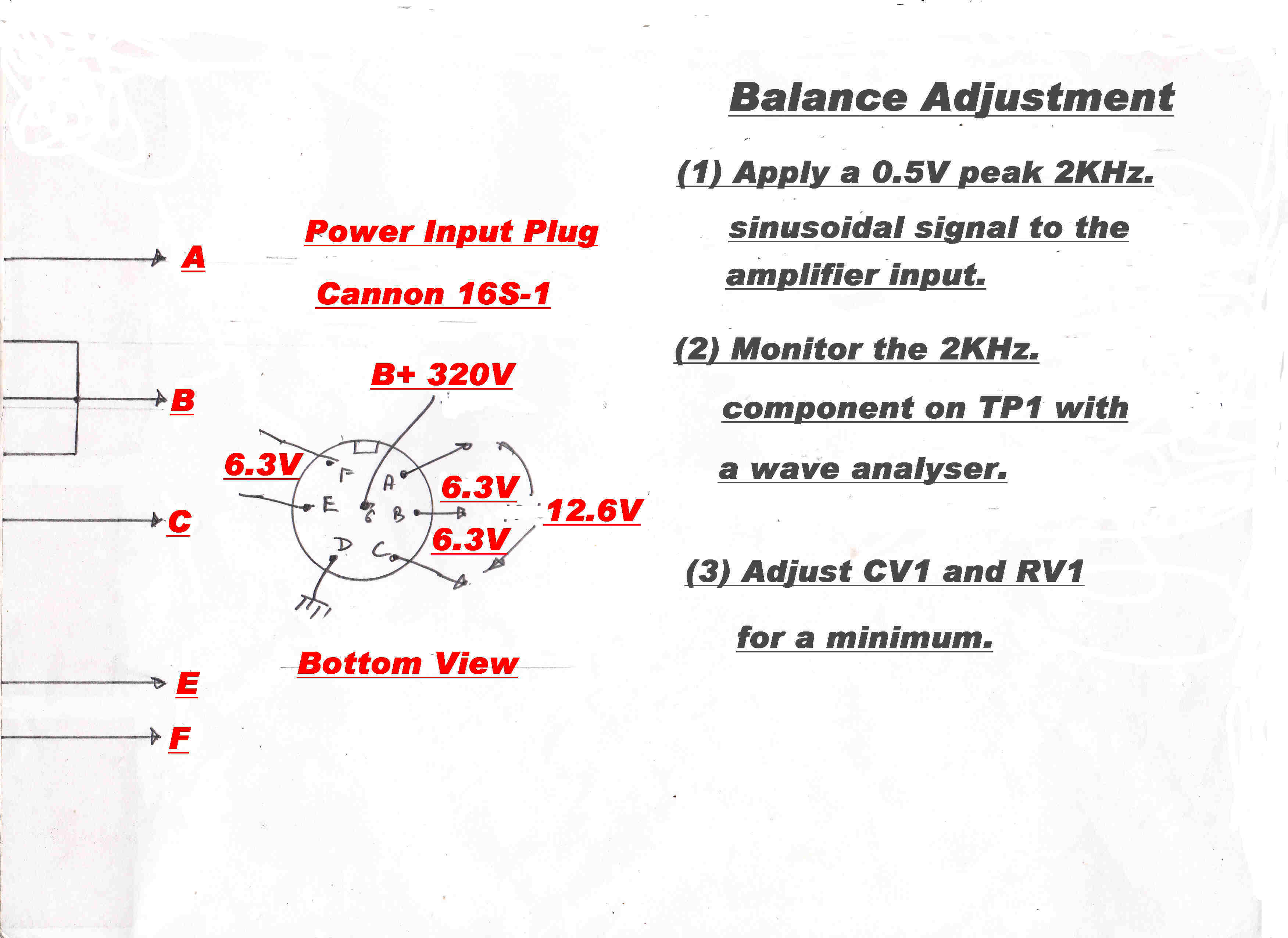
(B) Preset Adjustments Should be Orthogonal
During initial setup it may be necessary to adjust parameters such
as current balance in an output stage.
For rapid convergence it is highly desirable that these adjustments do
NOT interact - that is they are orthogonal.
It is also highly desirable that the required condition results in some signal
going to zero.
For instance, in the audio amplifier described below, there is only one initial tweak -
to balance the current swing on either side of the push pull output stage.
A non-interacting variable R and C are adjusted for zero voltage across a 1 ohm resistor.
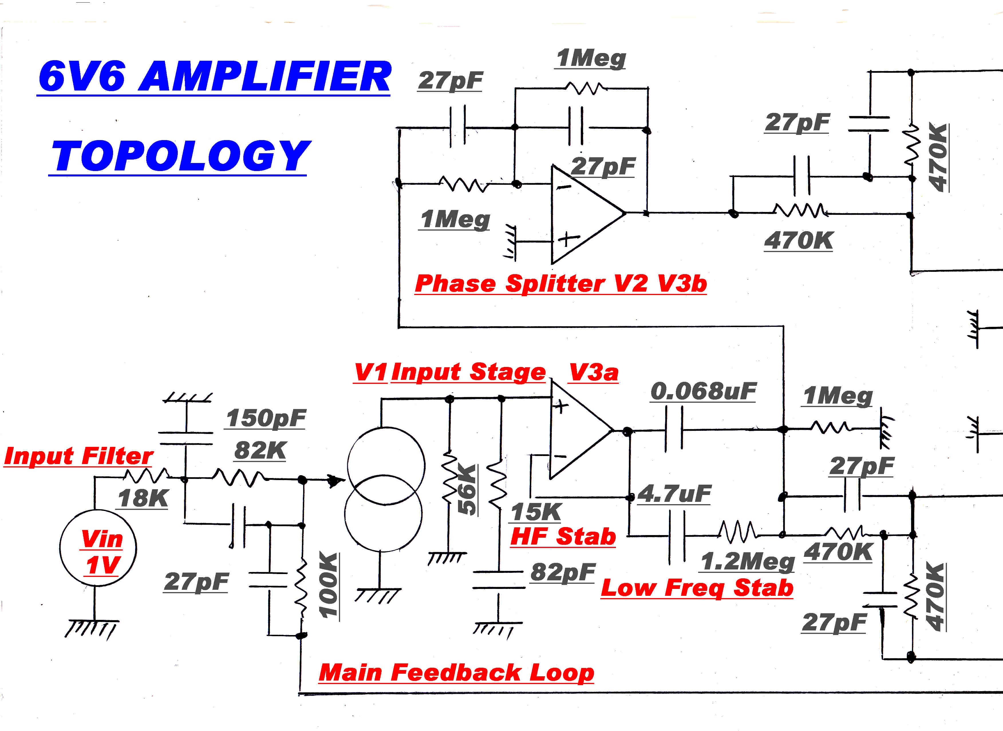
An outline of the 6V6 amplifier topology is shown below.
Also see the 6L6 Amplifier Topology
|
|
GENERAL COMMENT ON THE 6V6 AMPLIFIER TOPOLOGY
Many push-pull vacuum tube audio amplifiers have symmetrical feedback loops taken
from either side of the primary of the output transformer.
Analysis and experience show that this increases the amplifier sensitivity to component drift and
is to be avoided.
Internal feedback loops on one side of the amplifier must not be influenced by a signal on the other side.
Here the internal feedback loop is taken from the cathode of the output pentodes, so that it is not influenced by
conditions on the opposite side of the amplifier.
The plate current of the pentode stage produces the output signal, but the cathode current is the sum of the screen
and plate current which have a non-linear relationship at low plate current.
The screen current is therefore subtracted from the cathode current to produce a feedback signal representing the plate current
of the pentode output stage.
Heuristically, a push-pull tube amplifier may be considered as two amplifiers in parallel.
Voltage feedback from either side of the primary lowers the output impedance of both amplifiers , so that they tend to become
voltage generators.
Small variations in paralleled voltage generators produce large variation in load sharing, and so asymmetry between the sides.
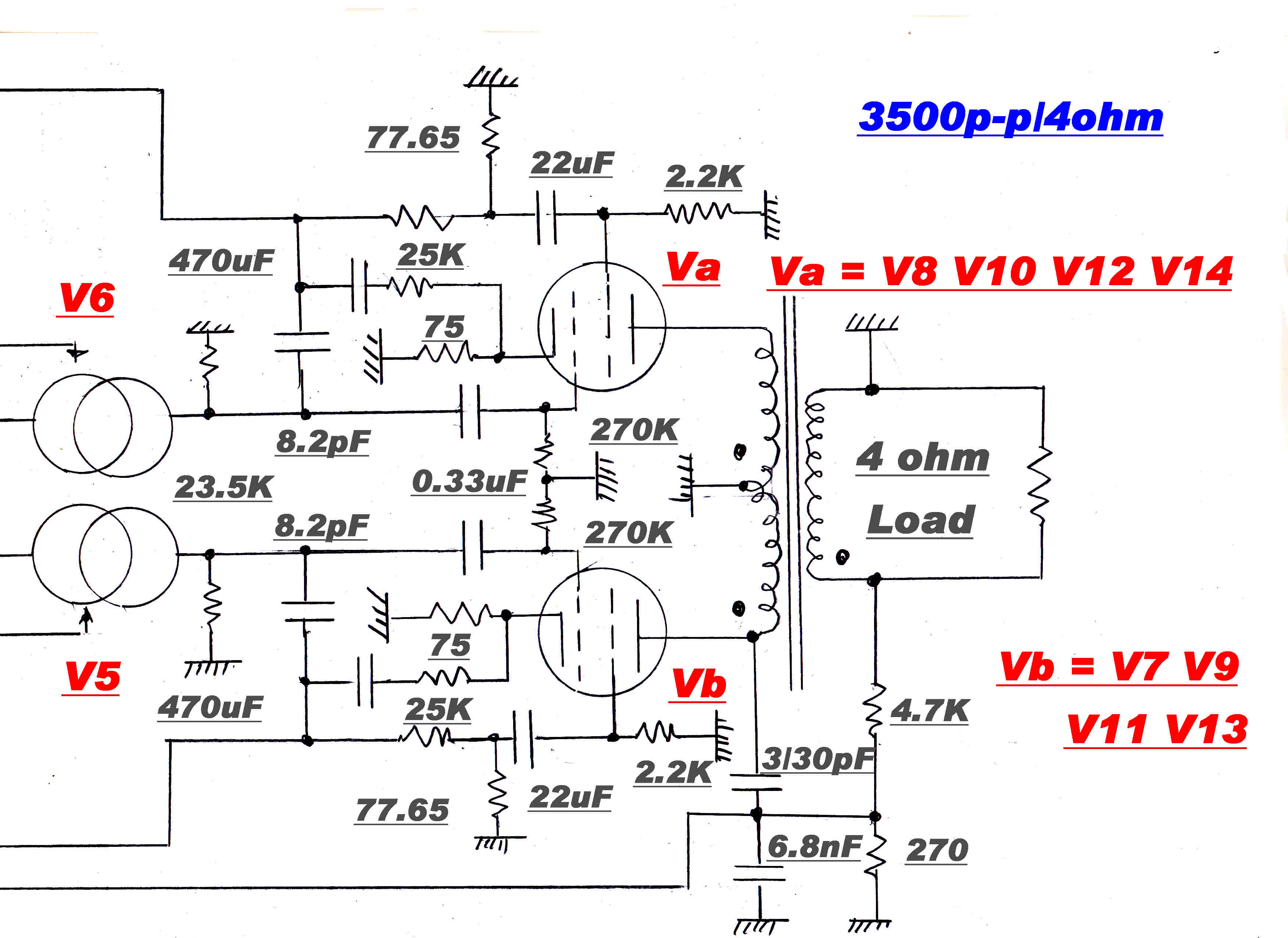
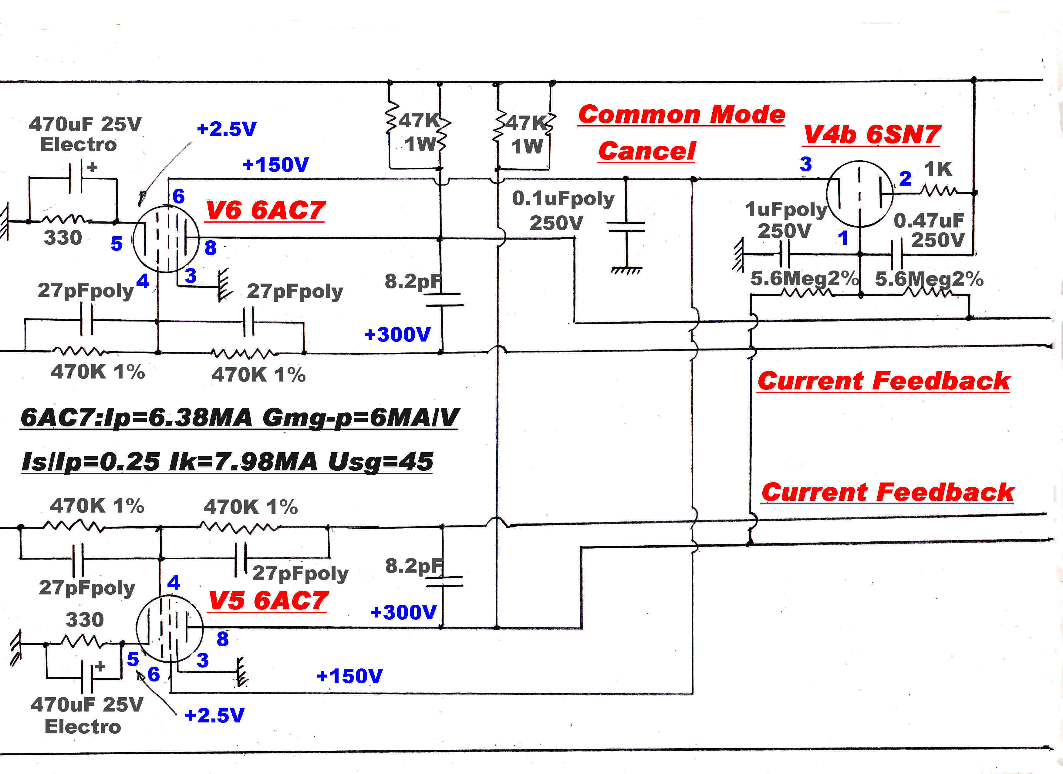
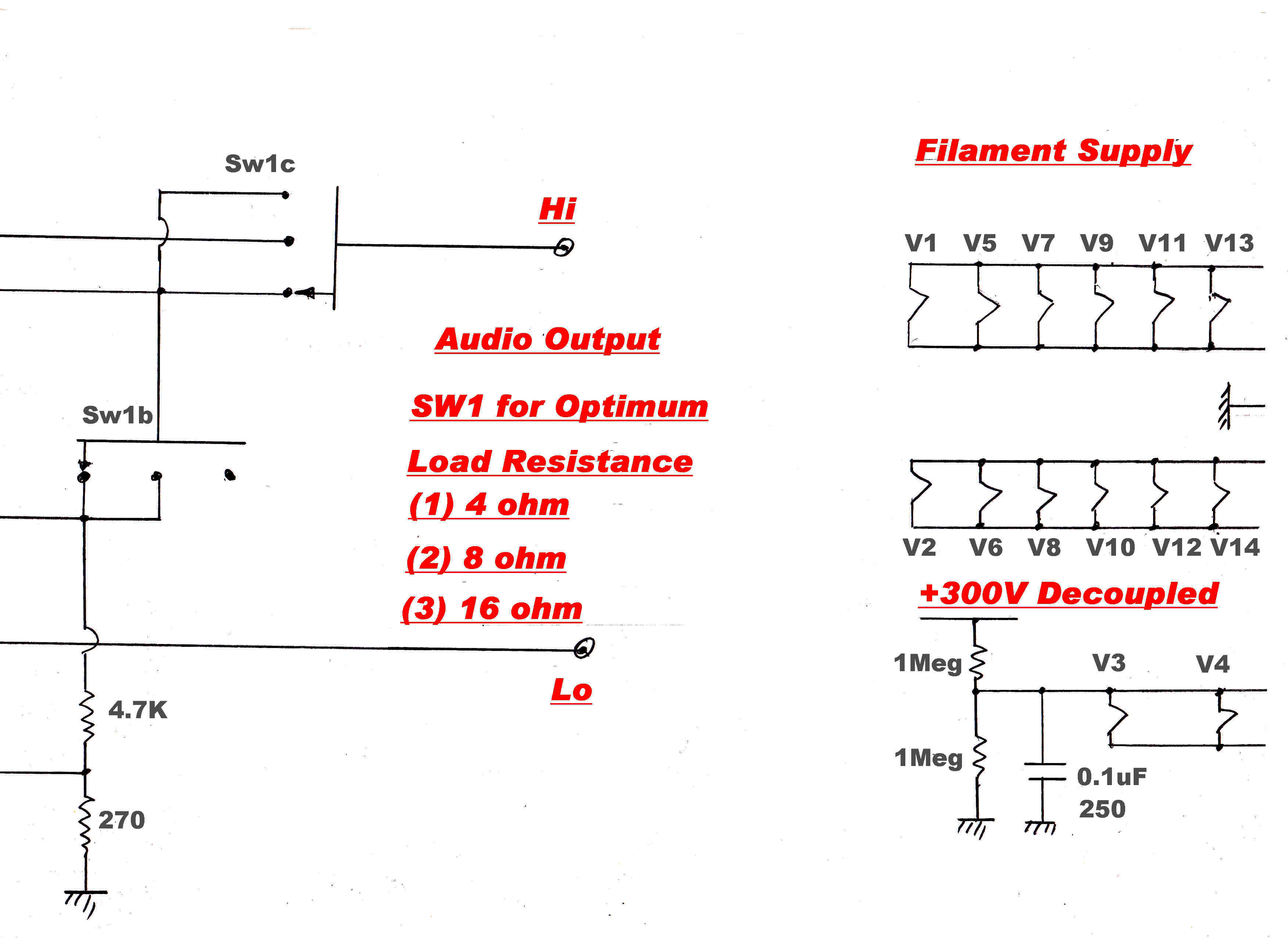
OUTPUT STAGE PLATE CURRENT FEEDBACK
The total cathode current [ Iplate + I screen ] is sensed by the 75 ohm cathode resistor. This
is made up of the four 300 ohm resistors in parallel.
The total screen current [ Iscreen] is sensed in the 77.65 ohm resistor. This, in parallel with the 2.2K screen feed resistor, gives an output
resistance of 75 ohms.
An increase in cathode current causes the voltage to go positive: an increase in screen current causes the voltage to go negative.
The junction point voltage of the two 25K resistors [ 4 100K in || ] then represents the DIFFERENCE betwen the cathode and screen current
- that is the plate current.
The error signal between the demand from the input stage and the plate current of the output stage [6V6] appears at the junction
of the 470K resistors at the inputs of the current generators V5 and V6 [6AC7s].
Note: The feedback must be generated by the plate current, not the cathode current, since it is the plate current
which produces the output signal.
The high Gm of the current generators [6AC7] produces a large gain across the 23.5K load resistors.
This gives over 20db of feedback over the plate current of the output stage.
This has two results:-
[A] The distortion in the output stage is reduced by more than a factor of 10.
[B] The gain of th output stage is stabilised against drift in output tube characteristics, so that the balance in the push-pull amplifier will
remain fixed for long periods.
Individual cathode resistors in the 8 6V6 output stages help stabilise the quiescent current of each tube.
Matched tubes are not required.
STABILITY OF THE FEEDBACK CURRENT LOOP
There are two high frequency poles in the forward path of the current loop:-
(1) One is formed by the input capacity of the 6V6 output tubes across the 23.5K drive resistor:
(2) The other by the capacitive loading of the 25k feedback resistors by the 27pF across the resistive divider in the input
to the current generator.
The effects of this second pole are removed by the 8.2pF bypass capacitor.
INPUT LOW PASS FILTER
The 18K resistor and 150pF capacitor form a low pass filter on the input to the amplifier.
It prevents RF from entering the input stage of the amplifier while keeping the cutoff frequency
well above the audio range.
It also makes the transfer function of the feedback network independent of the driving point impedance
into the input terminals of the amplifier. In other words, the device driving the amplifier cannot upset the stability.
STABILISING NETWORKS
The 15K - 82pF across the 56K load on the input current generator V1 [6SJ7] produce a shelf to improve
the phase margin in the high frequency overall feedback loop.
The 1.2Meg - 4.7uF across the 0.068uF coupling capacitor increase the phase margin, and so the stability,
of the low frequency loop.
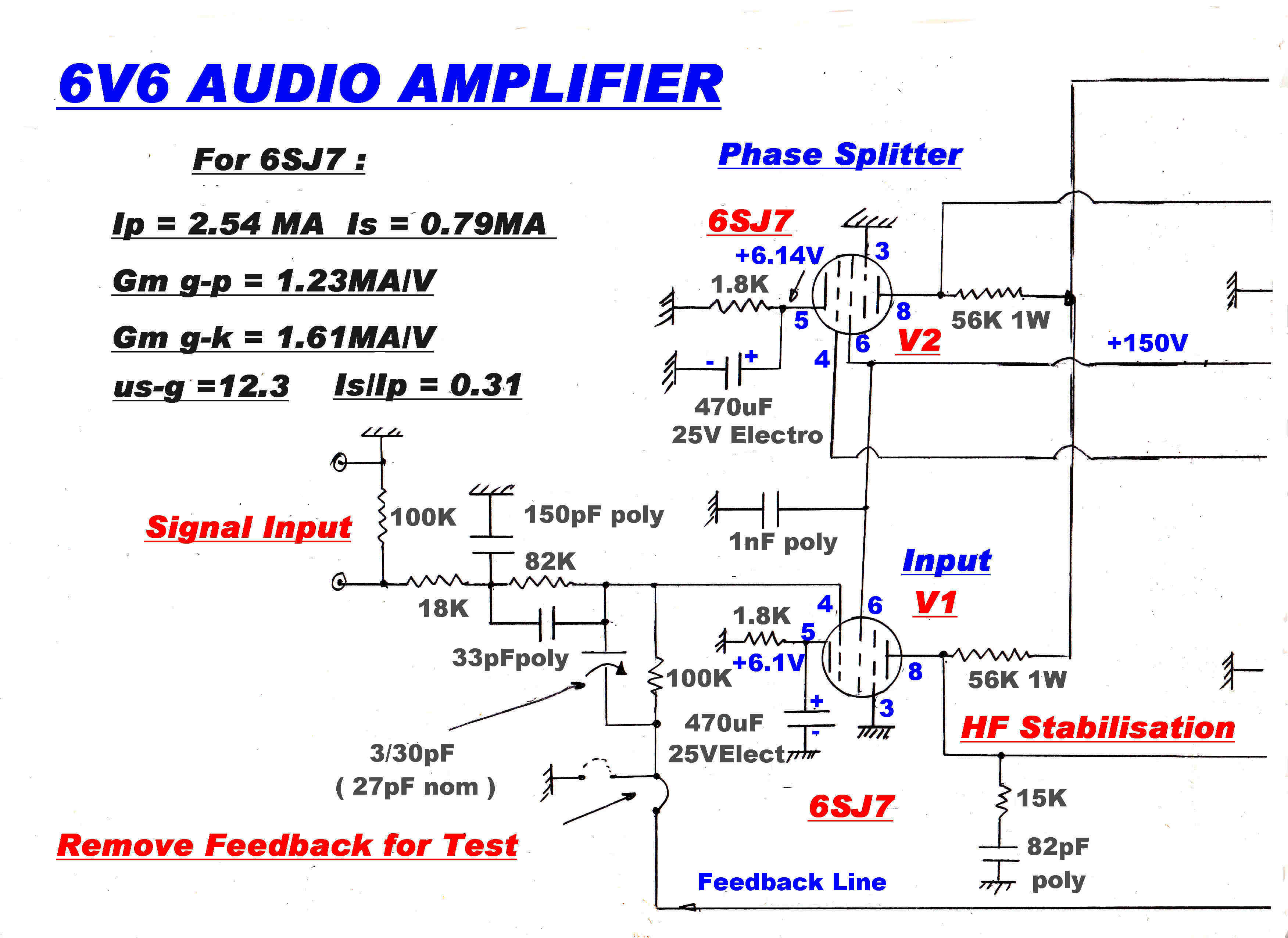
PHASE SPLITTER
The phase splitter is an operational amplifier V2 V3b [ 6SJ7 6SN7 ].
The gain depends on the ratio of passive elements [ 1Meg 27pF ] and so is very stable over time.
The low frequency balance in the push - pull amplifier is set by the ratio of the resistors marked 1Meg. :
the high frequency balance by the ratio of the capacitors marked 27pF.
The two adjustments do not interact and so are easy to set.
The total cathode current in the output stage is returned through a 1 ohm resistor to earth. [ not shown]
When the push - pull output stage is balanced, there is no signal across this resistor.
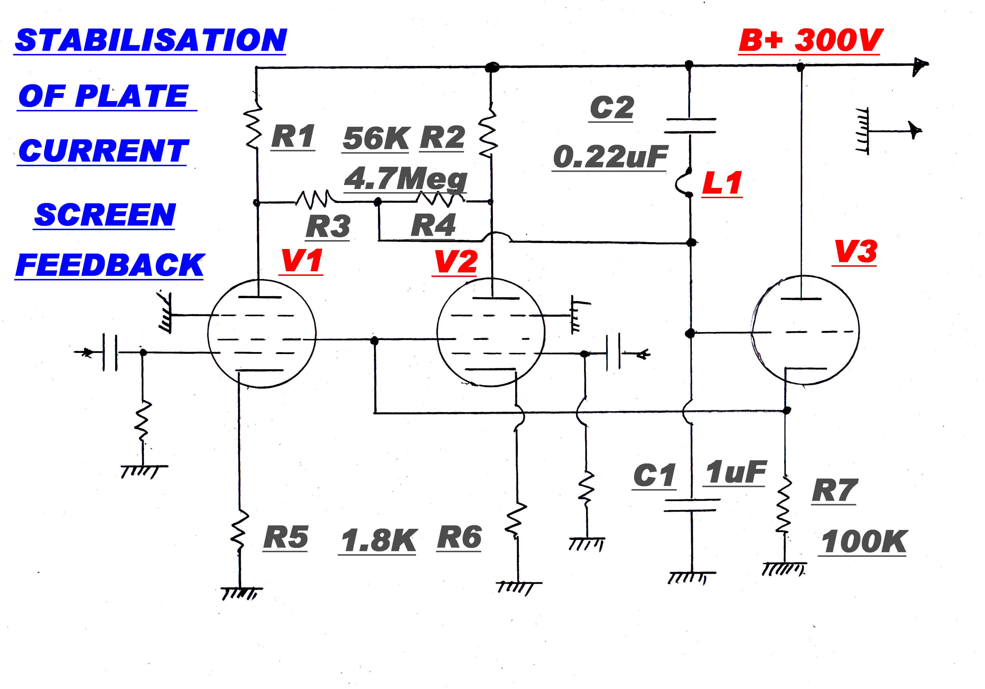 The ratio k ( = Is/Ip ) of screen current to plate current in small pentodes such as the 6SJ7 or 6AU6 depends
on the alignment betwen the turns of the grid and screen structures. Since this is random the ratio k can
vary over fairly wide limits.
The ratio k ( = Is/Ip ) of screen current to plate current in small pentodes such as the 6SJ7 or 6AU6 depends
on the alignment betwen the turns of the grid and screen structures. Since this is random the ratio k can
vary over fairly wide limits.
The screens are usually fed from a dropping resistor and bypassed to earth through a large capacitor to
remove any signal.
This technique has the following disadvantages:-
(1) The variation in k produces a large variation in screen voltage and so quiescent plate currents.
(2) The capacitive bypassing produces a fall in gain at some low frequency which can destabilise low
frequency feedback loops.
The circuit shown overcomes both disadvantages.
Initially, imagine the link L1 open.
(1a) R3 and R4 in parallel together with C1 form a low pass filter. The average plate voltage of the two pentodes
V1 and V2 is applied to the grid of the cathode follower V3 through this filter and then to the screens -
forming a feedback loop.
Since the cathode follower has a low output impedance, the spread in screen currents is of no consequence
and the important parameter - the plate voltage - is stabilised.
Any tube drift occurs only slowly , so the large time constant (2.35) seconds is more than adequate.
(2a) If V1 and V2 are opposing stages in a push - pull amplifier, then the signals on each
plate are equal and opposite, so no signal appears at the junction of R3 and R4. No signal is fed back to the screens and
the low frequency response is unaffected.
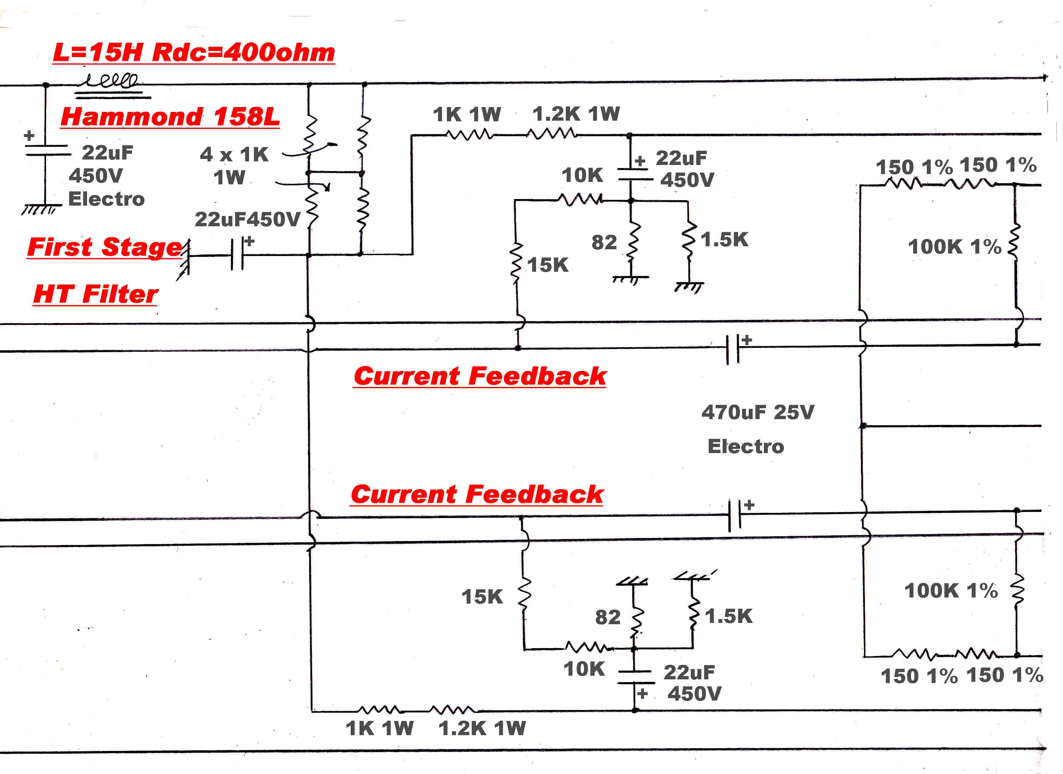
REJECTION OF RIPPLE ON THE HIGH TENSION LINE
Since the plate resistance of a pentode is very high, voltage variations on the high tension line can
appear directly on the pentode plate via R1 and R2.
If L1 is now closed, fast HT variations ( eg 100 Hz ripple ) will appear on the grid of the cathode follower via
the capacitive divider C1, C2.
A positive going signal on the HT line will appear on the screens and increase the plate current.
This produces a negative going signal which can cancel out the direct signal on the plate if the
capacitive divider is dimensioned correctly.
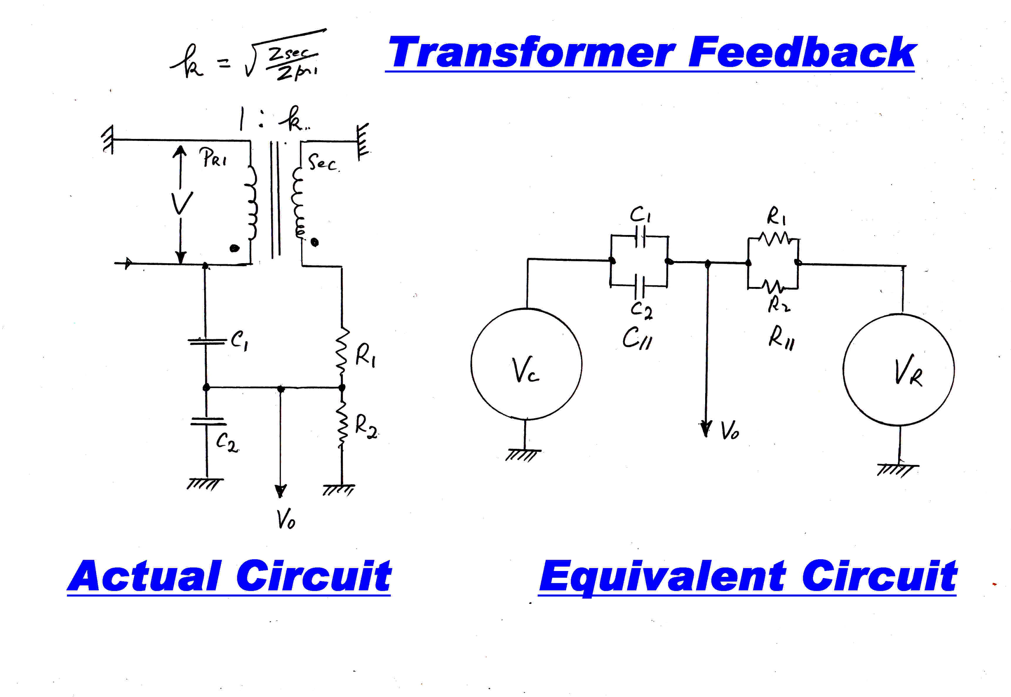
 The transfer function of the output transformer is usually the limiting factor on the
amount of feedback tolerated in the main overall loop.
The transfer function of the output transformer is usually the limiting factor on the
amount of feedback tolerated in the main overall loop.
The self capacity of the primary and the leakage reactance between primary and secondary form
two high frequency (destabilising) poles.
The feedback MUST come from the scondary( or load ) over the working frequency range of the amplifier.
This signal is affected by the full transfer function of the output transformer. For frequencies above this,
the signal can be drived from the transformer primary, since it is only required for feedback loop stability.
The network to perform this function is shown opposite.
It is discussed in more detail later.
DESIGN PHILOSOPHY
[A] OVERALL SPECIFICATION--- BANDWIDTH -- TRANSIENT RESPONSE
Virtually all audio signals applied to the input of the amplifier will have been bandwidth
limited by a low pass sharp cutoff filter. This applies to signals derived from CDs, FM and AM
Tuners and, to a lesser extent, from analog discs.
The cutoff frequency is usually well below 30KHz, so the guidelines adopted for the
design are:-
(1) Response: Flat and as near as phase linear as possible between 20Hz. and 30KHz.
(2) Non-linearity, that is intermodulation, as small as possible over this frequency range.
It is assumed that the detailed response outside this range, providing it is well behaved,
( ie no great peaks or troughs ) is of little consequence.
The response to a fast step function ( rise time < 0.1uS ) gives a complete picture of
amplitude and phase response.
A more realistic assesment of the dynamic response to a typical bandwidth limited audio signal
is given with a Si function input : generated by passing a step function through
a phase linear infinitely sharp cutoff filter.
Here the cutoff requency is fo = 30KHz so:
(ωo = 2 π 3x10⁴ rad/sec )
From the Fourier integral we have:-
vin(t) = 1/2 + (1/π) ∫o ωo
[(sin( ω t ))/ ω] dω
Or: vin(t) = 1/2 + (1/π) ∫o ωot
[(sin( ω t ))/ ω t] dωt
Or: vin(t) = 1/2 + (1/π)Si( ωot )
From Si function tables we see that it goes from 7% to 93% of full scale
in π/ωo = 0.5/fo
Here fo = 30KHz, so τ = 16.7uS
An amplifier with the above specification does not add anything or take anything away from
the signal. It just produces a bigger version of the input signal.
The statement that "valve amplifiers give a warm sound" is a complete mystery to me.
There are a large number of both valve and solid state amplifiers in the house. If I could
pick - aurally - which amplifier was in use, then I would consider that there was a fault
in the amplifier.
There are just good amplifiers - solid state or vacuum tube. They have no "sound".
[B] LONG TERM STABILITY --- LINEARITY
Stability and linearity are obtained by degeneration and the use of internal feedback loops.
The operating point, or quiescent current, in each tube is stabilised with the use of individual
cathode bias resistors.
The average DC plate voltages of push pull voltage amplifier stages is filtered and fed back
to the screens to further stabilise the operating point.
This stabilises the average value. It does not cover drift between the two tubes
in opposite directions.
The screen feedback does not modify the low frequency response for push-pull signals.
Gain stability and linearity are enhanced by the use of internal feedback loops.
Internal feedback loops have the following advantages:-
(1) The transfer function of internal loops is usually little affected by external loads.
(2) The transfer function can be chosen to tolerate a high degree of feedback.
For instance, the feedback may be over just two stages. This will usually provide a
favourable open loop response for feedback.
The closed loop response of the internal loops can also be tailored to give stability in
the overall feedback loop.
The ultimate aim is to make the gain virtually dependent only on the ratio of two resistors.
This is possible when the limit on the gain bandwidth product of the tubes is not approached -
a condition usually met in audio equipment.
[C] USE of PENTODES in OUTPUT STAGE
The over-riding consideration in the output stage is power output and efficiency.
The plate of a pentode can swing to a much lower voltage than a triode giving greater efficiency
and power output.
A pentode has a very high plate resistance and, so without corrective measures, produces
an amplifier with a high output impedance and added distortion at low frequencies due to
magnetising current distortion in the output transformer.
It is shown below that overall voltage feedback from the secondary of the transformer
will reduce both of the above effects to any desired level.
The reduction of distortion with a triode working into a transformer primary (with
resistance) is limited.
The resistive output impedance of the amplifier adds to the resistance of the speaker
voice coil and speaker leads. This determines damping at low frequencies.
The DC resistance of the voice coil of a nominal 4 ohm speaker can be between 3 and 3.5 ohm,
so an output impedance of, say, less than 1 ohm, has little effect.
Negative voltage feedback coupled with positive current feedback can produce a
negative output resistance from an amplifier to cancel some of the positive resistance
of the voice coil.
The next step up from this is to produce a bridge on the output to reveal the motional
voltage produced by the speaker. This can be used as the feedback signal.
This modifies the dynamics and covers distortion due to non-linearities in the
elastic suspension of the cone. It does not cover distortion due to non-uniform
magnetic fields.
All variables are covered by motional feedback from the cone: valid
for frequencies before cone break up.
[D] CURRENT FEEDBACK on OUTPUT STAGE
Much of the distortion in a tube audio amplifier comes from the non-linear relationship
between the plate current and grid voltage in the output stage.
This can be reduced by local feedback.
Local voltage feedback over the push-pull output stage is sometimes taken from either side of
the primary of the output transformer.
It is shown below that this results in an output stage very sensitive to unbalanced
drive and component drft - just the effects feedback is supposed to cure.
Analysis shows that the trouble is caused by the common coupling between both sides
of the push-pull output stages through the transformer primary.
A feedback loop on one side should not be influenced by the signal on the other side.
This means that the output stage plate voltage should not be used for feedback.
The cathode current in the output tubes is independent and should be used.
The output signal of interest is the plate current NOT the cathode current.
In a triode there is no problem in taking this feedback from a cathode resistor since,
for audio frequencies, the cathode current equals the plate current.
The pentode creates greater difficulties.
As the plate voltage falls to low values, a virtual cathode is formed between
plate and screen and the fraction of the cathode current intercepted by the screen rises.
To get true plate current feedback, the screen current must be subtracted from
the cathode current and this used as the feedback.
The most simple way to do this is to feed each output screen through
a resistor and bypass the screen directly to the cathode. Changes in cathode
current are then identical with plate current changes for all frequencies where the bypass
capacitor is active.
The screen resistors also provide DC feedback and stabilise the quiecent current of the tube.
This amplifier would require eight large electrolytic bypass capacitors, so a compromise was made
to use only two.
The four screens on either side were tied together.
This stabilises the total plate current, but not the plate current of each individual tube.
In this amplifier individual unbypassed cathode resistors provide current sensing and
degeneration on each output tube. The degeneration stabilizes and linearises the tube
transfer characteristic and reduces the upward drift of DC input current with drive.
When all four networks are considered in parallel, the total cathode current is effectively
sensed by a 75 ohm shunt with an output resistor of 25Kohm.
The effective shunt resistor in the screen is 75 ohms and a 25 Kohm output resistor is
added to make it identical to the cathode sensing network. The voltage at the junction of
these two 25K output resistors gives a true measure of the total signal plate current on one
side of the push-pull output stage.
The difference between the demand and the actual output current is generated in the
470K feedback network, and the error applied to the grid of the 6AC7 pentode output drive
amplifier.
Because of the high loop gain, this current feed back system produces an output stage
with extremely low distortion and very low drift in characteristics, since its performance is
determined largely by the ratio of resistors.
[E] OUTPUT STAGE COUPLING NETWORK
The grid of each output pentode has its own R-C coupling network. This aids service and
prevents grid current in any one tube from interfering with the bias on other tubes.
The dominant high frequency stabilizing pole in the loop is formed by the resistive
load on the 6AC7 driver and the input capacity of the output tubes. Because of the
screening action within the tetrode 6V6s, the stability of this loop is virtually independent of
the output load.
If the instantaneous gain of a system under feedback goes to zero, very large
driving errors can build up in the loop.
In AC coupled vacuum tube systems this tends to drive the grid positive through
a coupling capacitor. Grid currents can result in a large charge accumulating
on the capacitor. This can paralyse the amplifier and take considerable time to leak away.
An AC coupled output stage with internal feedback is subject to overload paralysis.
Here 220K resistors are added in series with the grids of the 6V6 output tubes to
limit the grid current on overload. 150pf capacitors in parallel prevent them from changing
the high frequency transfer function, and so the stability.
The amplifier has a fast recovery from heavy overloads.
AM transmitters with heavy envelope feedback are prone to the same trouble when the carrier
goes to zero.
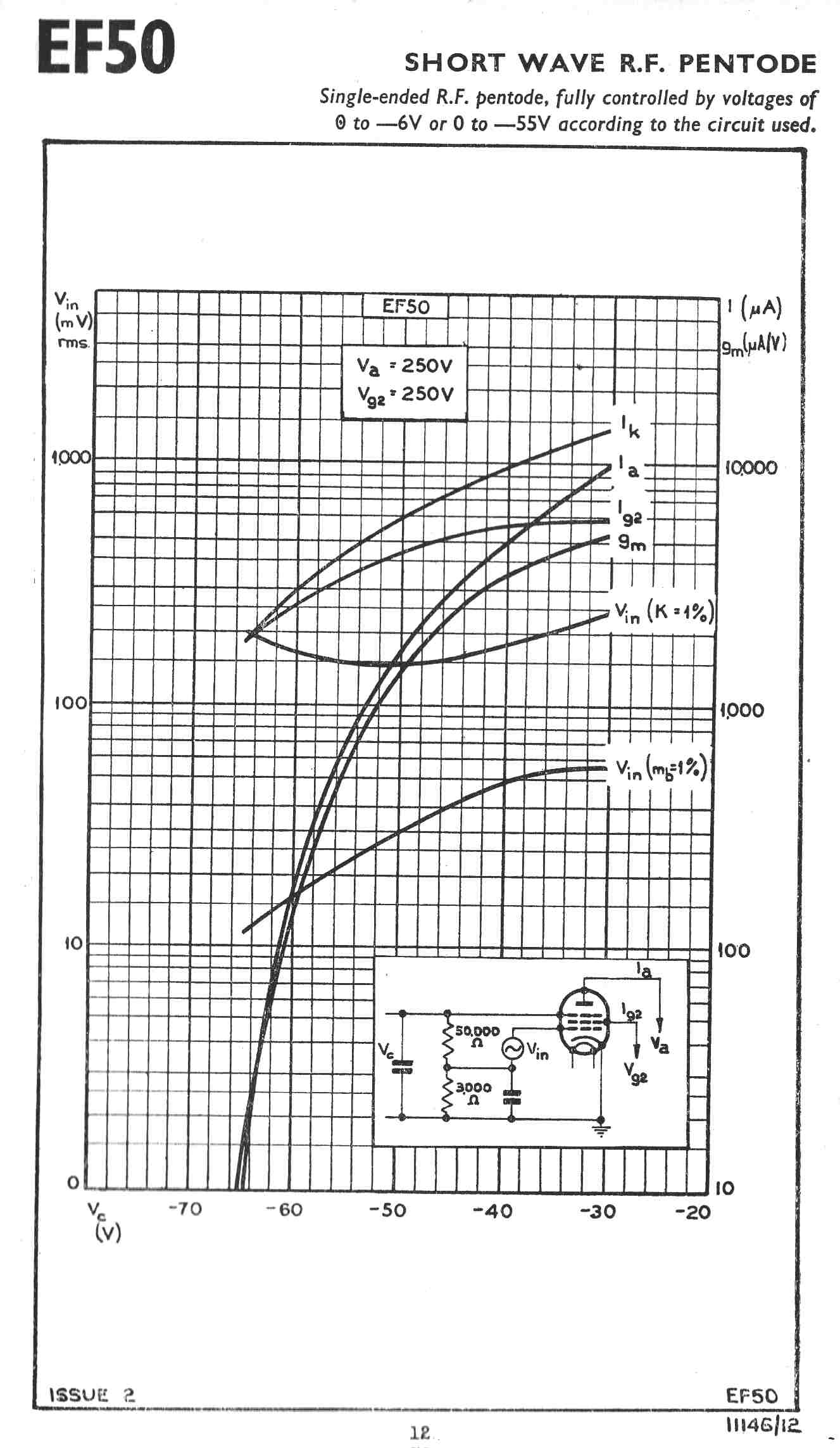
In 1938 the 6AC7 had the highest gain bandwidth product of any regular tube on the market.
It was designed for TV IF strips. It was chosen here to give maximum gain around the
output stage feedback loop.
Millions were produced during WWII for the wideband IF strips of PPI radar.
The equivalent tube used by the British and designed by Philips was the EF50.
The equivalent tube in German equipment was the EF14.
The 6AC7 and the EF14 were metal tubes.
It would appear that only the US and the Germans knew how to manufacture metal tubes.
[F] THE PHASE SPLITTER
The 6SJ7/6SN7 phase splitter is really an operational amplifier with a loop gain of 33.
The front and feedback networks are a 1Meg resistor paralled by a 22pF capacitor.
The R and C of the feedback network are made adjustable to alter the balance of the drive to
the output stages.
The balance therefore depends on the ratio of two resistors and is very stable.
[G] OVERALL FEEDBACK
The overall feedback loop is used to reduce the output impedance to a low value and further reduce
the distortion, especially at low frequencies due to the non-linear magnetization current required by
the output transformer.
In all amplifiers the primary winding resistance of the transformer and the output resistance
of the output tubes produce distortion in the secondary voltage at low frequencies because of
non-sinusoidal magnetizing currents. Here the situation is a bit worse than with triodes or
ultra-linear pentodes because of the high output impedance.
More feedback must be used in the overall loop to cover this.
The high frequency transfer function of the output transformer usually limits the amount of feedback
which can be safely applied.
Here a technique is used to greatly improve loop stability.
A capacitive voltage divider from the primary of the transformer is paralleled with a resistive
divider from the secondary. The division ratio is chosen so that, if the transformer is ideal,
the output from the two dividers in equal.
For frequencies up to about a hundred kilohertz, the output comes from the transformer secondary:
above this from the transformer primary: thus bypassing the extra phase change due to the self
capacity of the high impedance primary, the leakage reactance of the transformer and the
impedance of an indeterminate load.
[G] ASYMMETRIC DRIVE
In almost all class A push-pull amplifiers the drive on the grids of the output tubes produced
by the phase splitter is symmetrical -
the drive on one grid is the negative of the drive on the other grid.
The peak positive drive is equal to the peak negative drive.
The transfer characteristic ( Ip/Vg) of the output pentodes (6L6/6V6) is a square law.
They require a much greater negative voltage swing on the grid to turn off than on the positive cycle
which drives the grid to zero volts.
The result is that the output tubes are never cutoff with a consequent waste of power.
The high degree of feedback in the current loop produces an asymmetric voltage drive to
the grids of the output tubes.
This ensures that the output tubes cutoff at full power output.
|
|
|
6L6 PLATE CHARACTERISTICS |
6L6 TRANSFER CHARACTERISTIC |
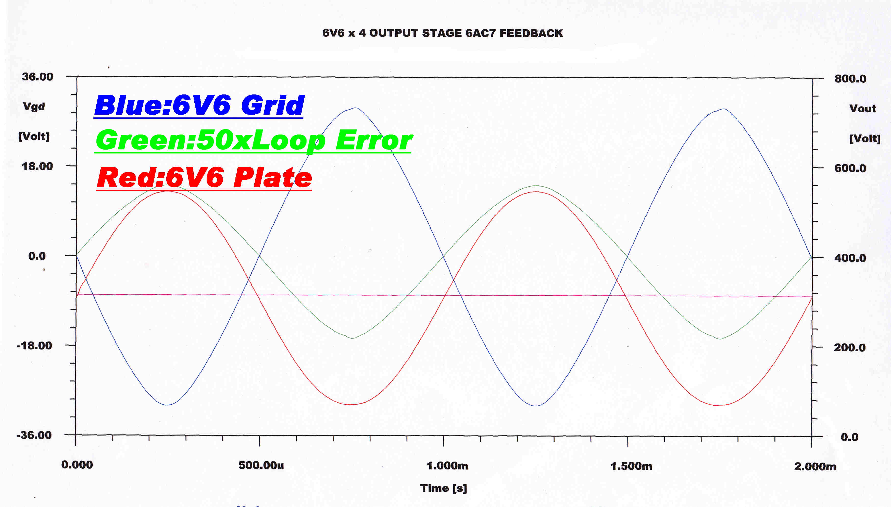
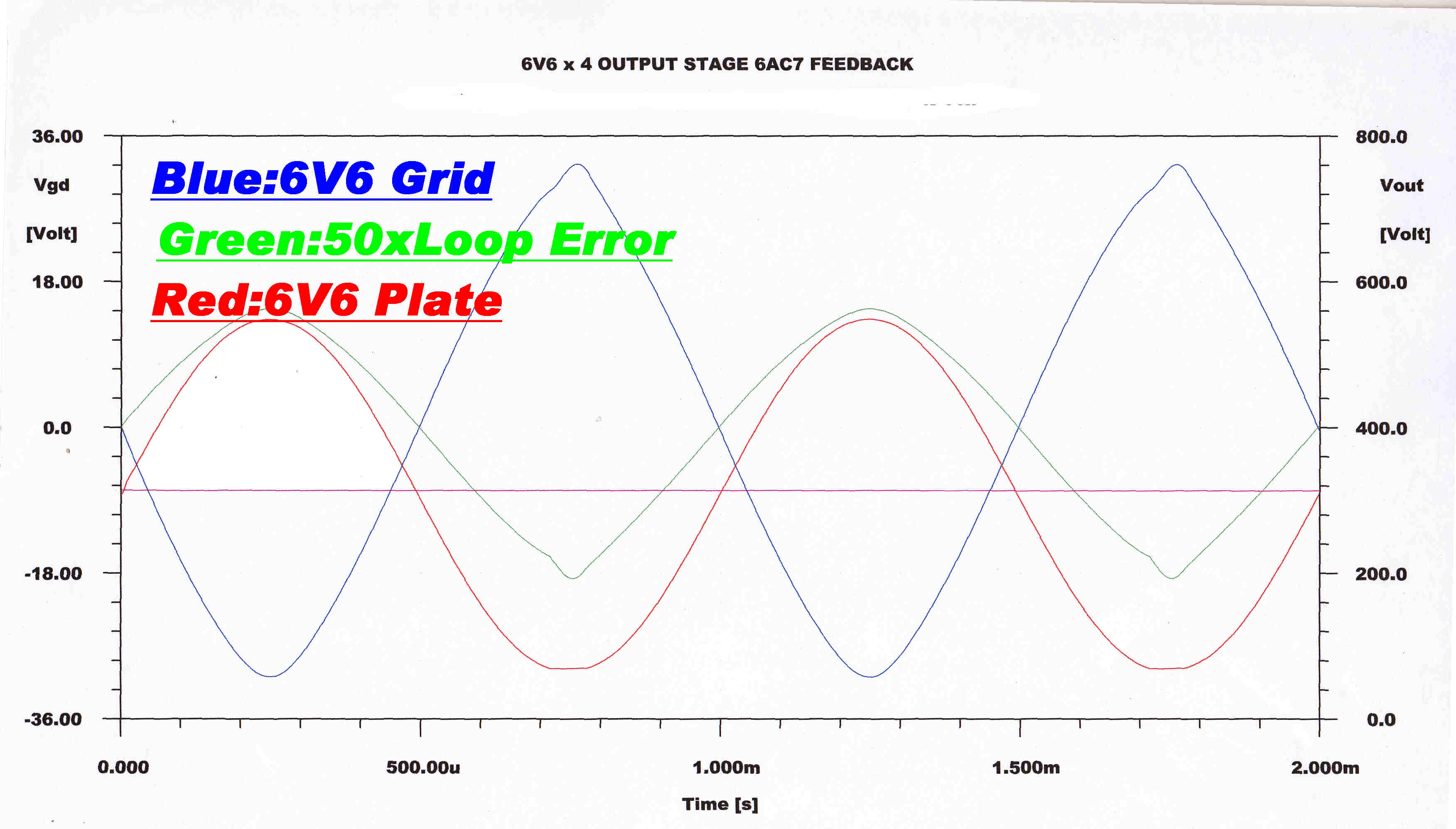
The large gain around the current feedback loop produces an asymmetric drive on the grids of the
6L6 output tubes.This contains a DC component.
For short transients the operating conditions on the driver do not change. If the amplifier is forced to produce full output
for a prolonged period, the operating conditions on the driver (DC plate current - grid bias) change. This is accompanied by
a slow speed transient in the current feedback loop.
This is characteristic of all AC coupled systems with non-linear elements.
The plate (output) voltage, the grid drive and the current loop error are shown below
for the following conditions:
[A] Just before full power output
[B] At full power output
[C] Just after overload
|
|
|
|
Just before full power |
At full power |
Just after overload |
The unbypassed cathode resistors in the output stage stabilise the quiescent plate current and
linearise the transfer characteristic.
The magnitude of DC transients in the current feedback loop is reduced.
The output tube with the cathode resistor can be regarded as a tube with linearised characteristics.
The plate characteristics for such a tube together with those for the raw tube are shown below.
|
|
|
BEAM TETRODE PLATE CHARACTERISTIC |
PLATE CHARACTERISTIC WITH UNBPASSED CATHODE |
FULL CIRCUIT DIAGRAM
The full circuit diagram of the amplifier is shown below.
It is a slightly modified version of an amplifier which has been in operation for
about twelve years.
The low frequency compensation in this amplifier has been redesigned to give a better
phase margin.
It must be stressed that this version of the low frequency compensation is yet
to undergo testing.
Note: See below for a larger version of the circuit.
|
|
|
|

|
|
|
|
|
TRANSFORMER MAGNETISING CURRENT : DISTORTION AT LOW FREQUENCIES
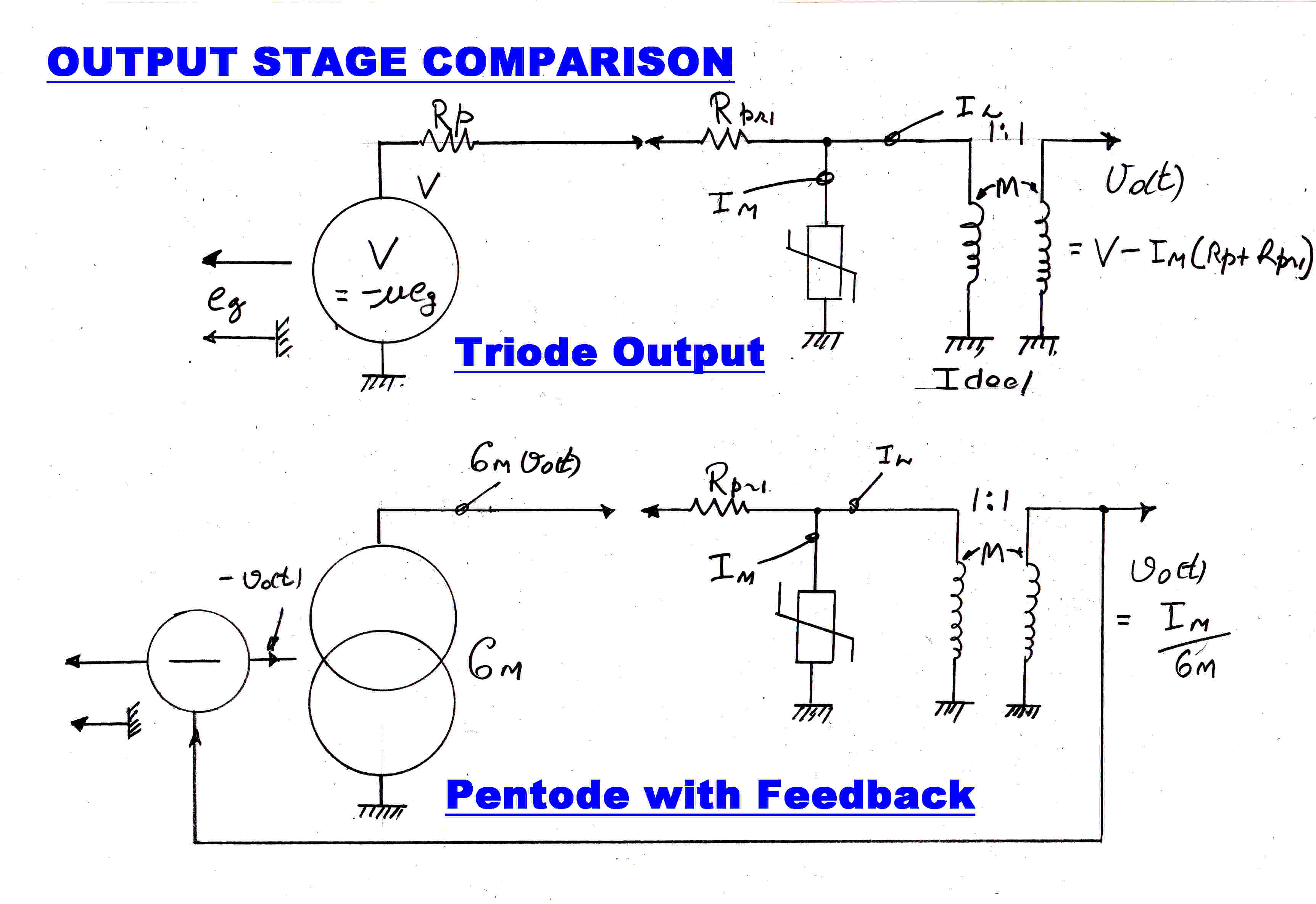 The equivalent circuit of a triode output stage and pentode output stage with feedback
is shown opposite.
The equivalent circuit of a triode output stage and pentode output stage with feedback
is shown opposite.
The output transformer is represented as an ideal transformer with a non-linear
impedance shunting the primary. The non-linear impedance generates the magnetising current.
Let us calculate the distorted output voltage vo(t).
For the triode:-
vo(t) = Im[ Rpri + Rp ]
For the pentode we have:-
Im = Gmvo(t)
ie vo(t) = Im/Gm
Even for triodes with very low plate resistance we have an irreducible minimum of:-
vo(t) = ImRpri
For a pentode with feedback, vo(t) can be made as small as we like by
increasing the loop gain Gm.
Note:- The feedback must be taken from a winding other than the primary.
We can now sum up:-
The output stage must be made to "cough up" the magnetising current, so distorted voltge
must appear on one of the tube's electrodes in order to produce this current.
In the case of a triode without feedback, distorted voltage appears on the plate and
also in the output.
In the case of a pentode with feedback, the distorted voltage appears on the grid, and so
the distortion in the output may be reduced by any amount by increasing the feedback.
This, of course, also lowers the output impedance at the same time.
SYMMETRICAL FEEDBACK LOOPS FROM OUTPUT TRANSFORMER
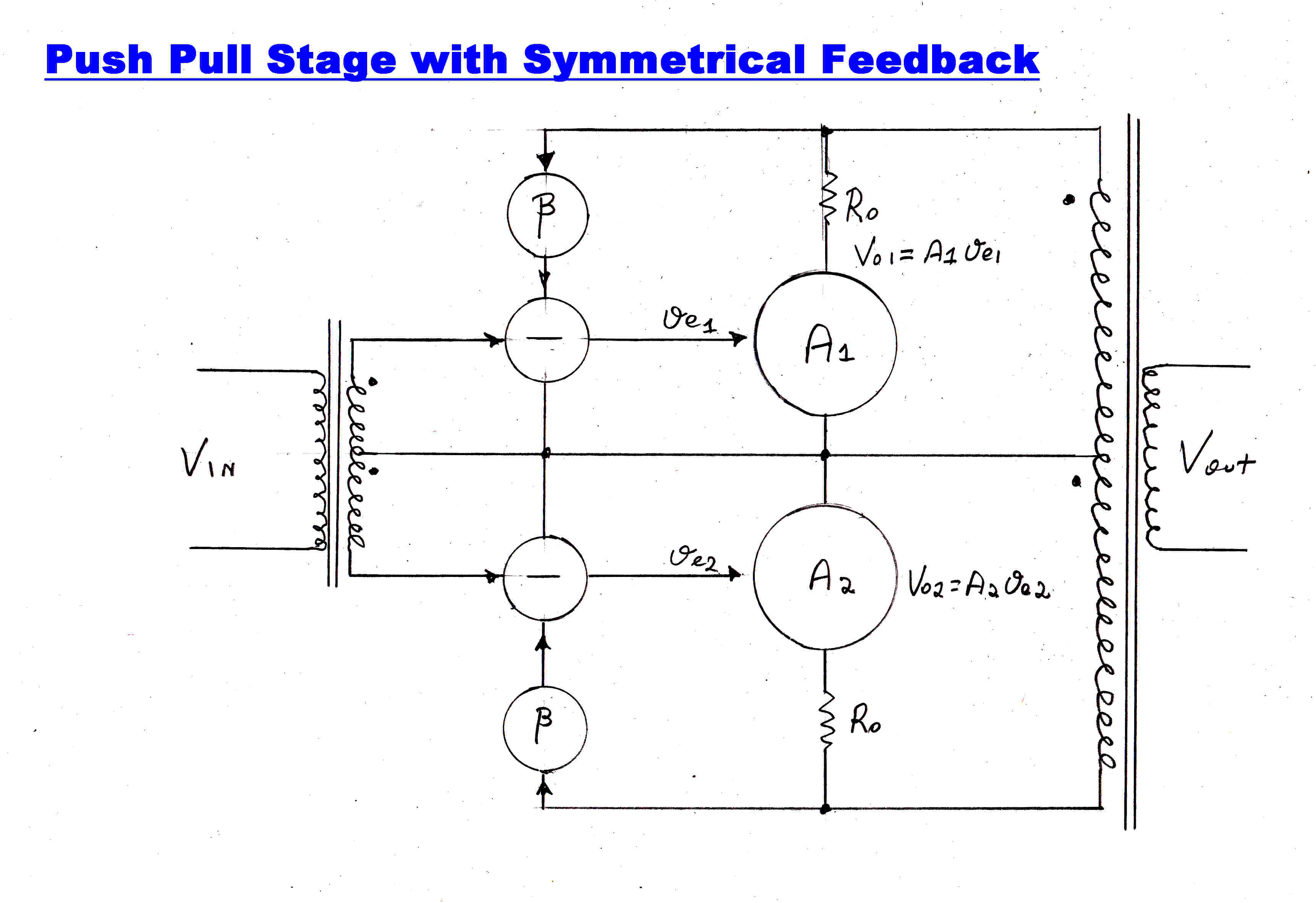 The block diagram of a push pull output stage with symmetrical feedback loops
is shown opposite.
The block diagram of a push pull output stage with symmetrical feedback loops
is shown opposite.
It has been found that this topology gives rise to amplifers in which the output
stage balance is very sensitive to the drive balance.
It is also sensitive to component drift within the loop: a parameter which negative feedback
should be reducing - not increasing.
We now investigate the reason.
If we tease the circuit apart, it will be seen to be two feedback amplifiers sharing
a common load: in other words two feedback amplifiers in parallel.
Now the feedback reduces the output impedance of both amplifiers, so in reality, we have
two low impedance generators in parallel: a classical combination for poor load sharing.
The load on each amplifier is a parallel combination of the load Rl and the output impedance
of the other amplifier, which can be quite low because of the feedback. The gain of each
side for unbalanced inputs is therefore much lower than the common mode gain: the loop error
and hence the unbalance will be greater.
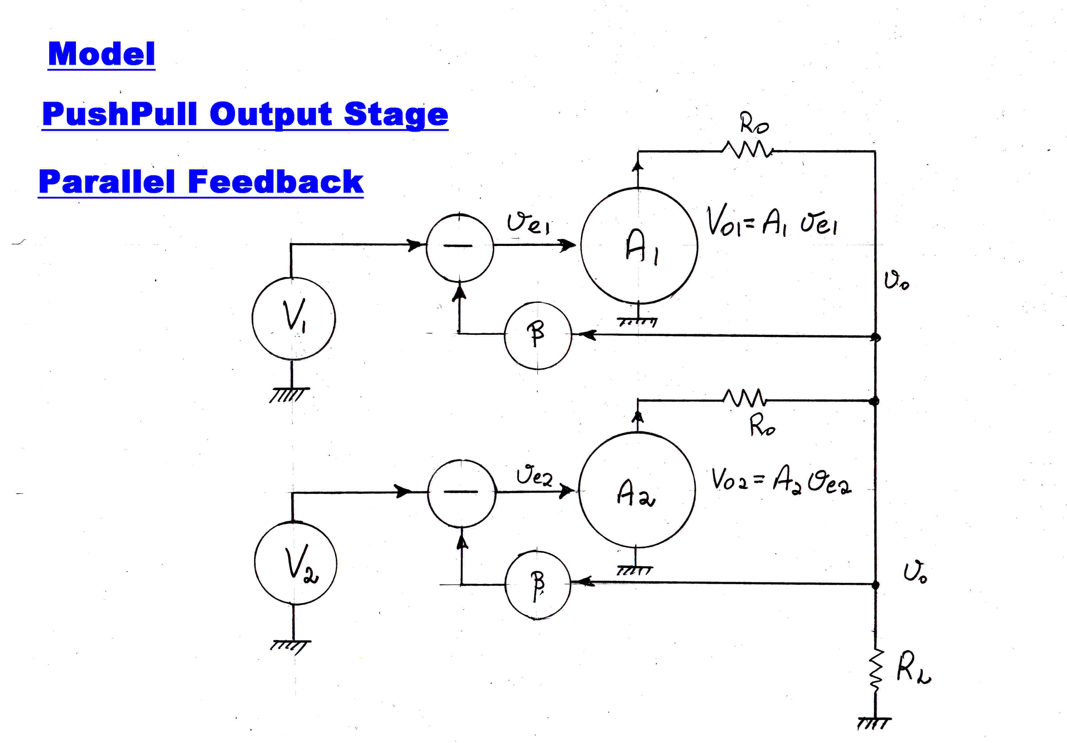 We now analyse the error signals in a push-pull stage with symmetrical feedback
from either side of the output transformer.
We now analyse the error signals in a push-pull stage with symmetrical feedback
from either side of the output transformer.
To simplify the algebra, and to emphasise the fact that two feedback amplifiers
are in parallel and sharing a common load, we redraw the amplifier as shown.
The push-pull amplifier now reduces to two feedback amplifiers in parallel.
The inputs are now in phase not push-pull.
&nbs; If we apply Thevenin to the output stage, each output generator has an equivalent voltage of
V/2 with an putput resistance of Ro/2.
This gives rise to the following identities:-
γ = vo/Vo1 = vo/Vo2
= 1/( 2 + Ro/RL )
We can then write:-
ve1 = V1 - βvo -----------(A)
ve2 = V2 - βvo -----------(B)
vo = γ( Vo1 + Vo2)-------(C)
= γ( A1ve1 + A2ve2)----(D)
ve1 = V1 - βγ( A1ve1
+ A2ve2 ) ------(E)
= V1 - βγA1ve1 - βγA2ve2
------(F)
ve1 + βγA1ve1 =
V1 - βγA2v
From (A) and (B) we get:-
ve1 - V1 = ve2 - V2 ----(H)
ve2 = ve1 - V1 + V2 ----(J)
Substituting (J) in (G) :-
ve1 = [ V1 + βγA2( V1 - V2 ) ]/
[ 1 + βγ( A1 + A2 ) ] -----(H)
Now let us consider what happens when an out of balance push pull drive
is applied to the system.
We can do this by putting V2 to 0 and perturbing
V1 by ΔV1
Suppose each side is balanced, so that A1 = A2 = A
Then, substituting in H, we get:-
Δve1 = ΔV1( 1 + βγA )/( 1 + 2βγA ) --------(J)
[The error on side 1 for an increase in drive on side 1 by ΔV1 ]
The error on side 2:-
We can calculate the error on side 2 (Δve2) by imagining a change in V2 and calculating
Δve1 . This is true because the system is symmetrical and linear.
We have:-
Δve2 = -ΔV1( βγA )/( 1 + 2βγA ) --------(K)
The error on side 2 for ΔV1 on side 1.
For a balanced drive:-
ΔV1 = ΔV2
Again, substituting in H, we have :-
Δve = ΔV1/(1 + 2βγA )----------(L)
The error in each channel for a balanced drive.
We now divide to find the ratio, R, of the errors on each side with an unbalance drive and
a balanced drive:-
R1 = 1 + βγA
R2 = - βγA
R1 is the return difference or the reduction of gain by the symmetrical feedback loops.
|R2| is the loop gain.
If the feedback is large, then a small amount of
unbalance in the push-pull input will cause a much bigger unbalance in the error signal,
and so the drive to the output stages - highly undesirable.
For instance, a 2% unbalanced drive will cause 20% unbalance with 20db of feedback.
This reduces the power output and increases the distortion.
The balance adjustment is much more sensitive and difficult to adjust.
Lesson: If feedback is to be applied over the output stage ( and driver ), then,
it should be taken from a point NOT influenced by the other side in a push pull amplifier:
for instance, the cathode of the output stage.
We can solve for the overall performance.
vo = γ [ A1V1 + A2V2]/
[ 1 + βγ( A1 + A2 )]
Large unbalanced signals cancel in the output transformer. In a linear system this is of no consequence,
but in a system with non-linrarities and limited dynamic "room" highly undesirable.
Since design is an intuitive process, it seems prudent to cover the above algebraic
explanation with a more heuristic approach.
When driven by identical signals (balanced push-pull inputs in real life) all points
in the two amplifiers are at the same potential - correcting for the 180 degree
phase change between sides.
They may be joined.
The system then degenerates into a single amplifier with half the output resistance.
To simulate an unbalanced drive, earth the input of one amplifier and apply the unbalanced
drive to the input of the other. This driven amplifier then works into a load comprising
the actual load in parallel with the output impedance of the other amplifier.
Because of the feedback this is low, so the gain of the signal amplifier is low.
Because of the low gain, the error signal will be much larger.
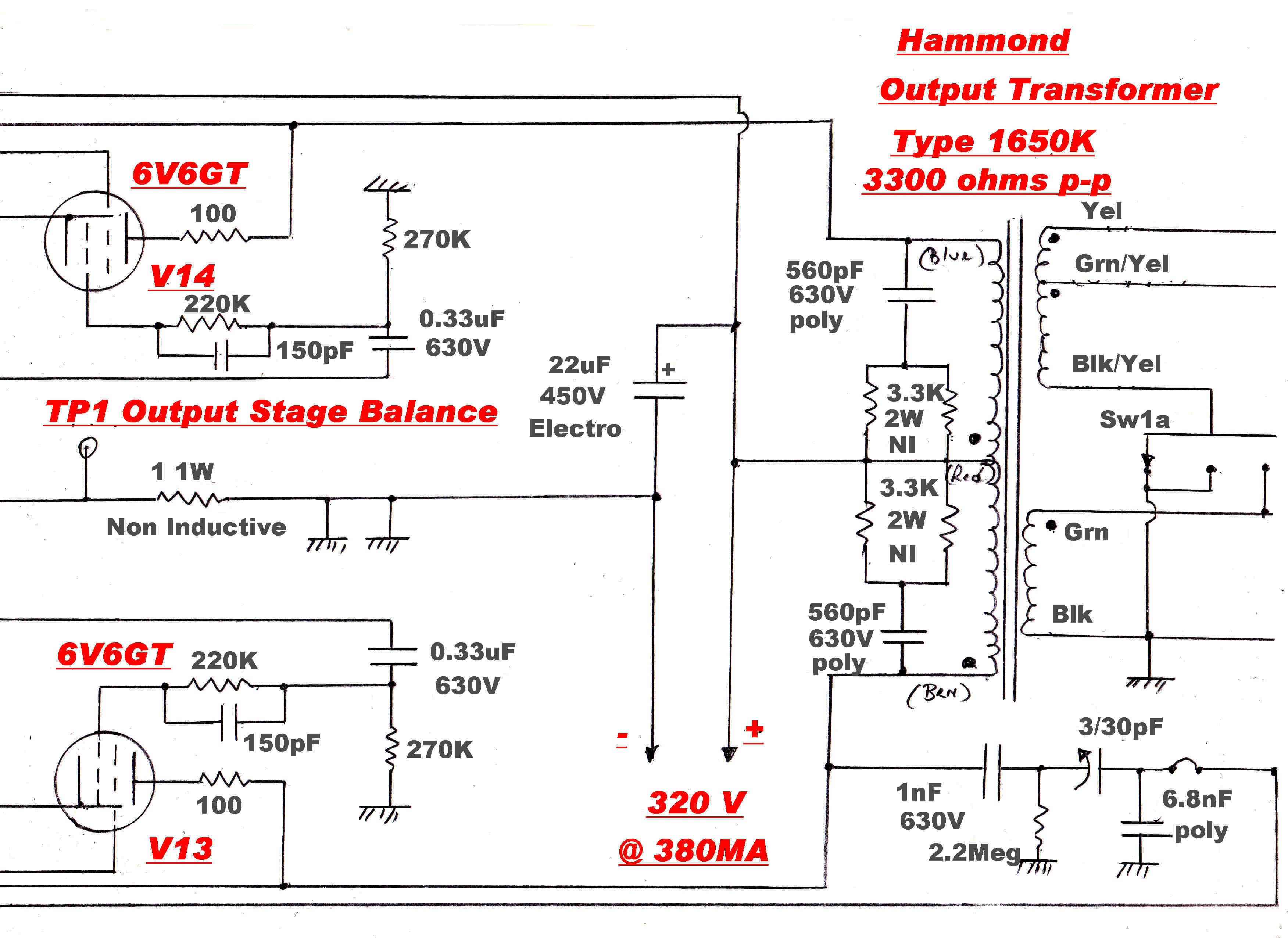
Symmetrical feedback over push pull output stages takes many forms.
In one the primary of the output transformer is split between cathode and plate.
This makes the output stage balance sensitive to the drive balance as indicated above.
Further, it increases the driver output voltage, and so its distortion.
One resistive feedback loop applied to the input is a better solution at
reducing distortion and output impdedance.
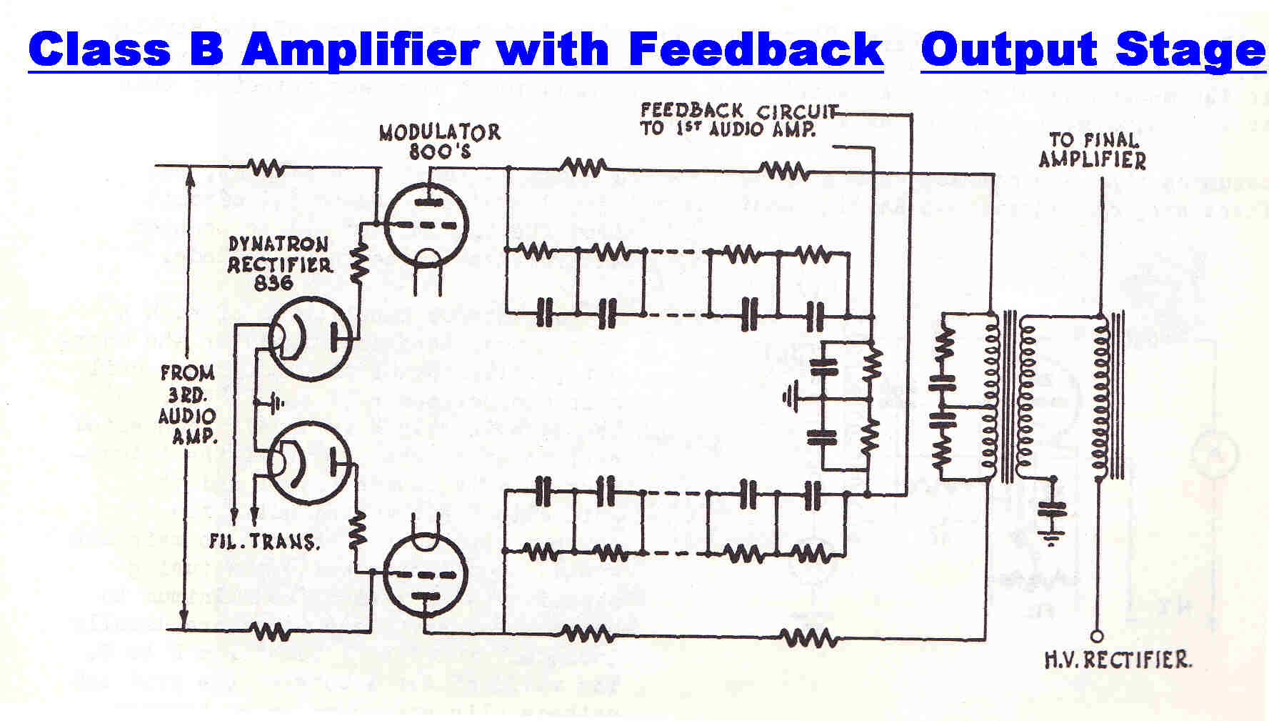
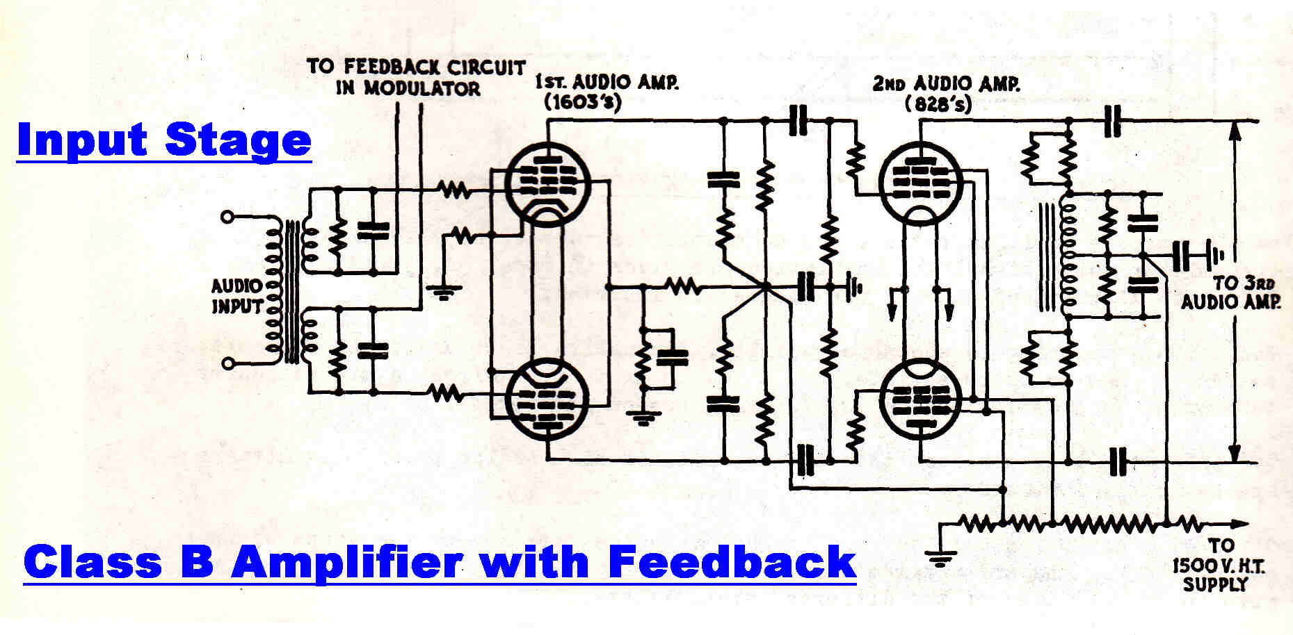 The circuit of a class B high power audio amplifier used for high level plate
modulation in an AM transmitter is shown on the right.
The circuit of a class B high power audio amplifier used for high level plate
modulation in an AM transmitter is shown on the right.
It is taken from a PMG training manual and is typical of the type used in most high level
modulated transmitters.
It is noted that the symmetrical feedback loops cover all amplifier stages and would therefore
seem to violate the principle described above.
This is not so, for only one side of the output stage is active at one time except for a small
crossover region.
The amplifier really consists of two independent amplifiers: one for the positive cycle and one
for the negative cycle.
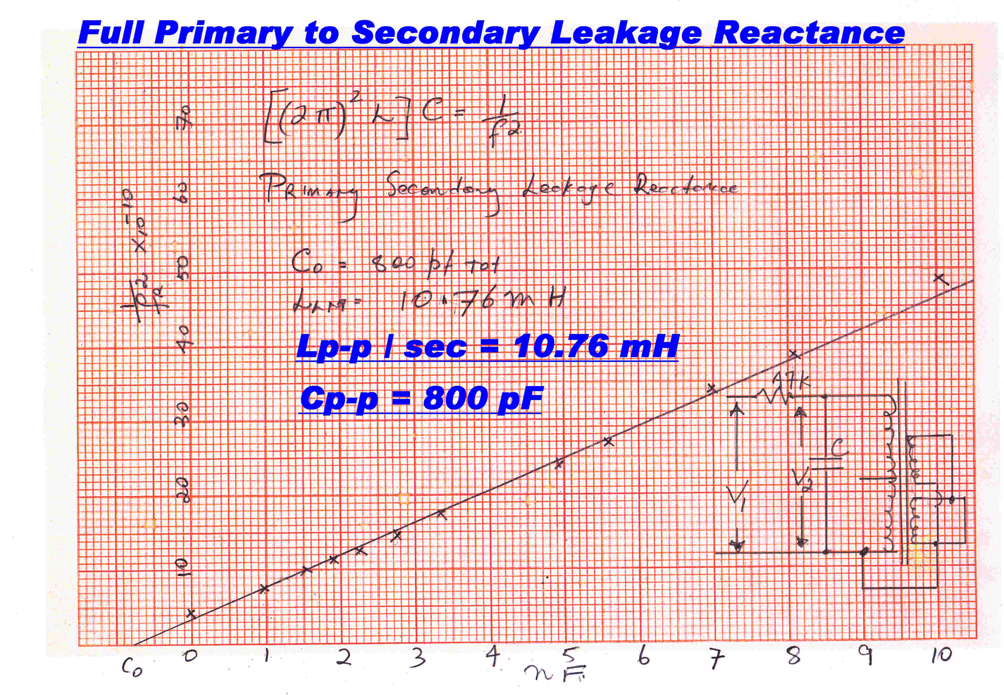
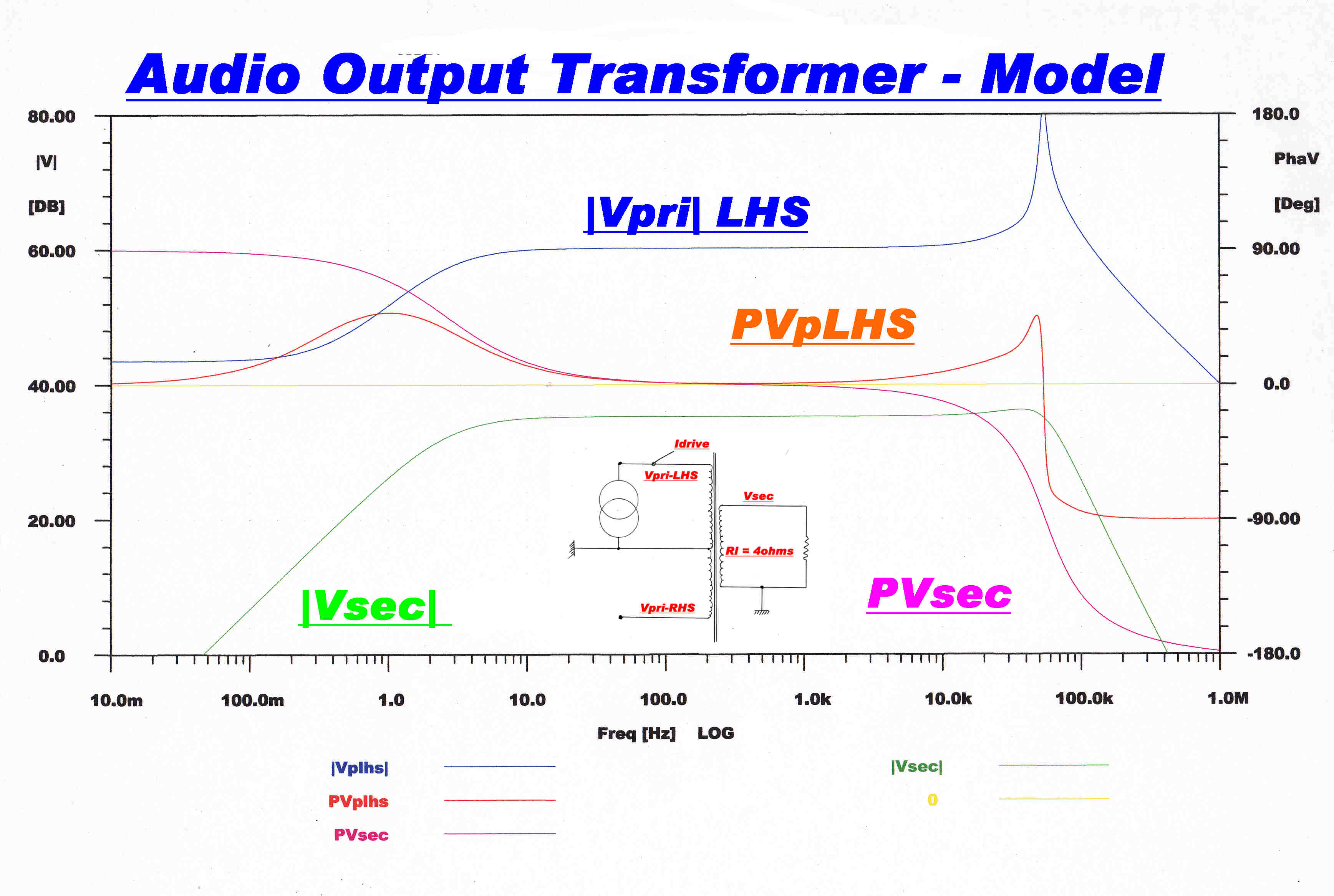
OUTPUT TRANSFORMER MODEL
High Frequency Measurements: Leakage Inductance : Winding Capacity
The winding capacity in transformers is distributed, and so can only be roughly approximated by models with a finite number of lumped components.
The classical method of measuring the leakage reactance and self capacity of a winding
is as follows:-
(a) Short the other winding.
(b) Shunt the winding with capacitors of known value and note the parallel
resonant frequency .
(c) Plot the variable 1/(fr)2 against C.
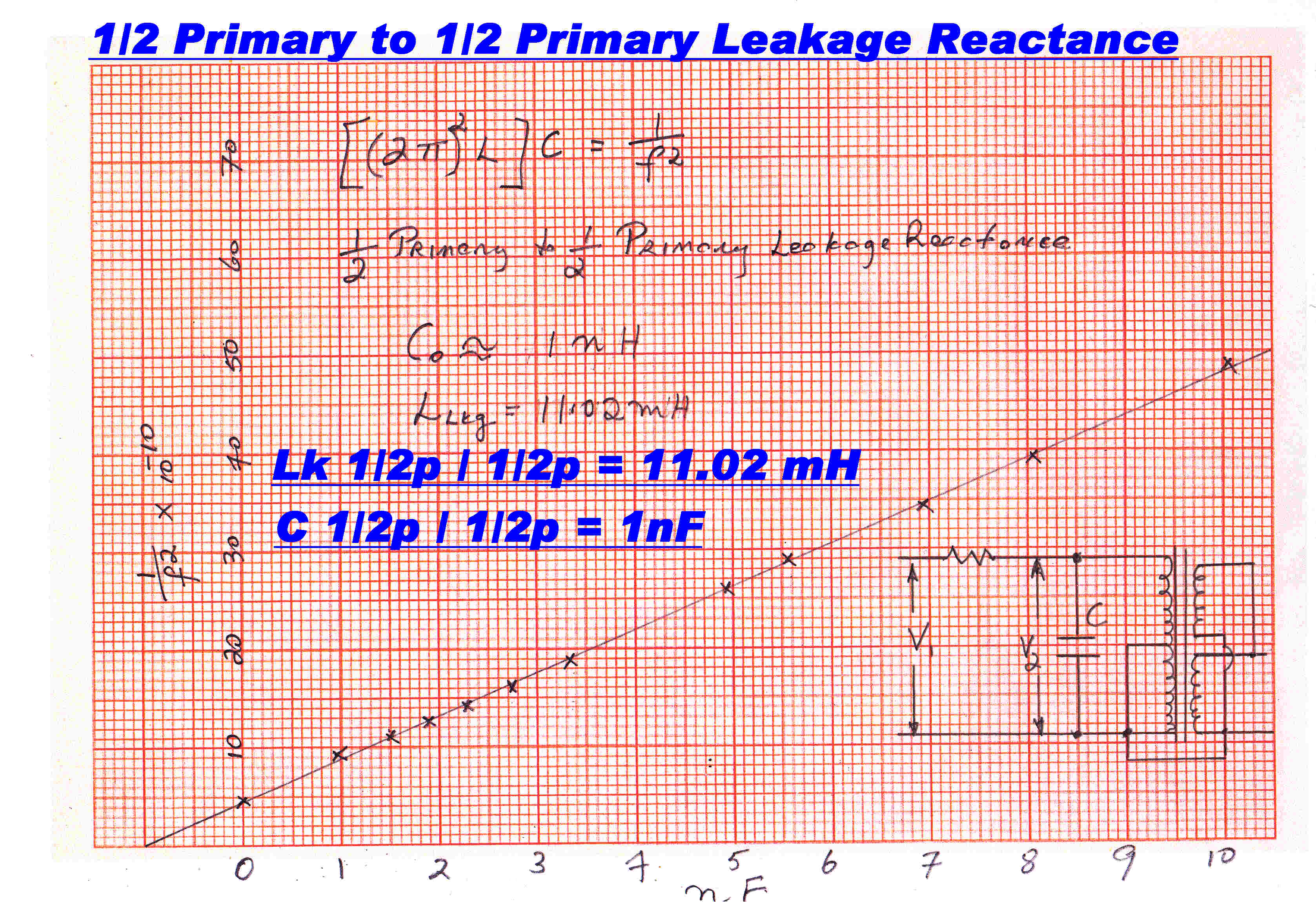
Plots to find the self capacity and leakage reactance between:-
(a) The total primary and secondary of an output transformer
(b) The two halves of the primary of a push-pull transformer.
|
|
|
From the slope of the curve the leakage inductance is seen to be 10.76mH. |
Here the secondary is left open and one side of the push-pull primary
is shorted. |
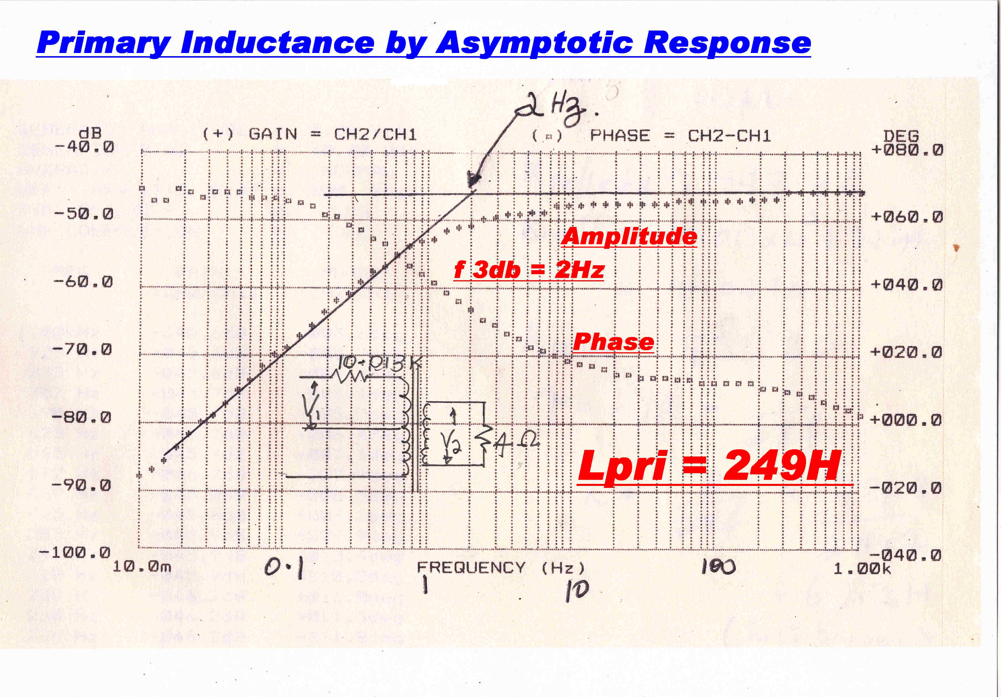
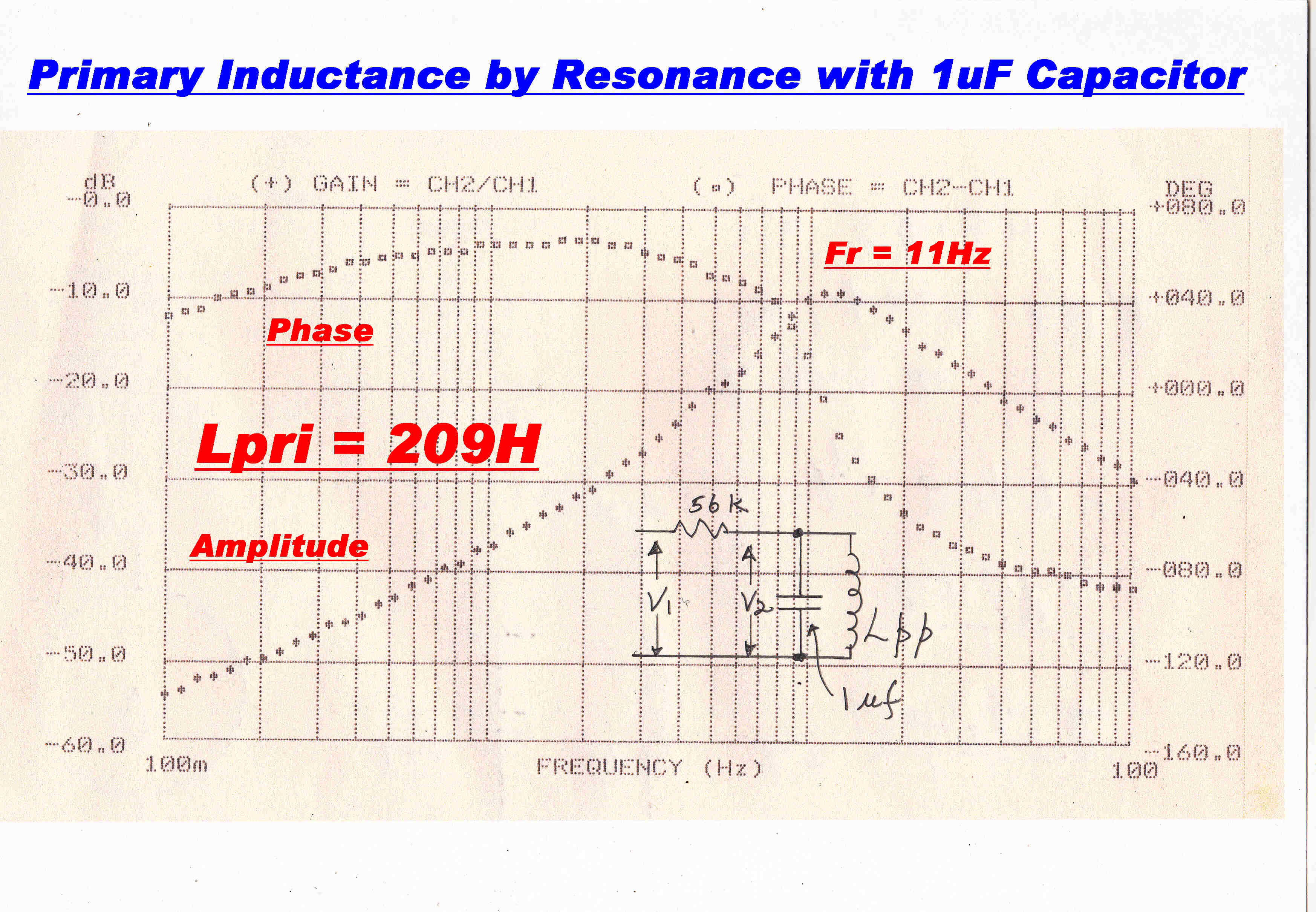
Low Frequency Measurements
The low frequency performance of the transformer depends on the magnetising inductance.
Since this is non-linear and varies with signal level, it presents problems both in measurement
and the design of low frequency loop stability.
Two different methods of measuring the low level magnetising inductance are shown below.
(A) In the first the low frequency response is plotted with the transformer terminated in its
nominal resistive load. Constant current drive is approximated by a high value resistor
in series with the primary.
(B) In the second method a large capacitor is paralleled with the primary inductance and
the resonant frequency measured.
|
|
|
As the frequency drops the magnetising current increases until it eventually
becomes a significant part of the current through the reflected load. |
Parallel resonance occurs at 11Hz. The amplitude response has
a maximum and the phase goes to zero. |
Transformer Steady State and Transient Response
To calculate the transformer response:-
(A) The transformer is treated as three mutually coupled inductors.
(B) The distributed capacity of the windings is treated as lumped
capacity across two halves of the split primary.

|

|
|
High Frequency Response |
The second order response of both halves of the primary exhibits a
peak with ringing at about 60KHz. |
Unbalanced Drive
In the analysis described above, it is assumed that the drive to the primary
is perfectly balanced.
This ideal may not occur in an amplifier, so it is of interest to evaluate
the response to unbalanced drives.
Current Drive to One Side of the Primary
The self capacity of the unenergised side of the primary is driven through the leakage reactance between the two halves of the primary: resonance may occur.
|
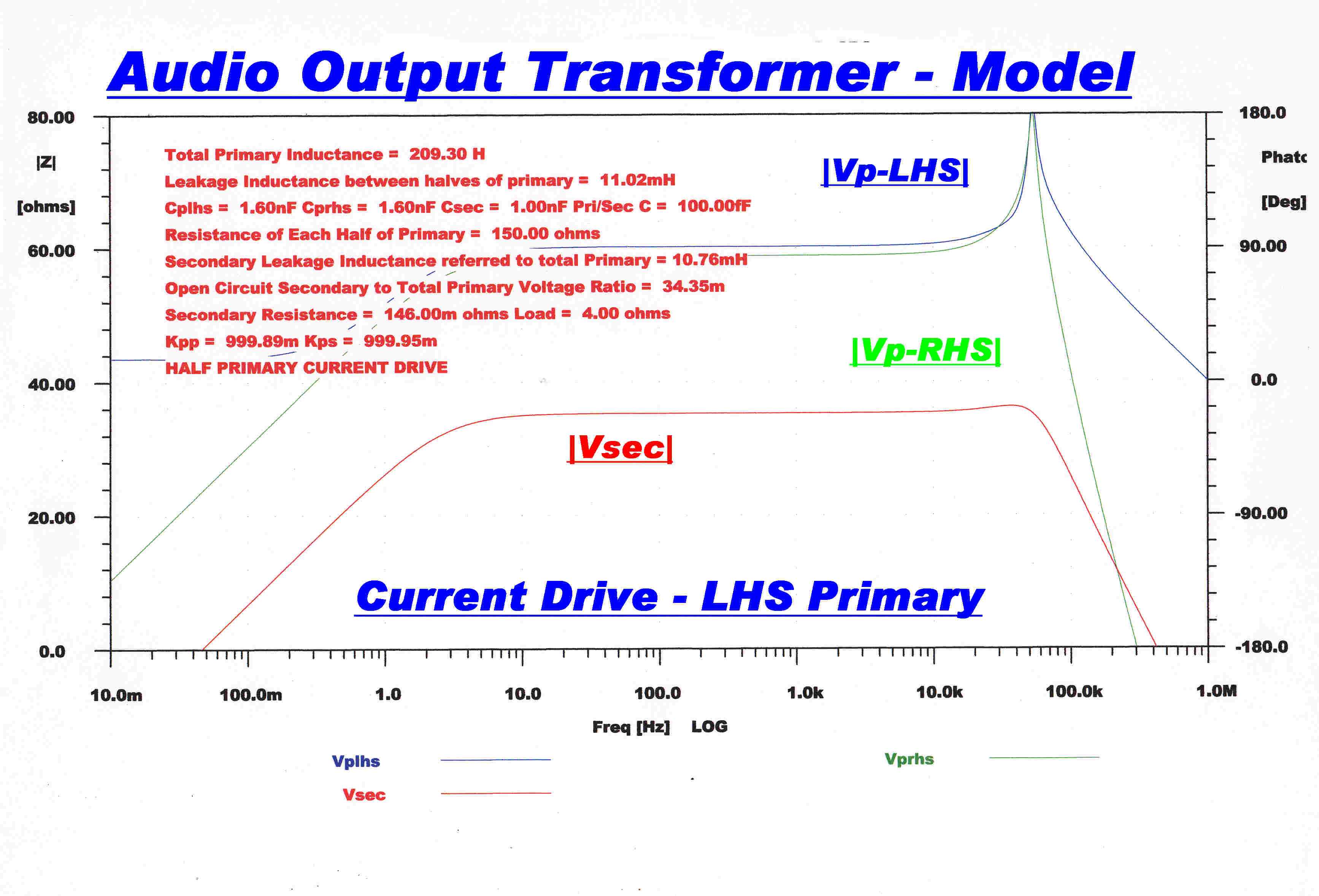
|
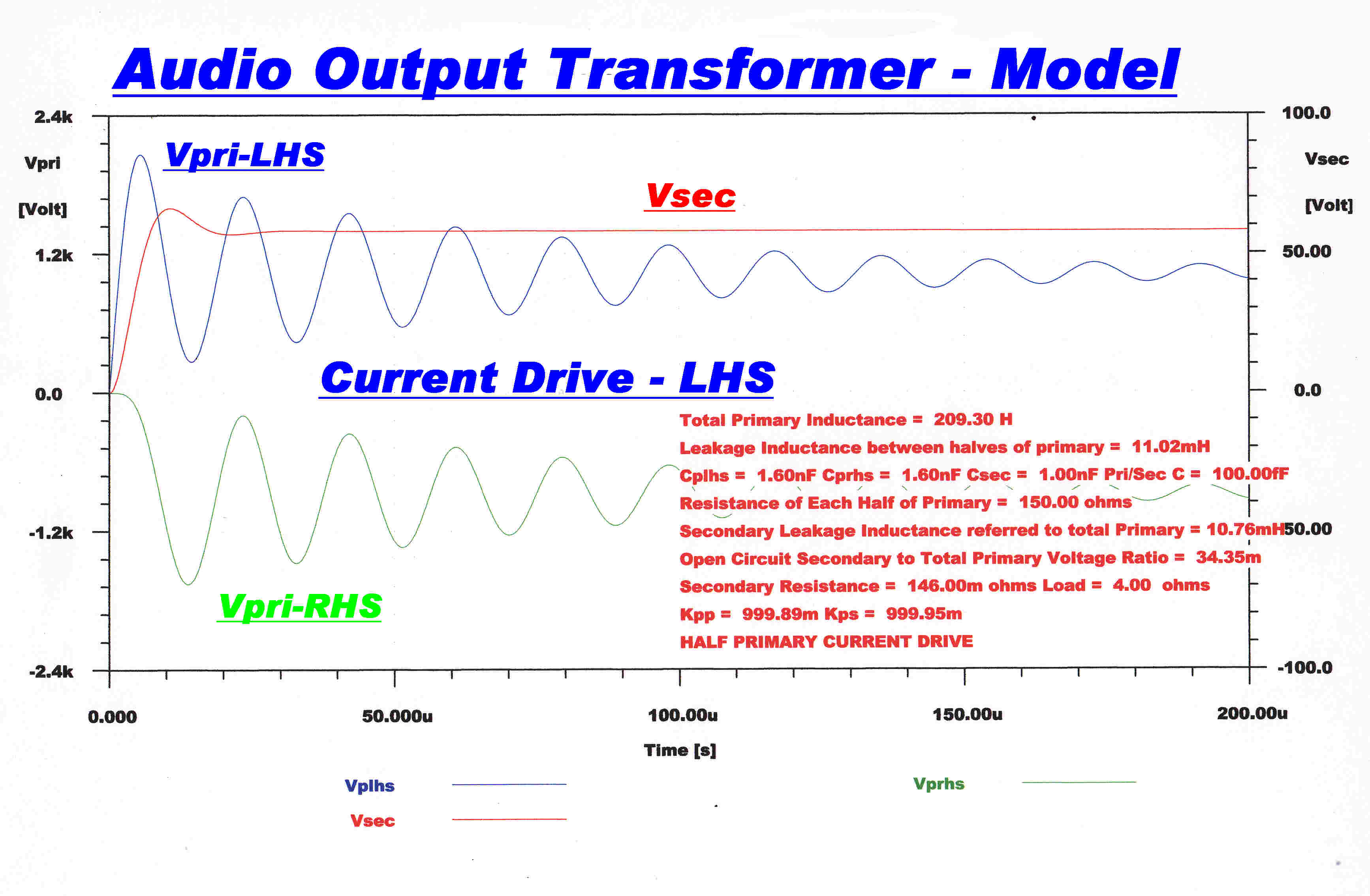
|
|
Steady State Response |
Steady State Response |
Step Function Response |
Voltage Drive to One Side of the Primary
The self capacity of the unenergised side of the primary is driven through
the leakage reactance between the two halves of the primary: resonance may occur.
In this case the primary leakage reactance and the primary self inductance form
a series tuned circuit to earth. This causes a dip at the resonant frequency.
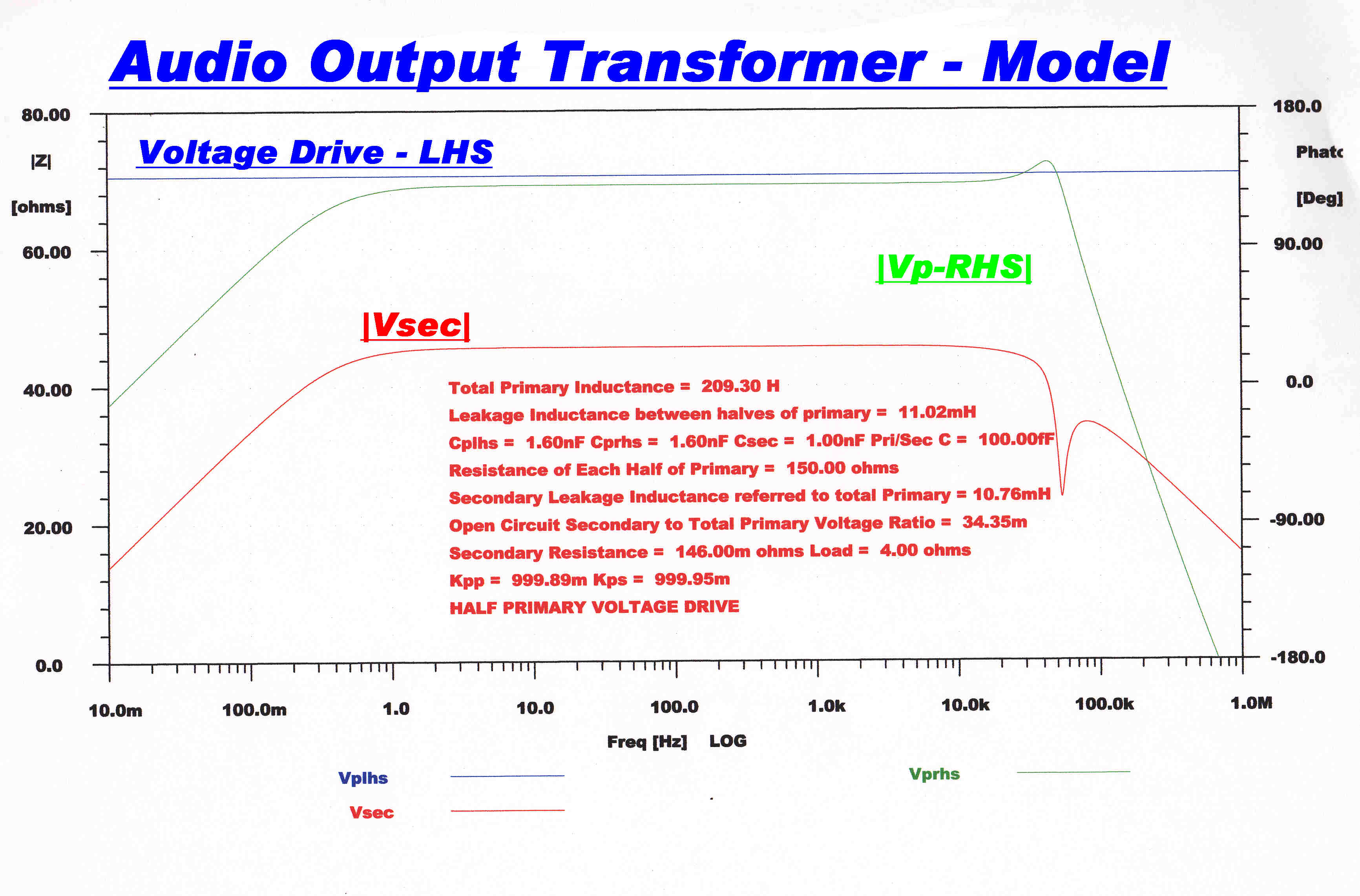
|
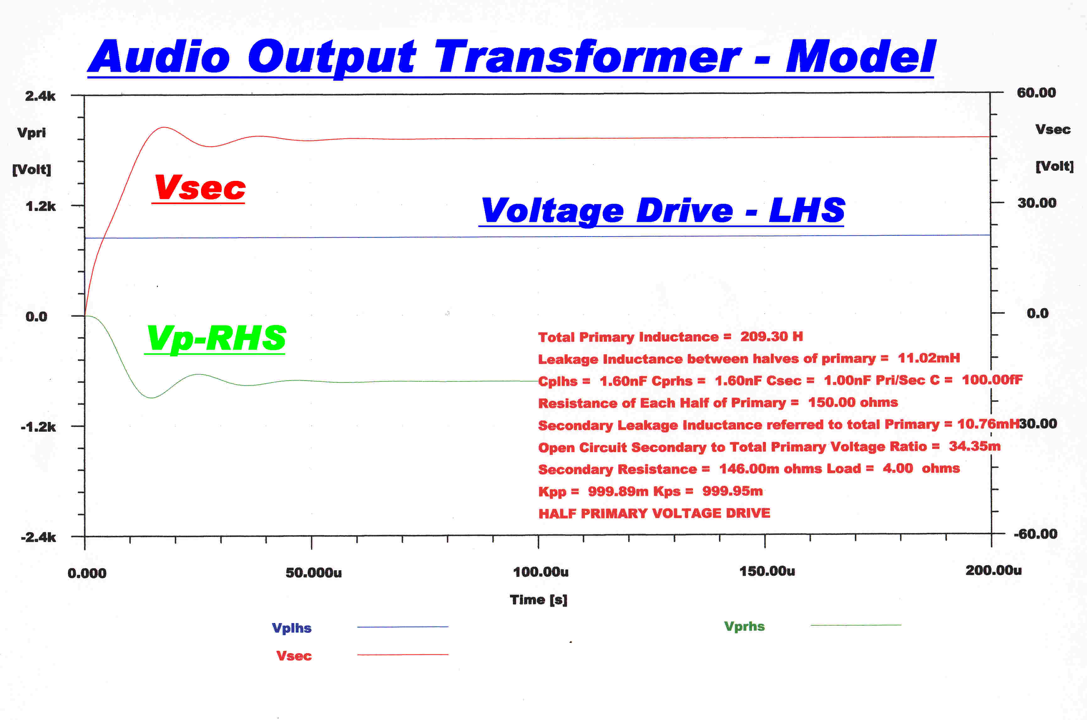
|
|
In the lumped transformer model, the input voltage generator
is now in parallel with the winding capacity of the driven side. |
The ultimate slope of 6db/octave in the primary - secondary transfer function
results in a finite slope at t = 0. |
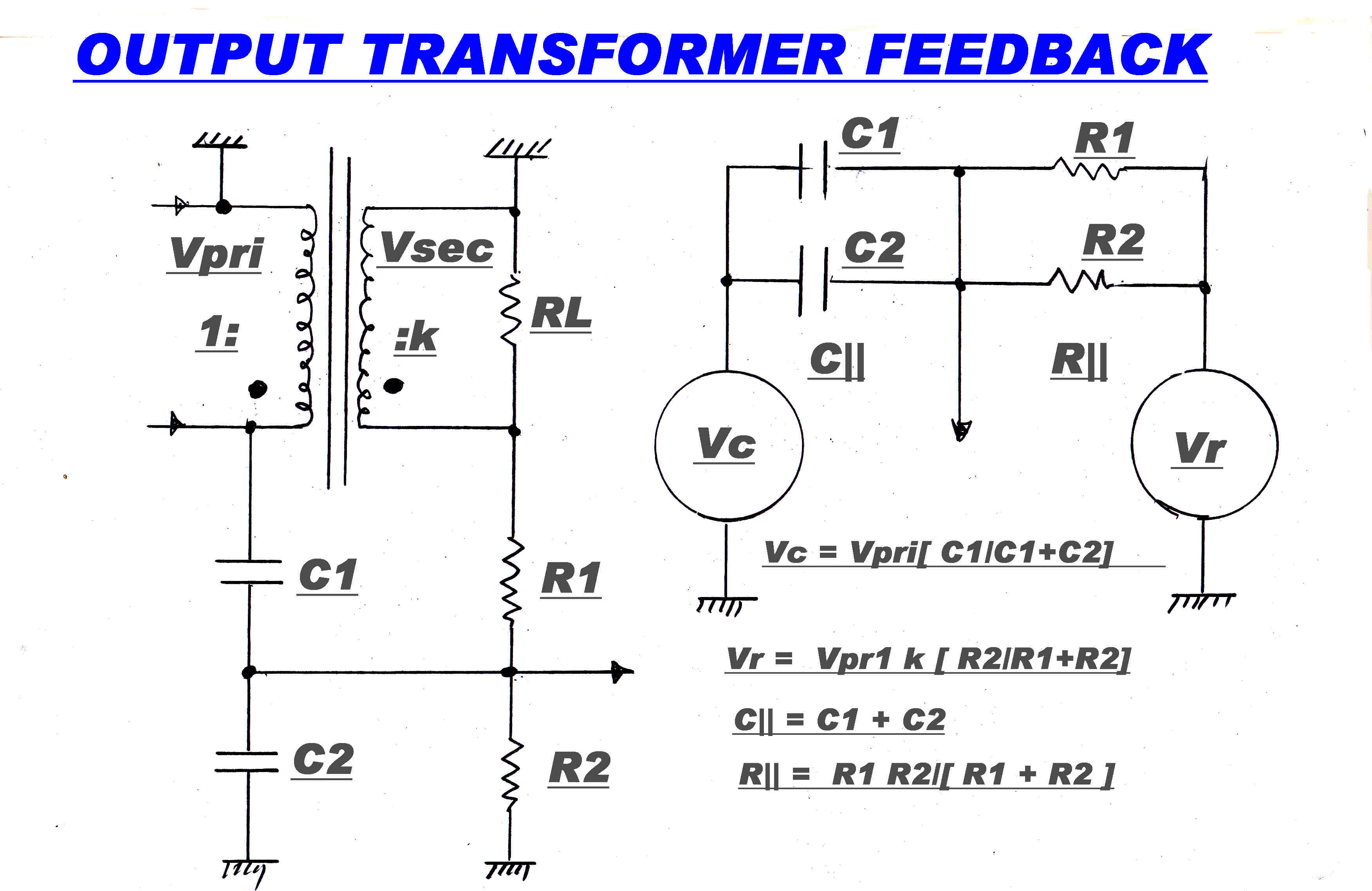
TRANSFORMER FEEDBACK NETWORK
It was pointed out above that the effects of leakage reactance of a transformer
are mitigated by current drive.
Unfortunately real life throws up a few problems with this.
[A] All the windings have self capacity and there is capacity feed through
between primary and secondary. Since there are now inductive and capacitive
parallel paths between primary and secondary, there is a possibility of cancellation
and the introduction of zeros into the transfer function.
[B] The load in the 100KHz range is highly indeterminate and usually highly inductive.
[C] Stubbing networks are placed across the primary of the transformer as a protection against
the generation of destructive peak voltages and the generation of parasitic oscillation.
These greatly reduce the transformer driving point impedance at high frequencies.
A network is therefore introduced so that the feedback signal comes from the secondary
of the output transformer for frequencies up to about 100KHz and above that from the primary.
The resulting increase in phase margin usually means that more feedback can be safely applied.
I was delighted when I developed this technique in the mid fifties, but somewhat deflated
to find after some time that Bell was well ahead of me.
The technique had been developed in the design of J type carrier amplifiers to overcome
the leakage inductance in the hybrid input and output coils.
See: Bell System Technical Journal January 1939 page 135
A Twelve-Channel Carrier Telephone System for Open Wire Lines
B W Kendell and H A Affel
 Let C// = C1 + C2
R// = R1R2/( R1 + R2 )
τ = R//C//
Let C// = C1 + C2
R// = R1R2/( R1 + R2 )
τ = R//C//
From inspection we can write:-
Vo = Vc τp/( 1 + τp ) + VR/( 1 + τp )
Let Vc = βV and Vr = ( β + Δβ )V
where β is the identical division ratio through the capacitive and resistive paths and
Δβ represents the error on the secondary due to leakage reactance etc.
We have then:-
Vo = βVτp/( 1 + τp ) + βV/( 1 + τp )
+ ΔβV/( 1 + τp )
= β/( 1 + τp ) + ΔβV/( 1 + τp )
Let the transformer voltage ratio Vsec/Vpri = k
Then β = C1/( C1 + C2 )
= kR2/( R1 + R2 )
Multiply each side by R1: we then have:-
C1R1 = k [ R1R2/(R1 + R2)]
[ C1 + C2 ]
= kR//C//
= kτ
So: C1 = kτ/R1 --------------(1)
But β = C1/( C1 + C2 )
So: C2 = C1( 1/β - 1 ) ------------(2a)
Or: C2 = (kτ/R1)( 1/β - 1 )----------(2b)
Now: β = k R2/(R1 + R2 )
So: R2 = R1/( k/β - 1 ) ------------(3)
Practical Values
For the output transformer: Rp-p = 3000ohms Rsec = 4ohms
Leakage Inductance between each half of primary: 11.14mH
Leakage Inductance Primary to Secondary ( Refered to total Primary): 13.98mH
Total Primary Inductance: 22.18H
Resistance of each half of Primary: 36 ohms
Resistance of Secondary: 0.16 ohms
Self Capacity of each half of Primary: 1000pF
From one side of the primary to centre tap (earth) Rp-ct = 750 ohms
For voltage ratio k - one side of primary to 4 ohm secondary:-
k = [Rs/Rpri]1/2 = [4/750]1/2
= 7.303x 10⁻²
For full output the voltage swing on one dide of the primary is 252 volts.
We need 1 volt peak delivered to the feedback network in the input stage. This will
give an overall sensitivity of 1 volt peak input for full power output.
So β = 1/252 = 3.96825x10⁻³
Now choose R1 so that it does not load the output significantly.
Put R1 = 4.7kohms.
From (3) we get R2 = 270 ohms.
We want to make the crossover frequency from secondary to primary somewhere between
90Khz and 100KHz. It turns out 91.3KHz gives preferred values for the capacities.
f
Substituting in (1) C1 = 27.1pF
Substituting in (2a) C2 = 6.8nF
The steady state and step function response for the transformer and feedback network
is shown below.
The total primary is driven from a constant current source:-
|
|
|
|
Low Frequency |
The front of the step function is shown. |
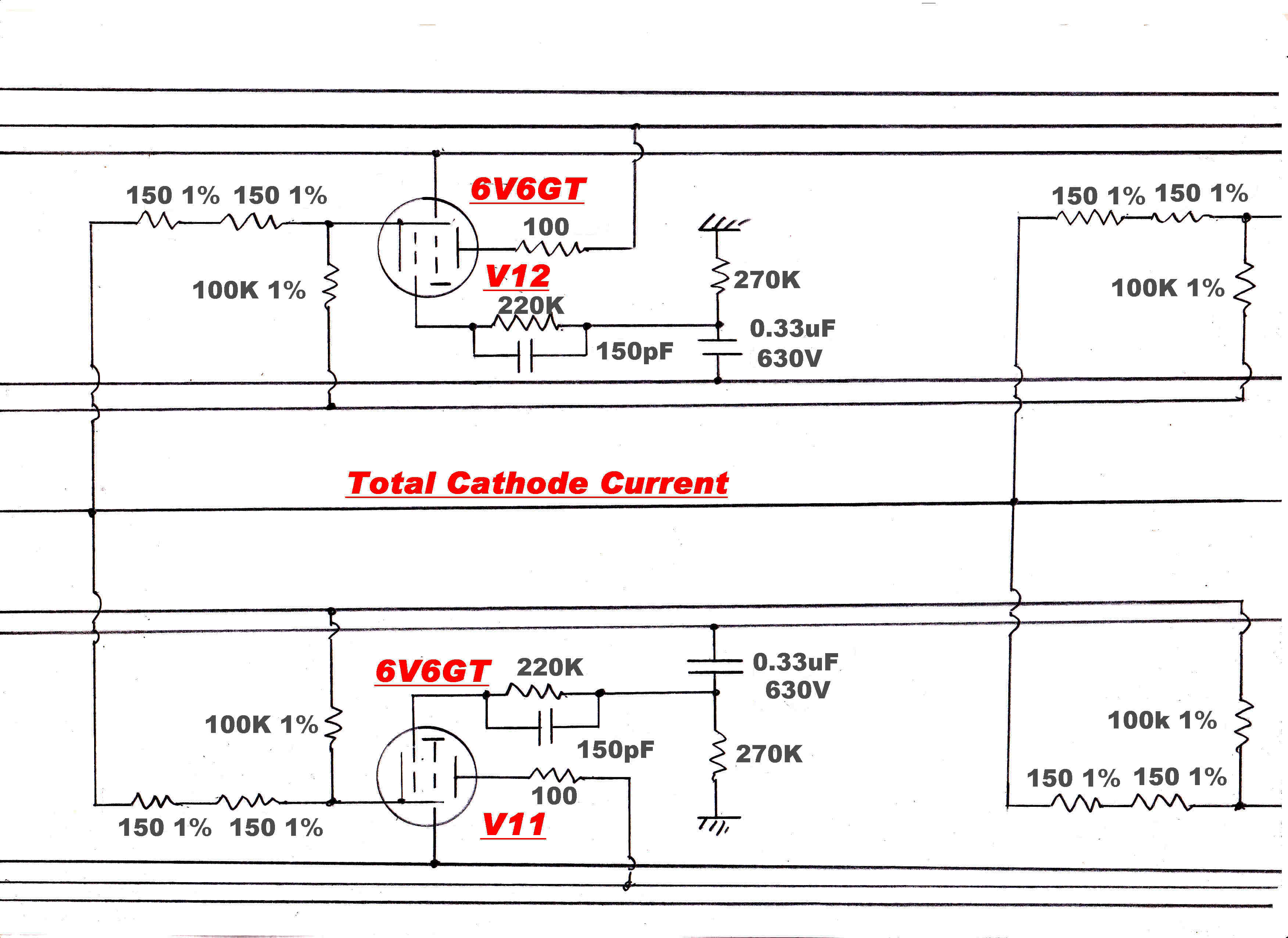
 A simplified circuit of the output stage current feedback is shown opposite.
The cathode current of the output 6V6 beam tetrodes is sensed by the cathode resistors
Rk1,Rk2,Rk3,Rk4 and summed by Ra1,Ra2,Ra3,Ra4.
Since the plate current provides the output, it must be the variable used for feedback.
The screen current is sensed by the resistor Rb and this voltage is subtracted from
the cathode feedback to give true plate current feedback.
The four 300 ohm cathode resistors combine to give a 75 ohm sensing resistor behind
the four summing resistors (25K ohm).
The sensing resistor Rb in parallel with Rs (2.2K) - the screen feed - gives a
75 ohm sensing resistor behind Rc (25K).
The open circuit output voltage at B will therefore give an accurate representation
of the total output current. This is subtracted from the input drive Vin to give
a feedback error signal on the grid (C) of the 6AC7 voltage amplifier.
The unbypassed cathode sensing resistors also improve the linearity of the output tubes.
The 6V6 with a cathode resistor may be treated as a tube with modified characteristics.
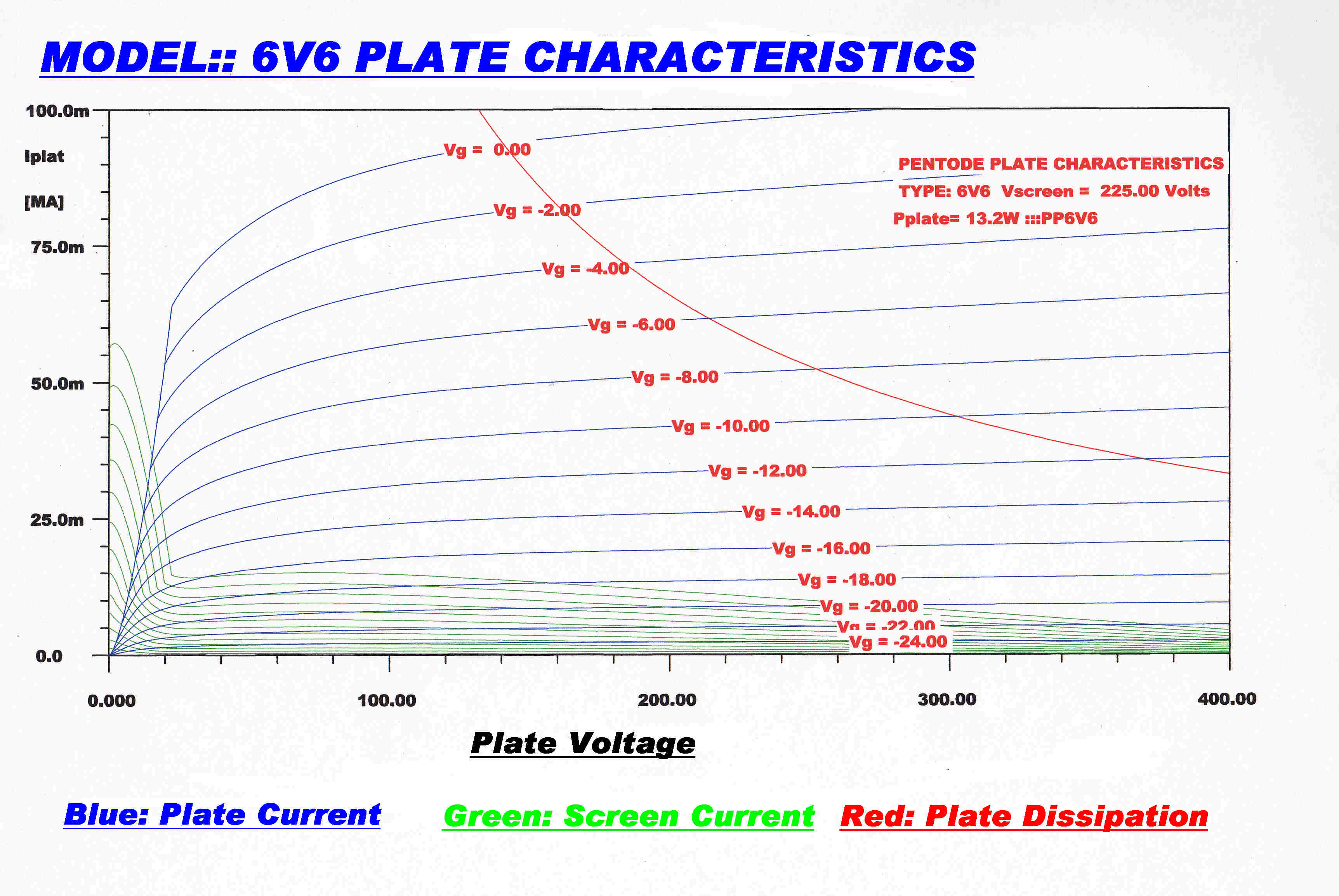
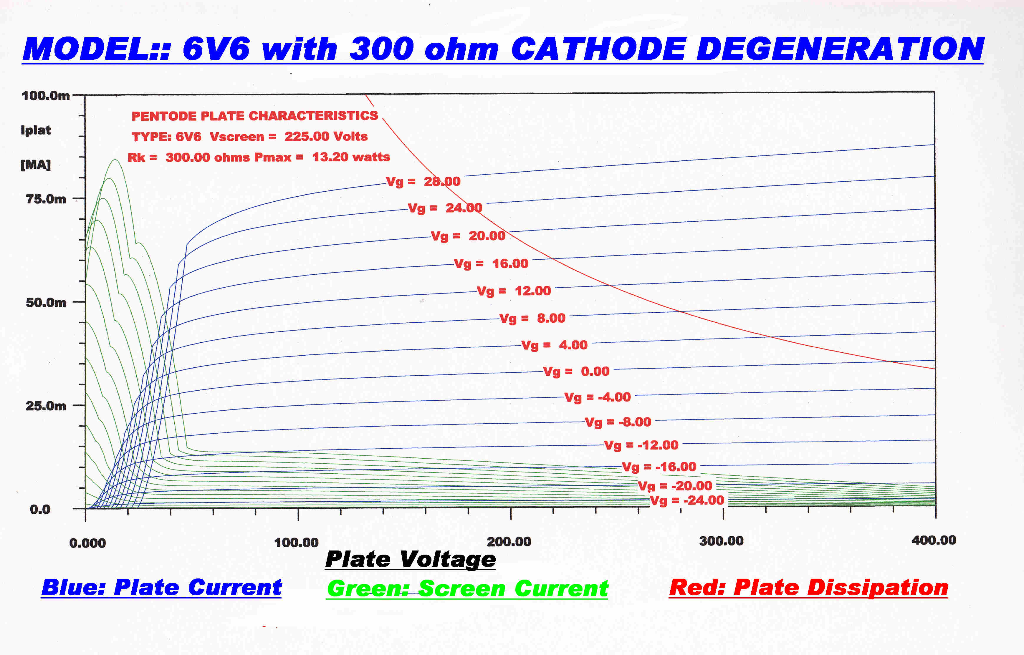
We can plot the characteristics of such a tube and compare it with the unmodified tube.
|
|
|
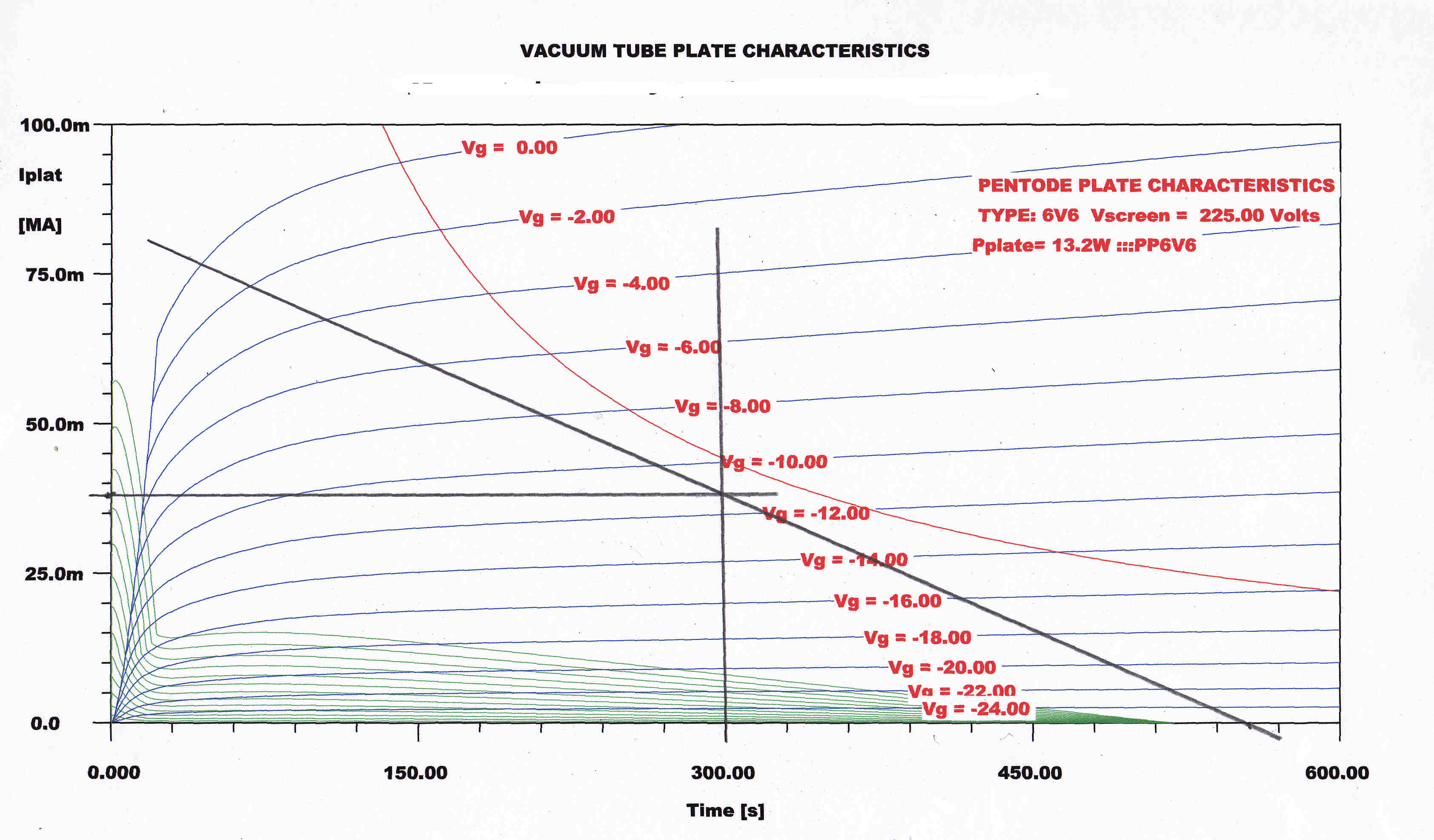
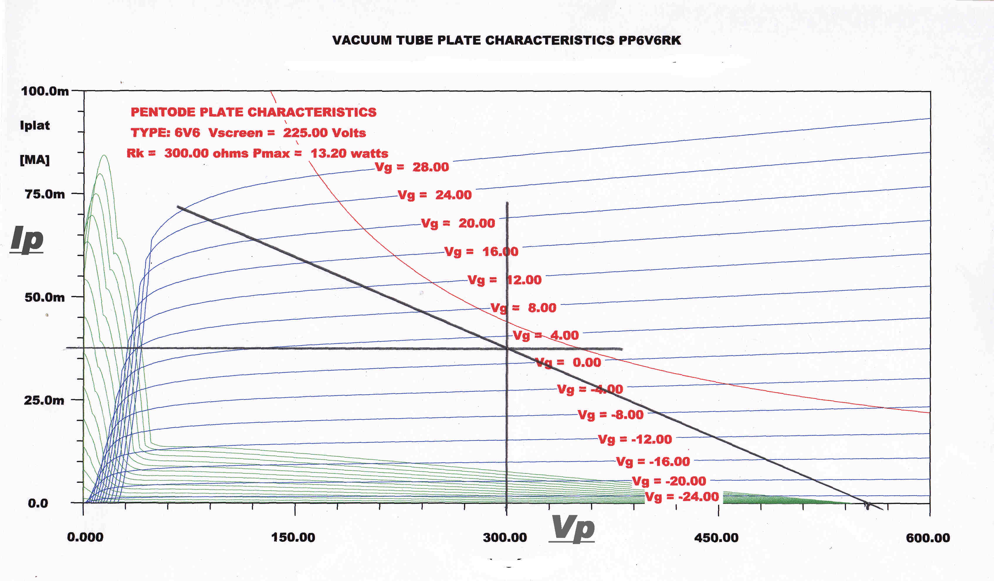
6V6 PLATE CHARACTERISTICS |
COMPOSITE 6V6 PLATE CHARACTERISTICS WITH 300 OHM CATHODE RESISTOR |
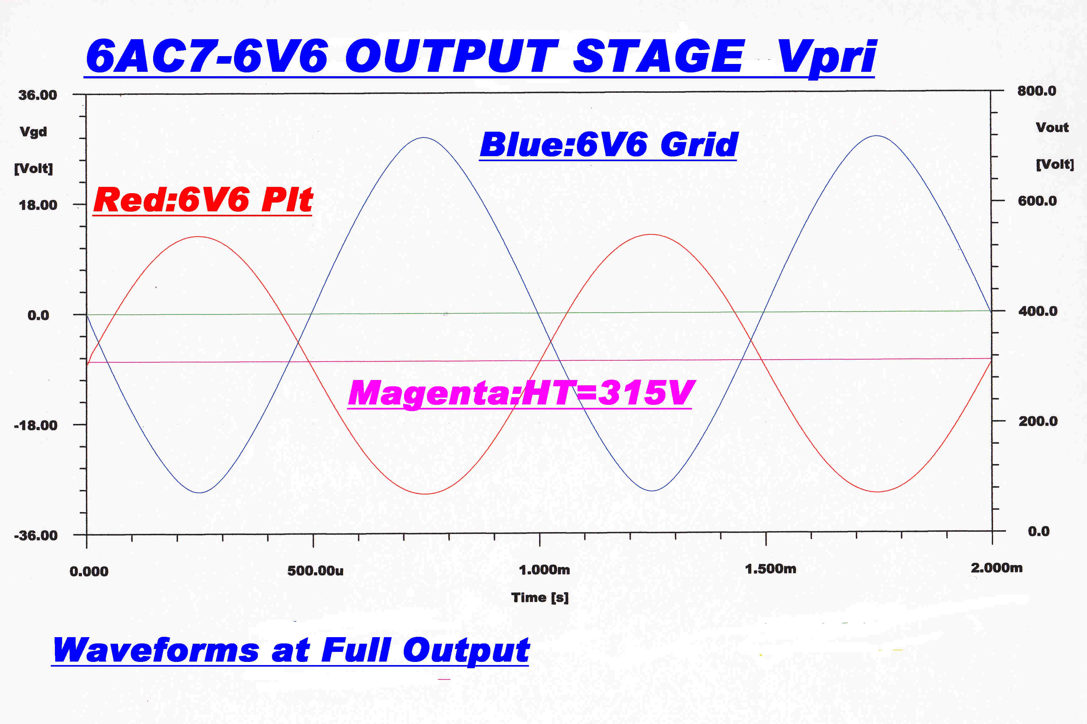
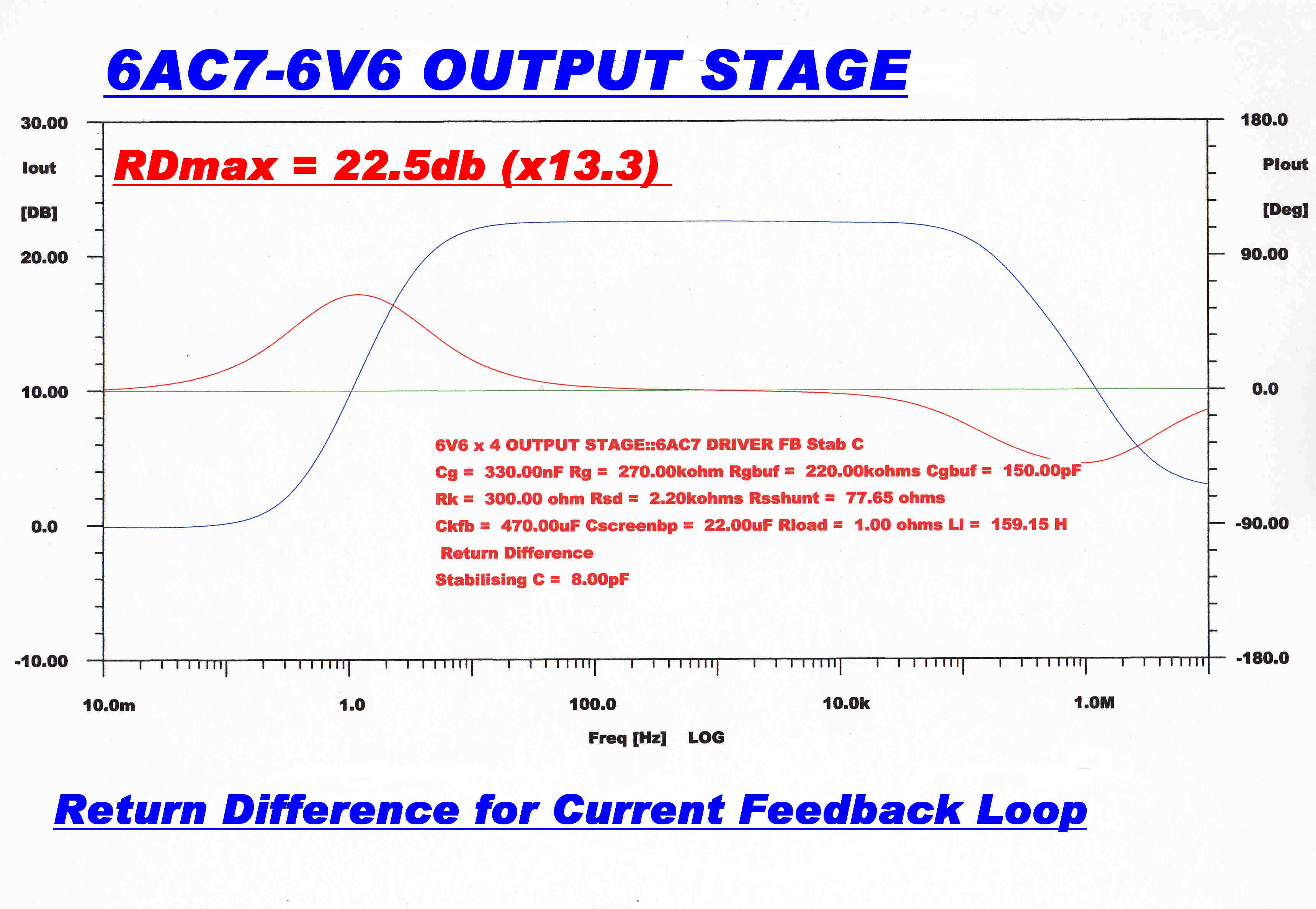
It will be shown that the return difference in the current feedback loop is 22.5db
or ( x13.3 ).
The feedback reduces the distortion by this amount by driving the grids of the 6V6s with
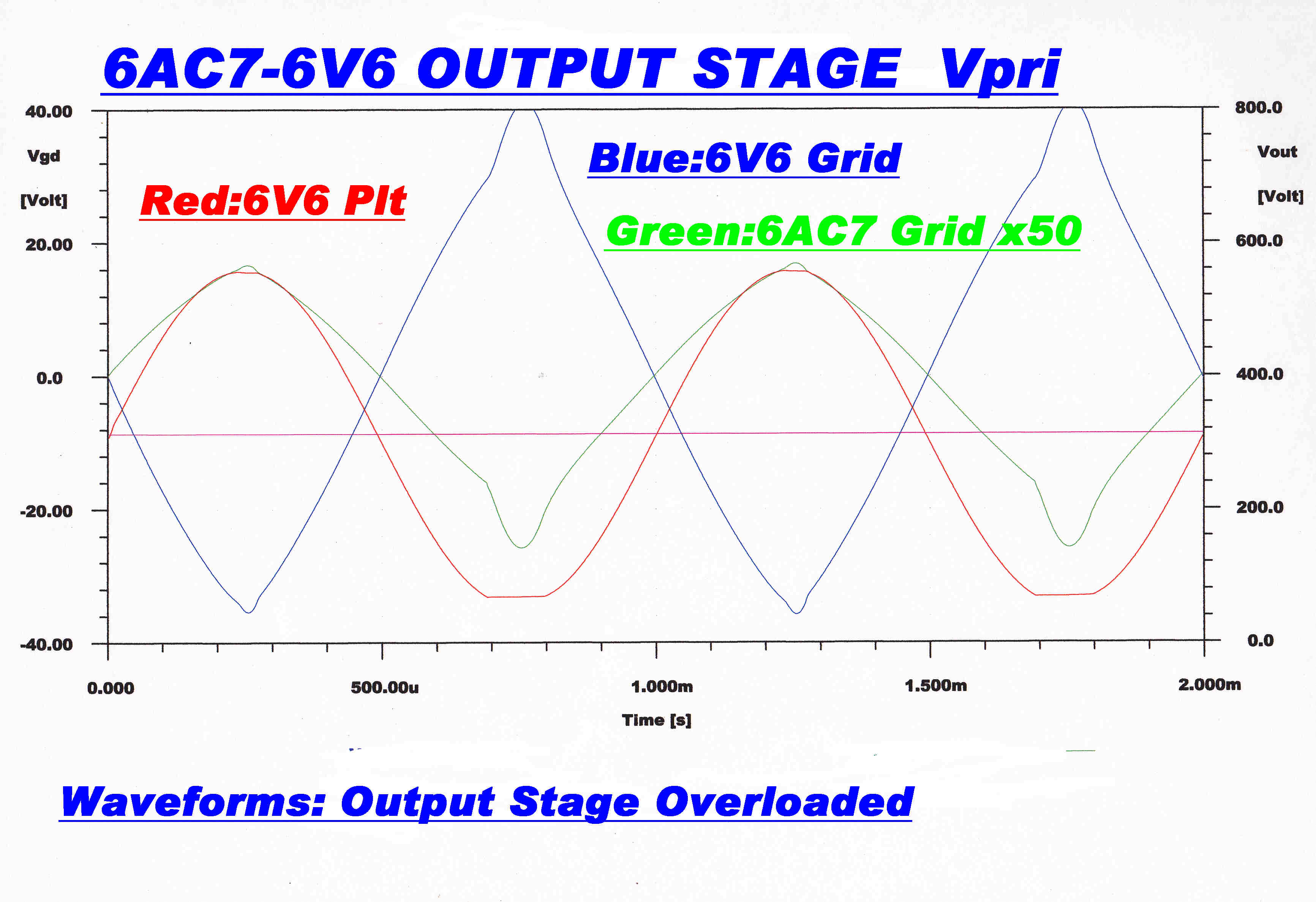
a distorted waveform. It is interesting to look at this waveform at full power output
for a sinusoidal input.
Because of the linearising effect of the cathode resistors, this waveform is
not all that far from sinusoidal.
|
|
|
6V6 PLATE and GRID DRIVE WAVEFORMS at FULL POWER OUTPUT |
6V6 PLATE and GRID DRIVE WAVEFORMS at OVERLOAD |
High Ffrequency
There are two dominant poles around the feedback loop. These are both on the real axis.
[1] The pole formed by the load resistance on the 6AC7 (17.43K) and the total capacity.
This consists of the stray C (estimated 15pF) and the input capacity of the 6V6s.
[2] The output resistance of the summing network (Ra1,Ra2,Ra3,Ra4,Rc ) and the input capacity
of the 6AC7 grid network.
Since the loop transfer function is second order, feedback can never produce instability.
Large amounts of feedback will produce peaks in the response as shown below.
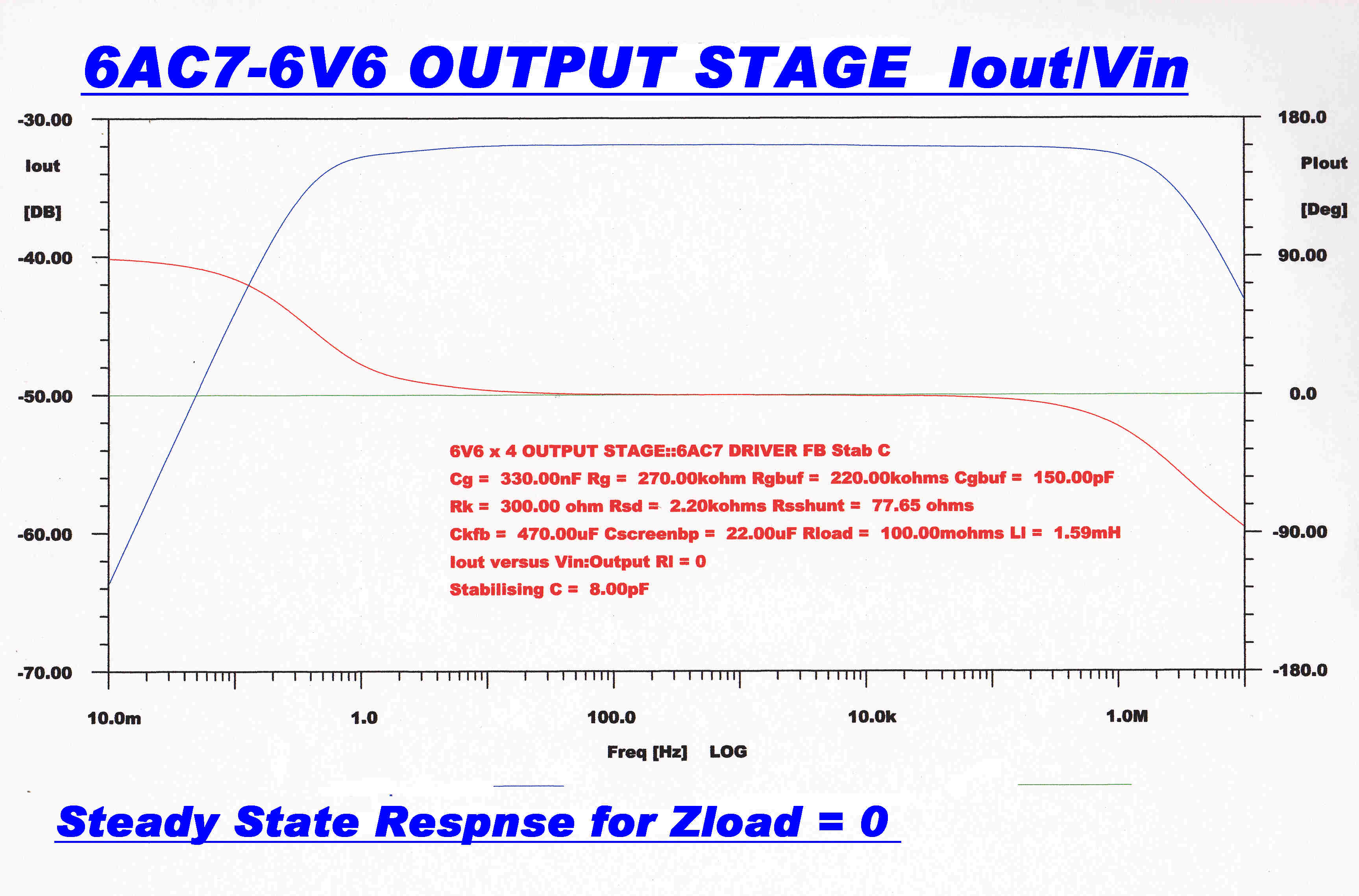
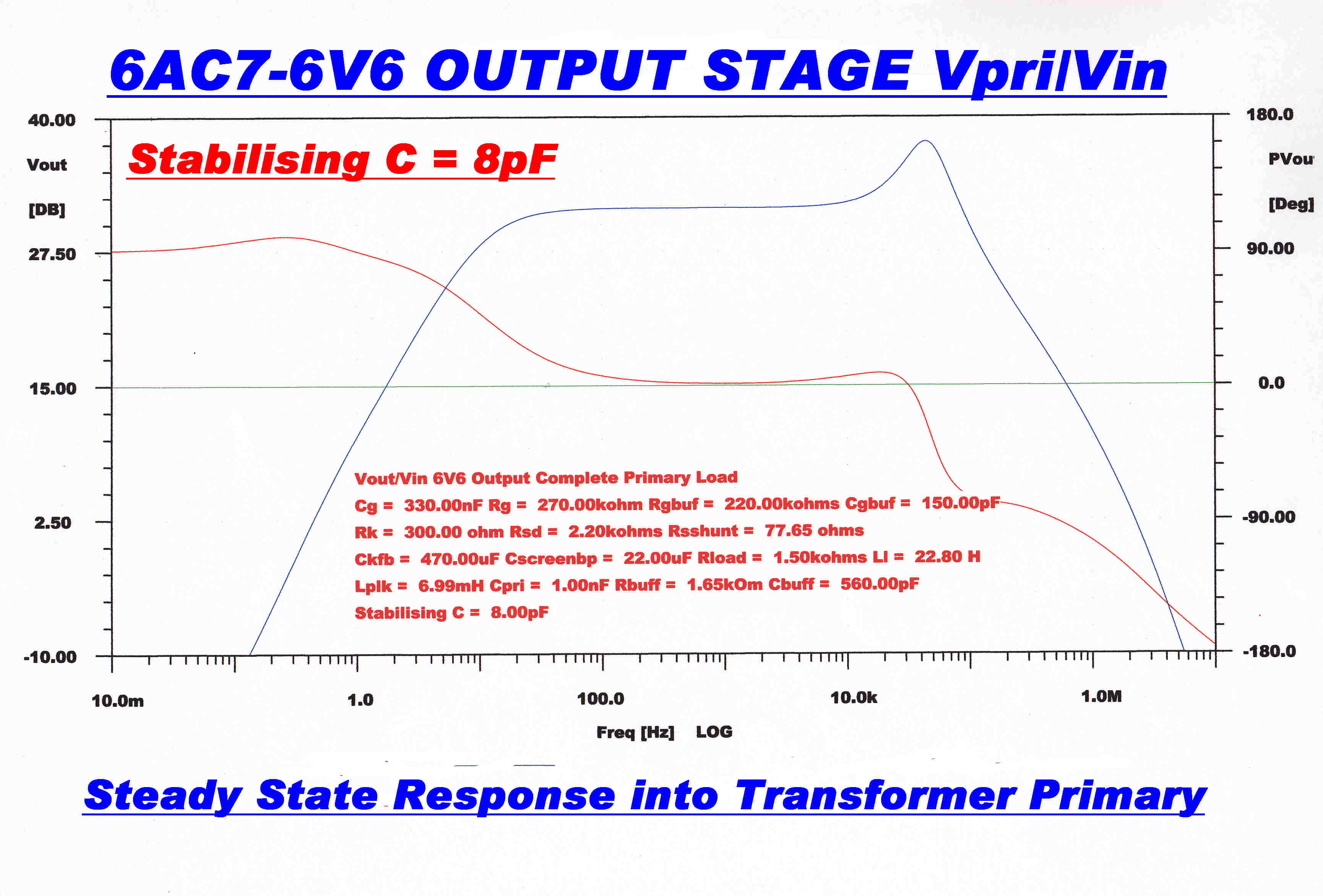
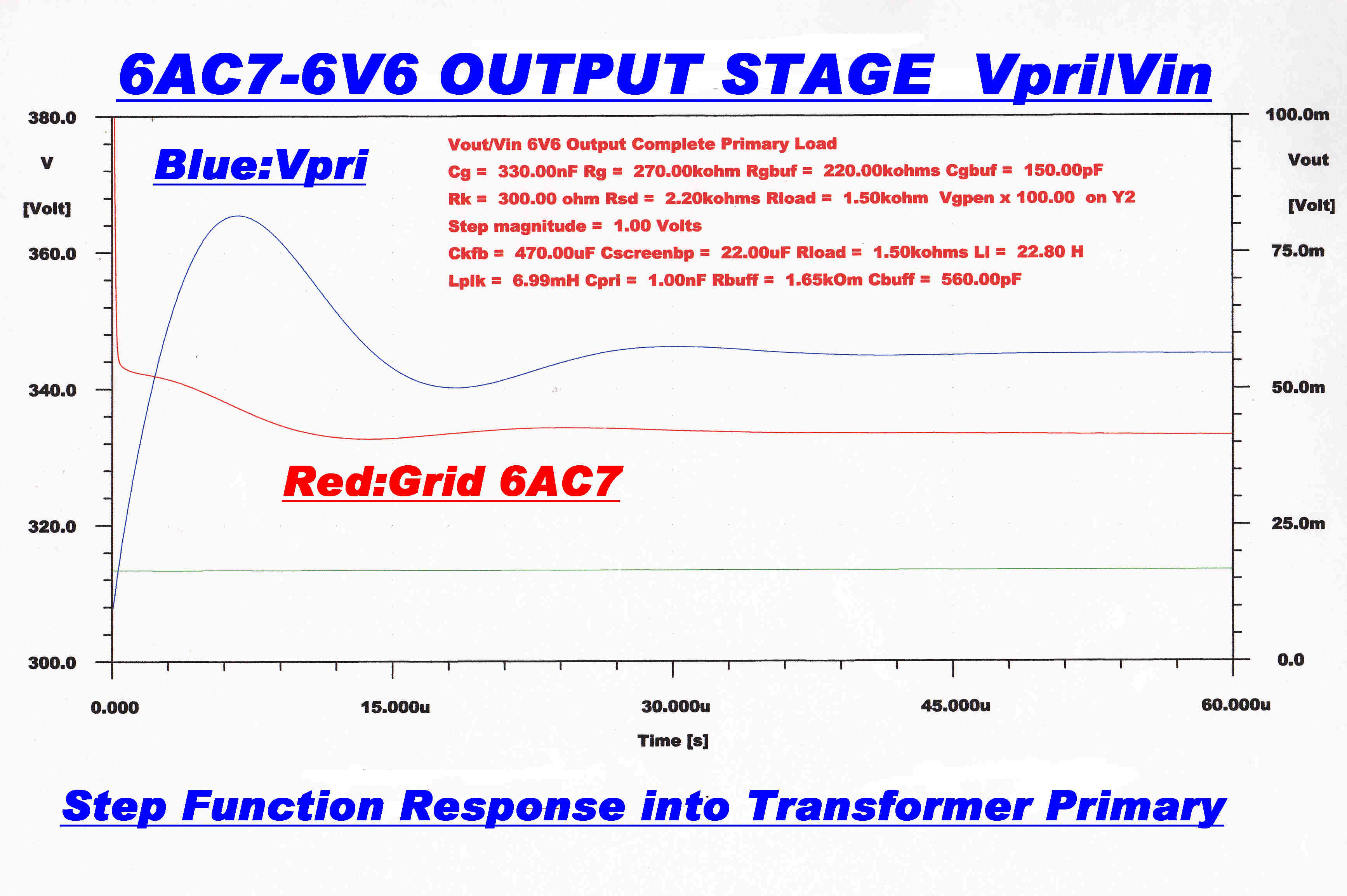
A closed loop monotonic response is obtained by adding the 8pF capacitor Cstab.
This effectively removes the second pole from the open loop transfer function. Its effect is
illustrated below.
Note: In the actual circuit the 8pF capacitor (5/15pF trimmer) is not connected to the plate of
the 6AC7 but to the grid side of a 0.33uF coupling capacitor.
This removes the high DC voltage from the trimmer.
Low Frequency
The coupling capacitors Cf, Cg1, Cg2, Cg3, Cg4 produce a second order low frequency
open loop transfer function. An extra pole and zero, producing a shelf, is added by
the 6AC7 cathode bypass capacitor Ck.
The time constants are staggered to give a closed loop response without a peak.
This is illustrated below.
|
|
|
CURRENT FEEDBACK LOOP::NO STABILISATION |
CURRENT FEEDBACK LOOP::WITH 8pF STABILISATION |
|
|
|
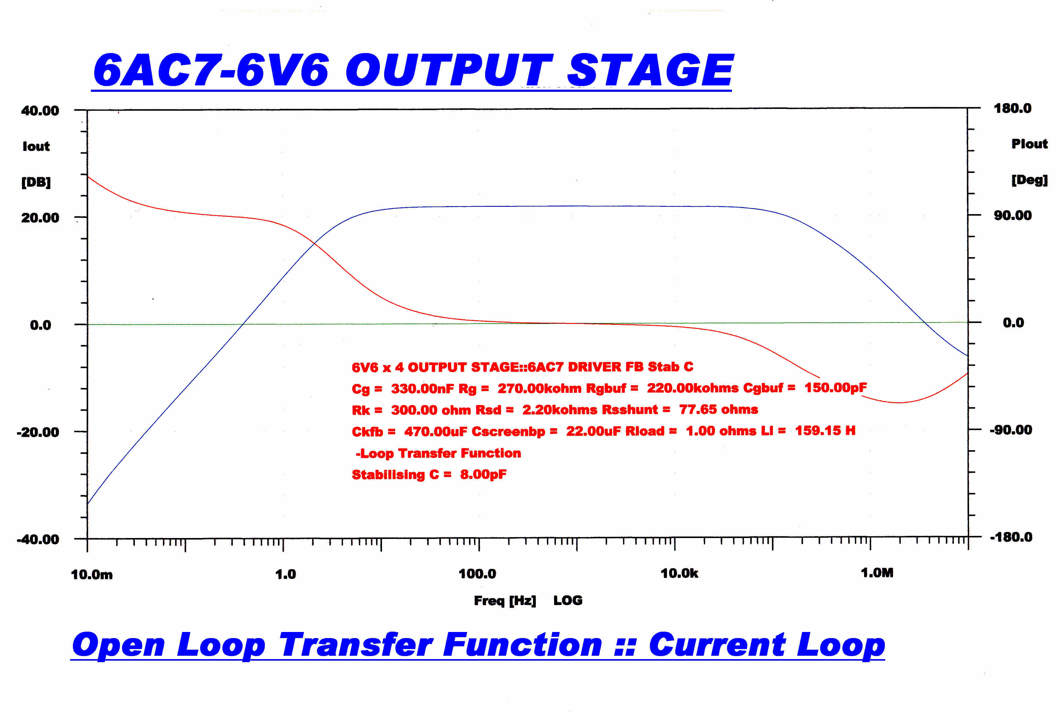
OPEN LOOP TRANSFER FUNCTION |
RETURN DIFFERENCE : CURRENT LOOP |
The self capacity of the primary winding is distributed.
It is represented here as a lumped capacity so the results are
only approximate.
The primary impedance is further modified by an R-C "snubbing" network in parallel.
The overall response to the primary is shown below.
|
|
|
STEADY STATE RESPONSE OF OUTPUT STAGE INCLUDING TRANSFORMER |
STEP FUNCTION RESPONSE OF OUTPUT STAGE INCLUDING TRANSFORMER |
 The output impedance of power supplies at low frequencies provides unwanted coupling
between stages via the high tension line.
The output impedance of power supplies at low frequencies provides unwanted coupling
between stages via the high tension line.
The feedback loops induced by this unintended coupling may be unstable and reult in violent low
frequency oscillation. This effect is commonly termed "motor-boating" because of its characteristic
sound in a loud speaker.
Battery powered vacuum tube receivers were prone to the effect as the internal resistance
of the B battery increased with age.
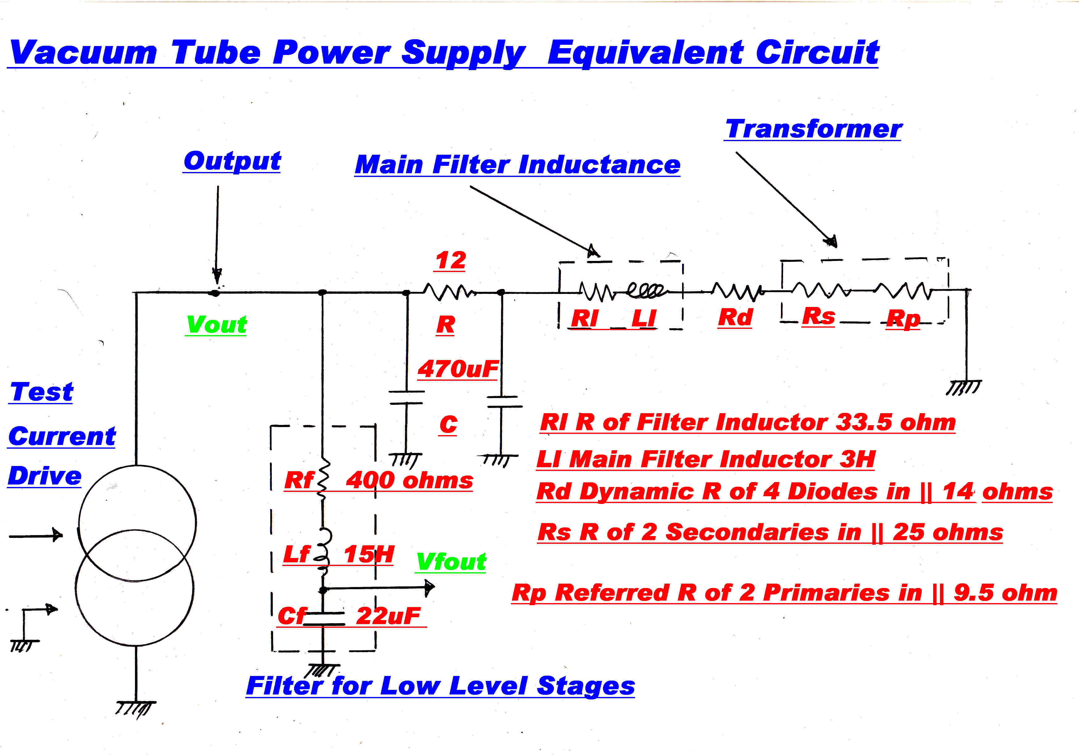
The equivalent circuit of the power supply for the 6V6 vacuum tube amplifier is shown opposite.
The low level input stage high tension is fed from an L-C filter to further reduce the 100Hz. hum level
on the HT line. This corresponds with the Vfout output. The 6V6 output stages are fed from the Vout
output.
The equivalent circuit is shown with a constant current drive test generator for evaluating
output impedance and transfer impedance to the front end stages.
|
|
|
STEADY STATE RESPONSE OF POWER SUPPLY OUTPUT IMPEDANCE : TRANSFER IMPEDANCE |
STEP FUNCTION RESPONSE OF POWER SUPPLY OUTPUT IMPEDANCE : TRANSFER IMPEDANCE |
At frequencies below about 2 Hz the output impedance and transfer impedance
equal 94 ohms with a phase angle close to zero.
The 470uF filter capacitors cause the output impedance to approach zero at high
frequencies with a phase angle of -90 degrees.
Resonance in the front stage L-C filter makes the modulus of the transfer impedance
greater than that of the output impedance over the range 2Hz to 12Hz, with the greatest
increase at about 8HZ. The ultimate phase change is 270 degrees.
The low level stage filter therefore increases the common mode feedback and is
a destabilising influence.
The output stages on each side of the push-pull amplifier act as a current generator.
The Gm of each side from the output of the phase splitter to the transformer primary is
24.83MA/V. The common mode Gm-cm is therefore 2x24.83MA/V = 49.66MA/V ≈ 50MA/V.
The loop gain, Aht, from the driver input of the output stage to the input stage HT
is given by:-
Aht = 2 Gm Zt
Up to about 2Hz |Zt| = 94 ohms , so Aht = 4.7.
We depend on the common mode rejection of the input stage, together with the low frequency
attenuation in the coupling networks, to reduce the overall loop gain to much less than 1.
HIGH TENSION TRANSIENT REJECTION
HIGH FREQUENCY CASE
 In any pentode stage with a resistive load, the output due to high tension transients
can be suppressed by feed forward of a fraction of the high tension transient into the screen
voltage.
In any pentode stage with a resistive load, the output due to high tension transients
can be suppressed by feed forward of a fraction of the high tension transient into the screen
voltage.
A simplifiesd circuit to achieve this is shown opposite.
At high frequencies XCk ≈ 0, so the cathode of the pentode may be shown as earthed
for signals.
Without any correction:-
ΔVout = ΔVht
Rp/( Rp + RL )
where:- Rp = plate resistance of pentode
RL = load resistance
The correction signal is attenuated in the capacitive divider C1, C2 and applied to the screen,
where it produces an increase in plate current and so an output of opposite sign.
Here ΔVout = - [C1/(C1 + C2)][ Acf]
[(Gm g-pRL)/μsg]
For zero output the magnitude of these two signals must be equal so:--
C1 = C2/[( 1 + RL/Rp) Acf Gm gp
RL / μsg - 1 ]
Here:-
RL/Rp < < 1
For the 6SJ7 input stage:-
C2 = 1uF
Cathode Follower Gain Acf = 0.995
Mutual Conductance Grid - Plate : Gm g-p = 1.23MA/V
Load Resistance : RL = 56K
Amplification Factor Screen - Grid : μsg = 12.3
So C1 = 0.219uF.
LOW FREQUENCY CASE
 At very low frequencies Xck > > Rk
so that the cathode degeneration provided by Rk
reduces the effective Gm g-p of T1.
The drive to the screen must be increased,
the attenuation in the capacitive divider C1, C2 reduced, and C1 increased
by Δ C.
Let β = Is/Ip
where: Is = screen current and Ip = plate current.
For the 6SJ7 input stage β = 0.31
Then the mutual conductance between grid and cathode, Gm g-k, is given by:-
Gm g-k = Gm g-p( 1 + β )
Applying Thevenin, the total resistance in the cathode Rtot is now given by:-
Rtot = 1/Gmg-k + Rk
= [ 1 + Gmg-k Rk ]/Gmg-k
Let the reduced Gm be GT
Then GT = 1/Rtot =
Gmg-k / [ 1 + Gmg-k Rk ]
Cathode degeneration has decreased the gain by a factor K where:-
K = [ 1 + Gmg-k Rk ]
= [ 1 + Gmg-p( 1 + β) Rk ]
With the reduced gain of cathode degeneration, we now have:-
C1 + ΔC = C2/[( 1 + RL/Rp) Acf
Gm gp RL / (μsg
(1 + Gmg-p( 1 + β) Rk ) ) - 1 ]
Substituting: C1 + ΔC = 2.33uF: ΔC = 2.11uF
Note that for full compensation of cathode degeneration to be possible:-
( 1 + RL/Rp) Acf
Gm gp RL / (μsg
(1 + Gmg-p( 1 + β) Rk ) ) > 1
GENERAL CASE : FULL TRANSIENT COMPENSATION
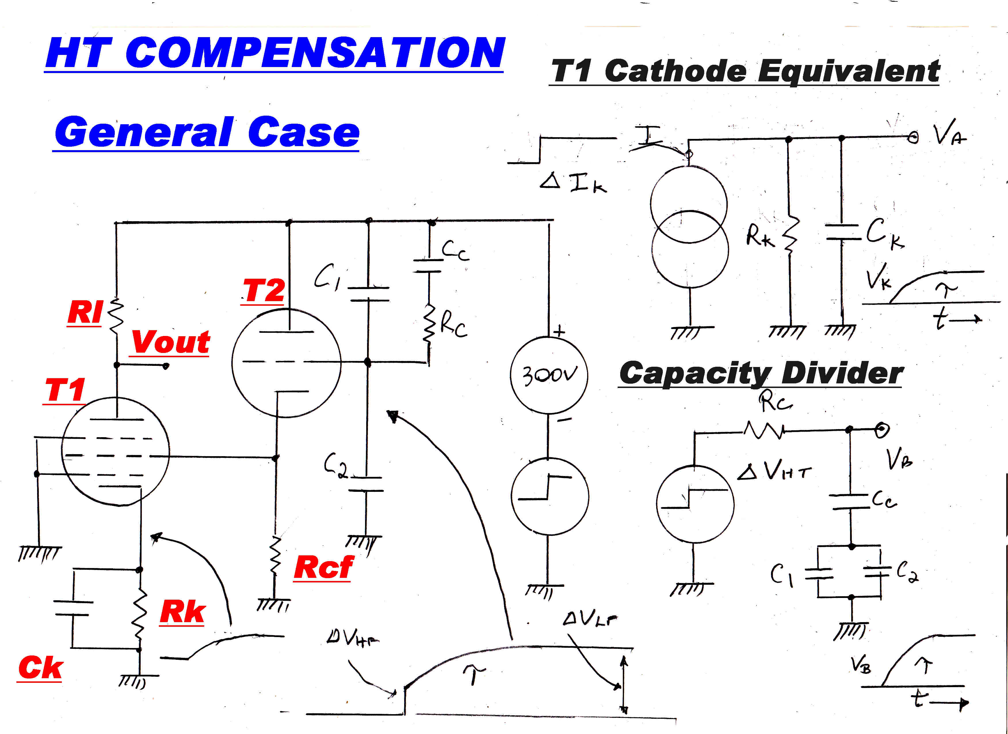 The plate current increment of T1 must be a step function for full
transient compenstion.
The plate current increment of T1 must be a step function for full
transient compenstion.
This will produce an exponential rise in voltage on the cathode as shown of the form:-
v = ΔV( 1 - e-t/Tk )
where Tk = RkCk = 470uFx1.8K = 0.846S
The equivalent circuit of the voltage divider in the grid of T2 is as shown.
This will also produce a transient given by:-
v = ΔV( 1 - e-t/TD )
Here Cc = 2.11uF: C1 = 0.219uF: C2 = 1uF
So Ctot = 0.773uF
For full compensation Tk = TD : so Rc = 1.095Meg.
COMPUTER SOLUTION PERTURBATION OF HIGH TENSION
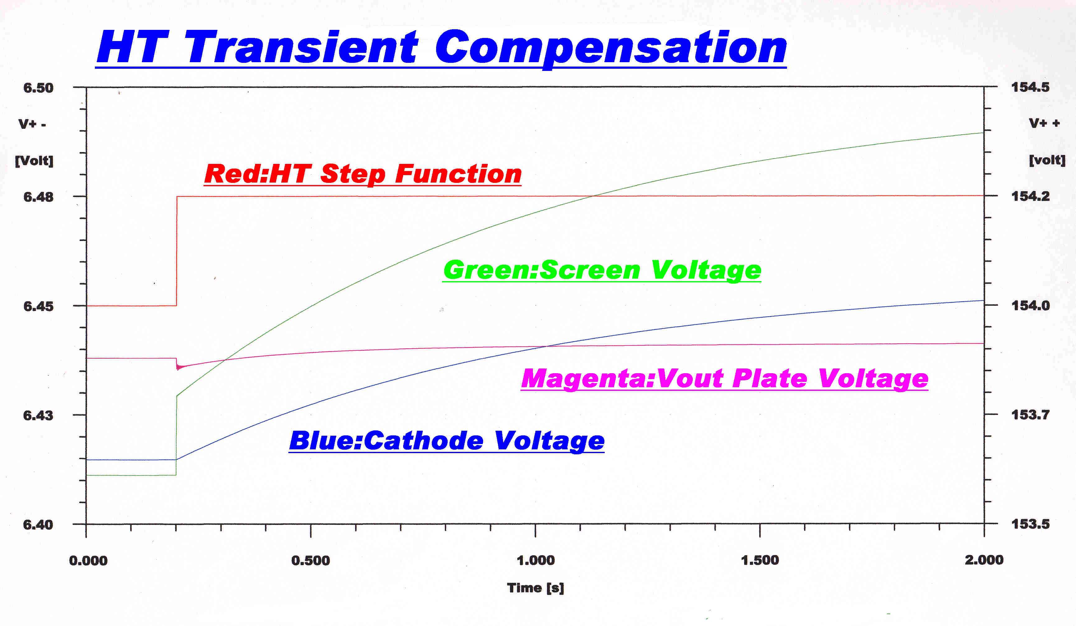 The output from the plate of the first (6SJ7) stage for a 1 volt step function of
high tension voltage is showm on an expanded voltage scale.
The output from the plate of the first (6SJ7) stage for a 1 volt step function of
high tension voltage is showm on an expanded voltage scale.
Except for a small initial error, the transient is suppressed. The initial error is due to
complex loading on the cathode follower output not included in the above analysis.
The pentode cathode and cathode follower grid waveforms are as predicted.
FULL CIRCUIT DIAGRAM
|
|
|
|
|
|
|
|
|
|
|
|
|
|
|
|
|
|
|
|
|
|
|
|
The plate characteristics plotted from the computer model are shown below.
|
|
|
|
6AC7 Wide Band Pentode |
6SJ7 Low Noise Pentode |
6SN7 Low μ Triode |
INPUT AND PHASE SPLITTER STAGES
The circuit of the input and phase splitter stages in a form suitable for digital
computation is given below.
Several small ( 1 ohm ) resistors such as R22f, R23f have been added to aid convergence.
If these resistors are not present, then C14f and C15f form a capacitive load across
the step function voltage generator Vtf, giving rise to infinite initial currents
and non-convergence.
If R5f = 100Meg ohm then VT1f and VT2f are cathode coupled via C3f, C4f.
Putting R5f to 1 milliohm reduces this coupling to virtually zero.
The voltage generator V
The voltage generator Vtf perturbs the high tension to calculate the
sensitivity to high tension transients.
|
Note: |
|
|
TUBE OPERATING CONDITIONS
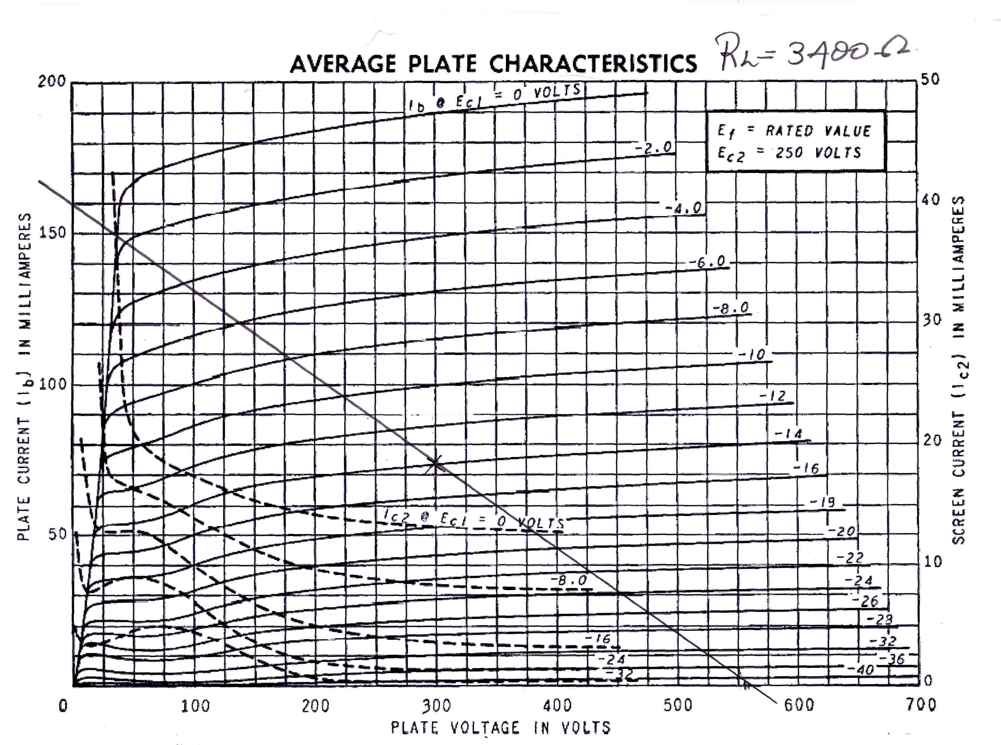
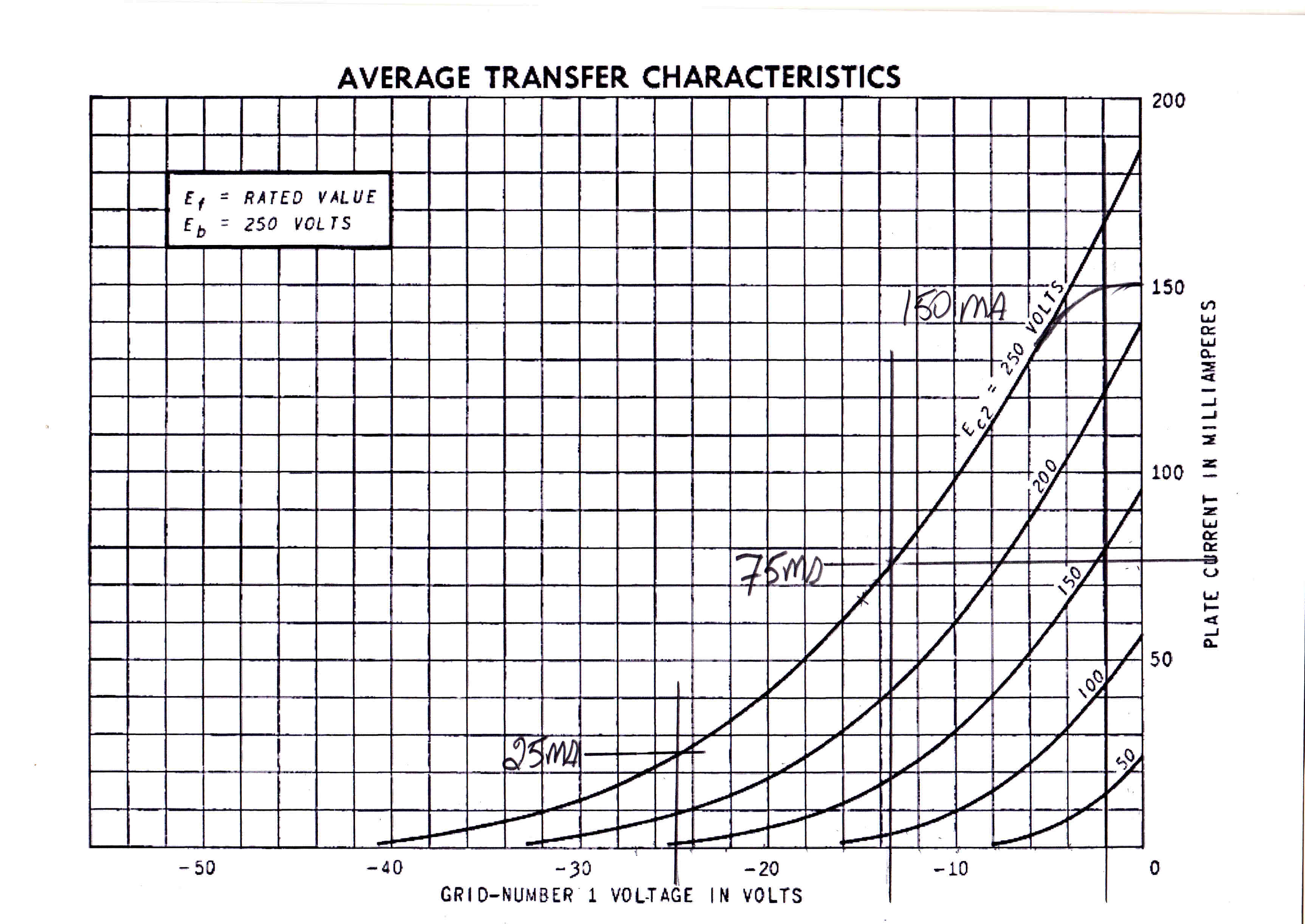
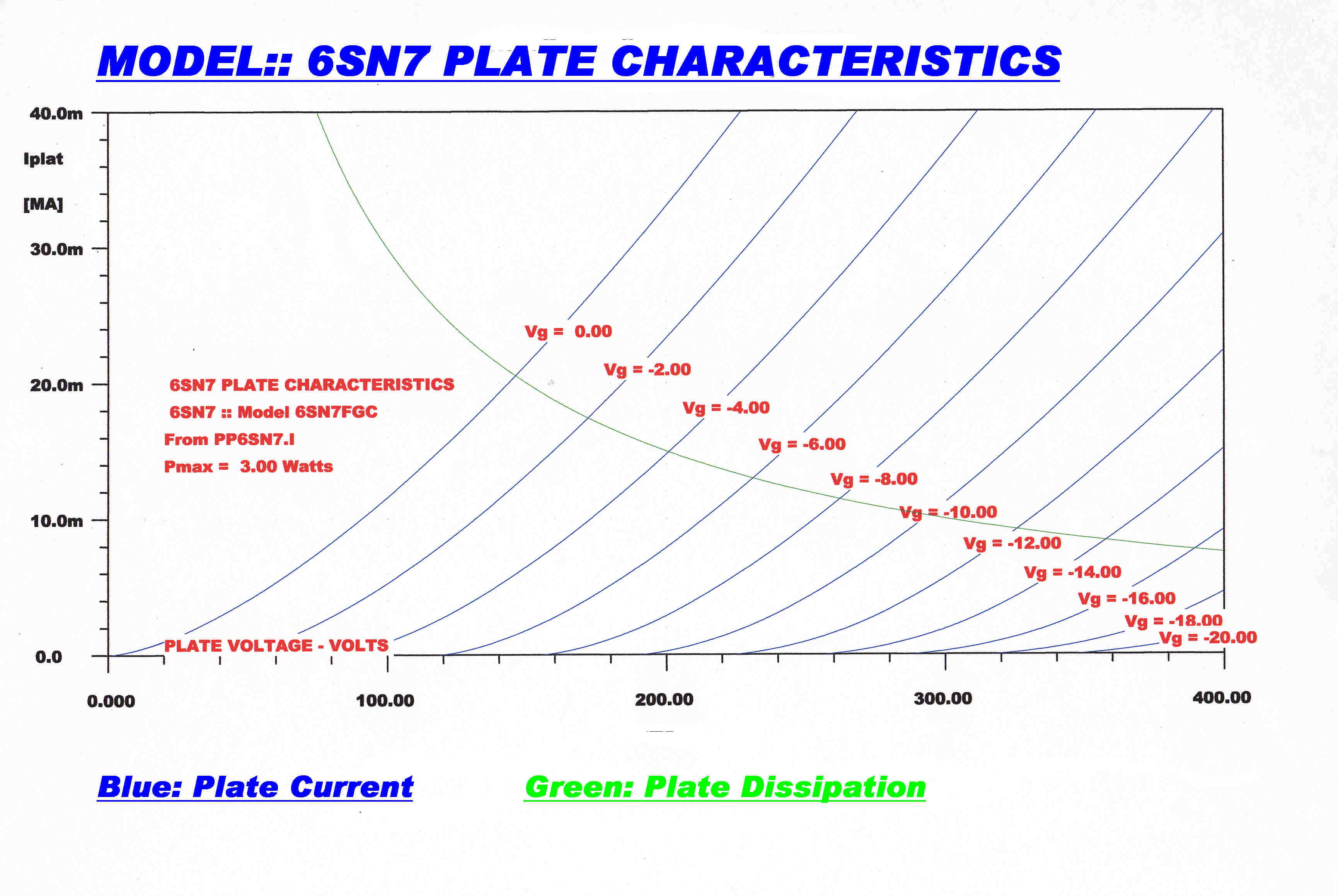
The choice of operating conditions for the 6V6 output pentodes is obvious.
The quiescent current is chosen to bring the plate current up to give the maximum plate
dissipation. This is the maximum dissipation for the tubes since, in class A, the output
power subtracts from the plate dissipation.
The transformer primary impedance is chosen to put a load line through the knee of the plate
current curve to give a good compromise between power output and distortion.
The choice of operating conditions for the 6AC7 and 6SJ7 voltage amplifiers is not so obvious.
The voltage gain A is given by: A = GMRL
GM is grid-plate mutual conductance
RL is load resistance in plate
IP is the quiescent plate current
But RL = VD/IP
where VD is the voltage drop in the plate resistor. This is fixed and equal
to about 1/2 the high tension voltage VBB.
So A = [ GM/IP ] VD
Since VD is fixed, [ GM/IP ] must be maximised.
The plate current control mechanism is space charge limiting, which leads to
the three halves power law:-
Ip = K( VB + vg )3/2
for ( VB + vg ) > 0
GM = dIp/dvg =
(3/2)K2/3Ip1/3
So: GM/Ip = [(3/2)K2/3]/Ip2/3
The attainable voltage gain A therefore increases as the plate current is decreased.
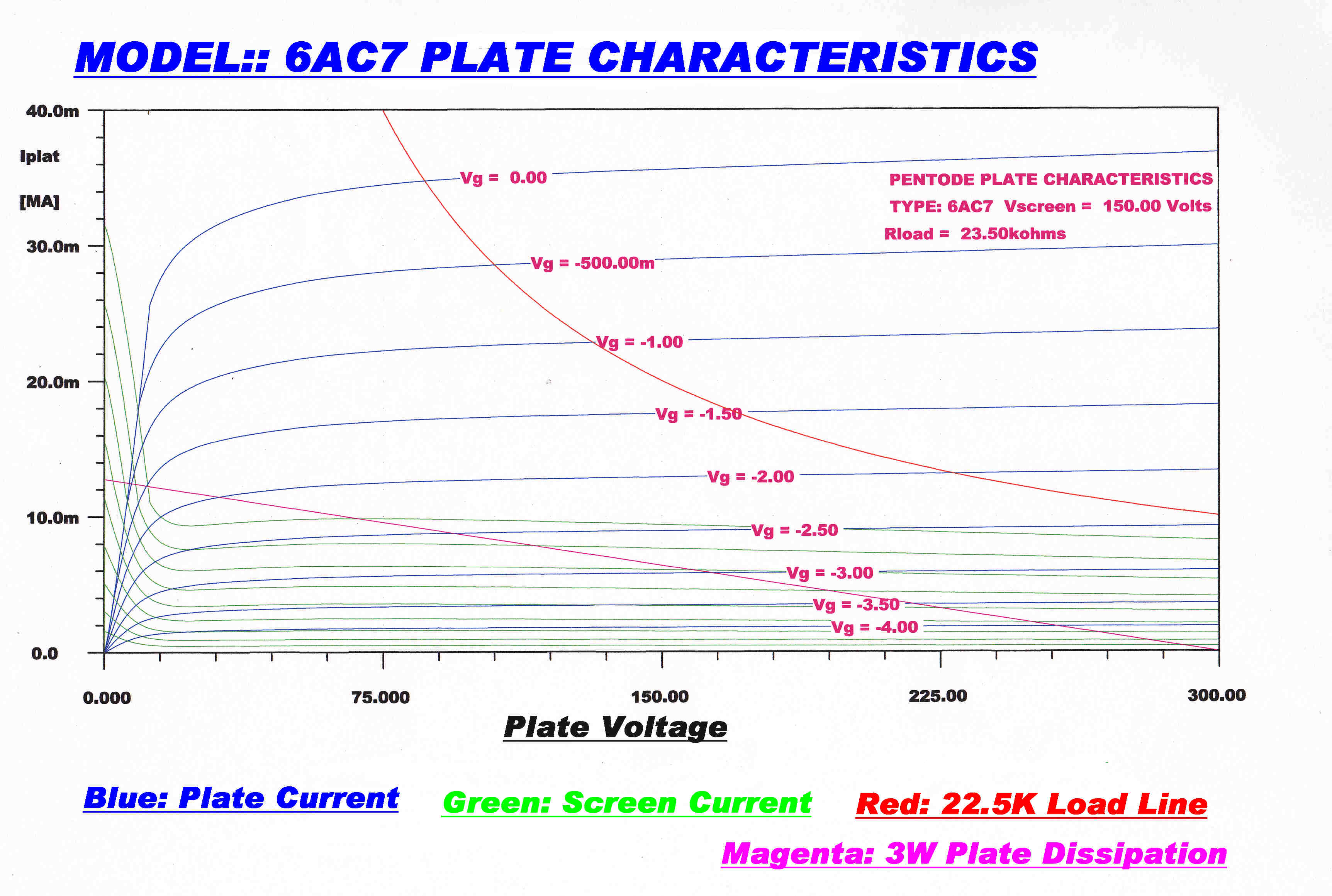
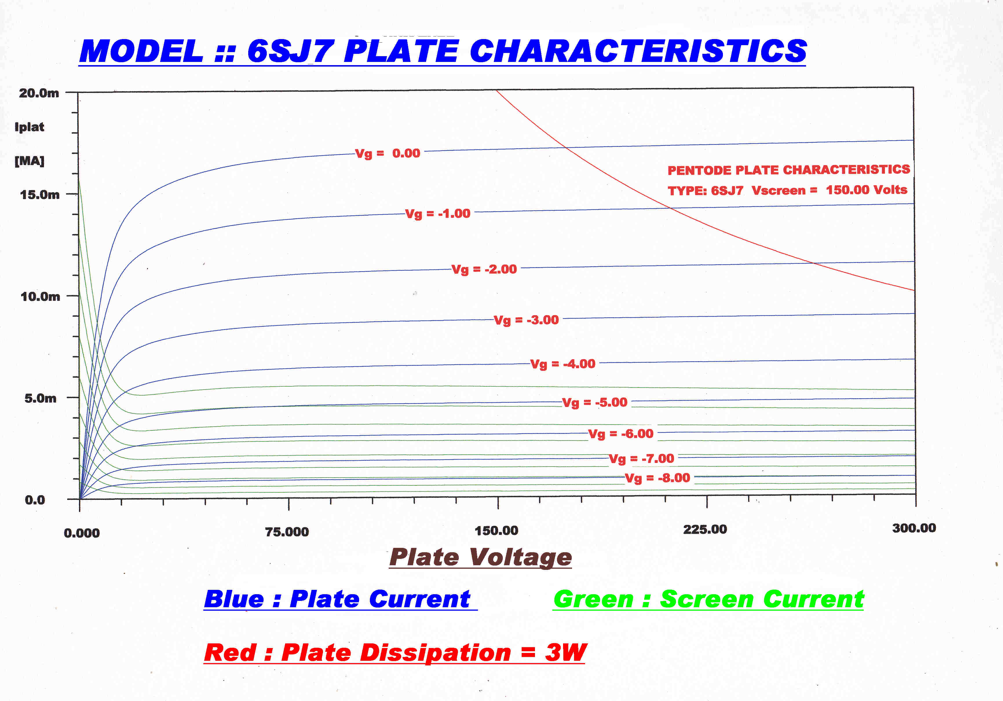
In the early days of vacuum tube amplifiers, tubes like the 6SJ7 were operated with a plate load
of 250Kohms and a plate current of 0.6MA. This optimised the gain and gave a cutoff
frequency of about 30KHz. This was adequate in non-feedback amplifiers.
Here we require a much higher cutoff frequency to give adequate phase margin in the feedback loop at
high frequencies. Gain is sacrificed for dynamic performance, and a much lower plate load of
56K is chosen with a plate current of 2.54MA and a GM = 1.23MA/V
At very low plate currents near cutoff the control mechanism in vacuum tubes changes
from charge control to an energy barrier effect similar to that found in bipolar transistors.
Electrons at the high end of the Maxwellian distribution overcome the energy barrier
of the negative grid to provide a small plate current.
The transfer characteristic of a vacuum tube under these conditions is of the type:-
Ip = Io [ evg/Vref - 1 ]
where Io and Vref are constants.
For working currents, evg/Vref > > 1
So that:- Ip ≈ Io [ evg/Vref ]
Here Gm = dip/dvg = [Io/Vref]
evg/Vref
So Gm/ip = 1/Vref -- a constant.
It turns out that much greater gains can be achieved with this mode than with higher currents
in the three halves power law mode.
Plate loads of 22 Megohms are typical. This gives a cutoff frequency of the order of 800Hz :
useful for DC coupled instrumentation amplifiers, but not for audio work.
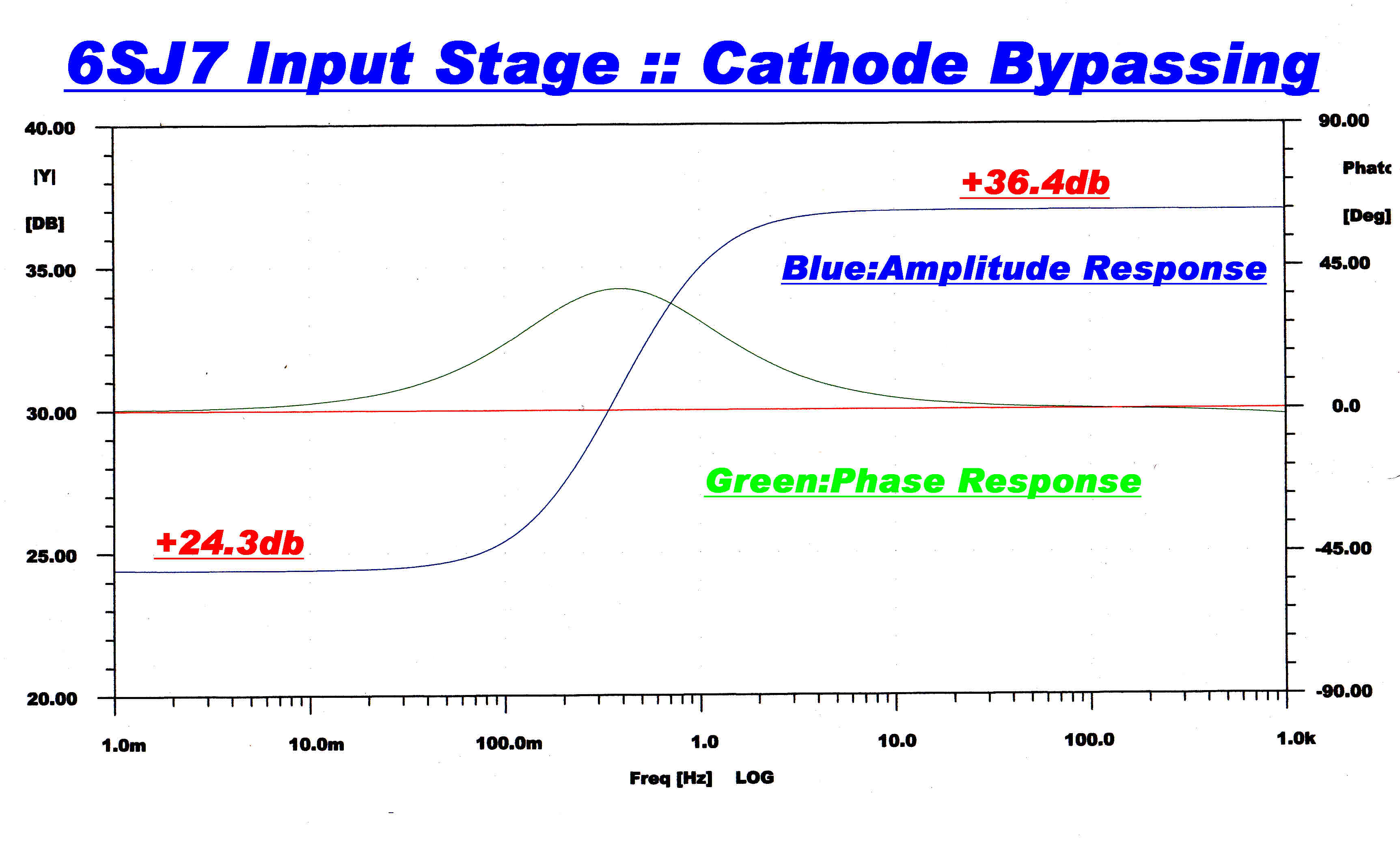
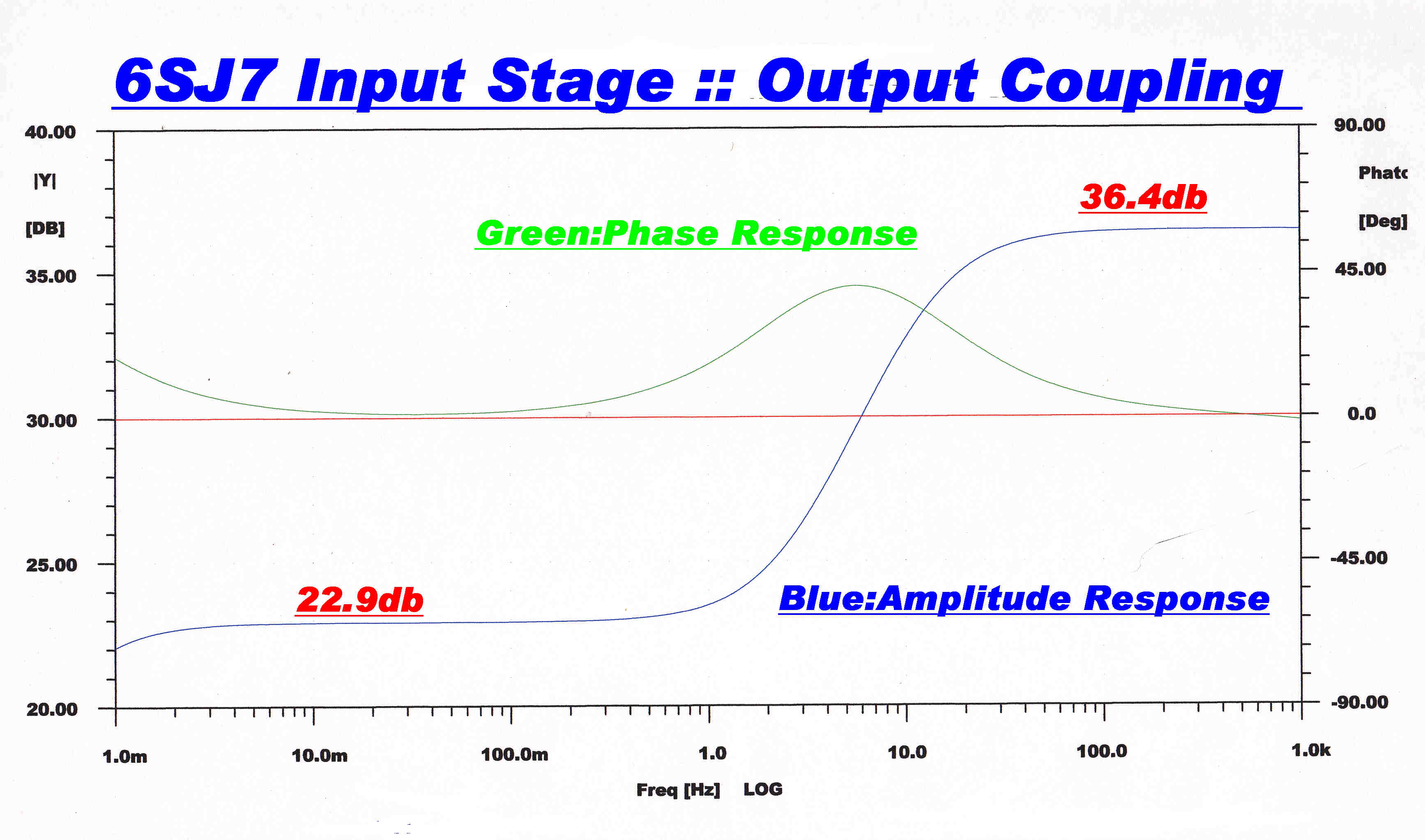
CATHODE BYPASSING of INPUT STAGES
Because of the relatively low gain of the 6SJ7 with a 56K load, the loss of gain
with an unbypassed cathode resistor is not tolerable.
The feedback provided by an unbypassed resistor does reduce distortion in the
stage, but this is of little consequence here, for the output voltage swing, and hence
the distortion, is low.
There is a further advantage in bypassing the cathode resistor. 50Hz current is
injected into the cathode from the heater via capacity and leakage causing hum.
Bypassing the cathode shorts these to earth.
In very low level stages this bypassing is mandatory. Here, in this medium level stage,
it is simply desirable.
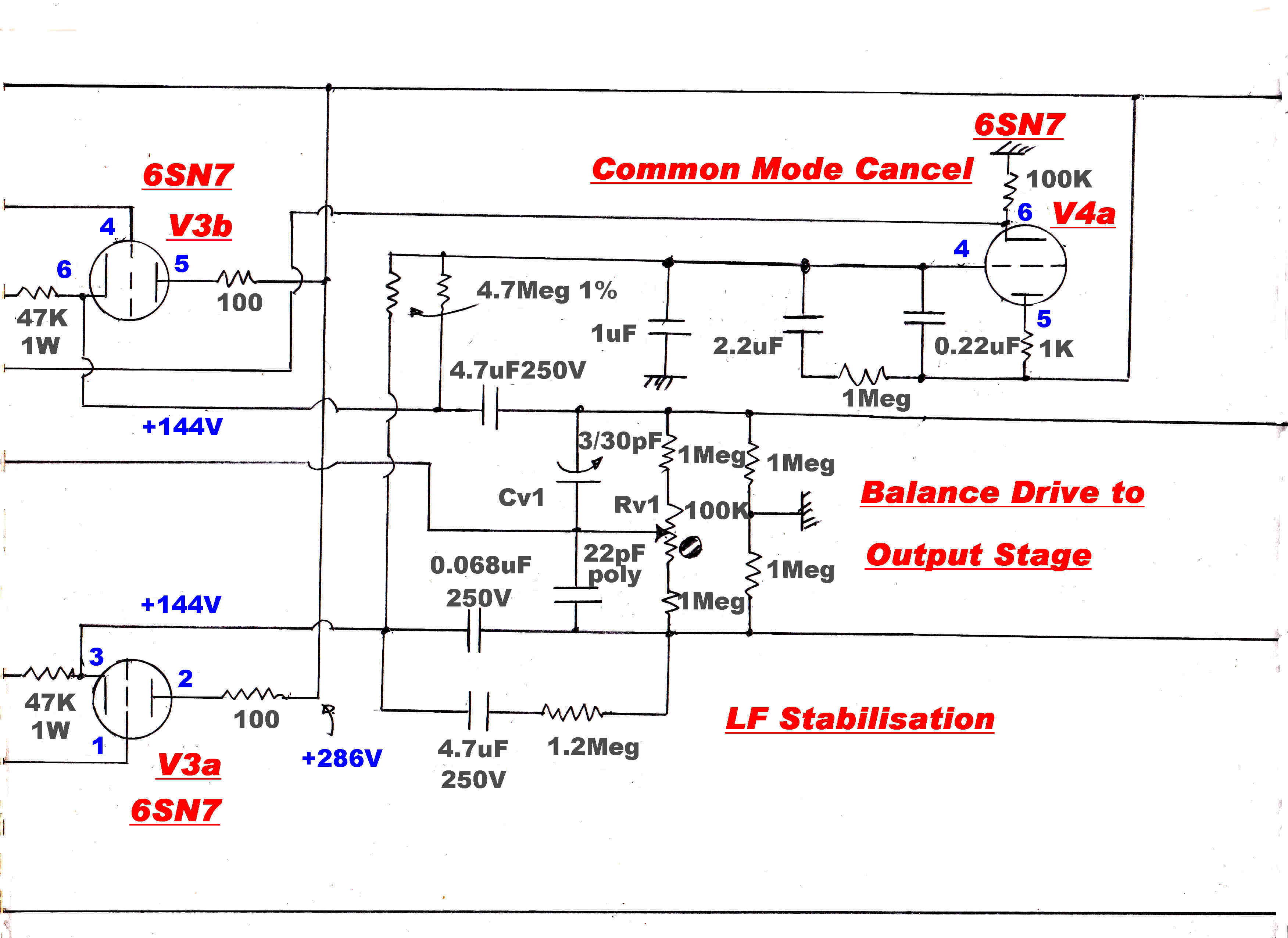
INPUT AND PHASE SPLITTER :: DESCRIPTION
The input stage VT1f is a normal R-C coupled pentode stage with cathode bypassing.
The separate cathode bias resistors on the input and phase splitter stages help stabilise
the tube operating point.
The input and overall feedback signals are combined in the network R1f,R2f,C1f,C2f,
and the error signal applied to the grid of VT1f. The usual practice of driving the grid
with the input and subtracting the feedback in the cathode is dependent on the parameters
of the tube, and so is not as desirable as the technique used here.
The plate voltages of VT1f and VT2f are added in the resistors R16f,R17f. These resistors,
together with C15f,C14f and C30f, form a slow speed low pass filter. The average DC plate
voltage is fed back via the cathode follower VT5f to the pentode screens. This further stabilises
the operating point of the input tubes. Note that push-pull signals cancel and produce
no feedback, so there is no degeneration for push-pull signals.
There is no compensation for tube drift in opposite directions.
The mid-frequency gain of the stage Amf is given by:-
Amf = Gm-gpRL = 1.23x10-3x56x103
≈ 69.
Modification of the forward transfer function for the main feedback loop takes
place in the input stage.
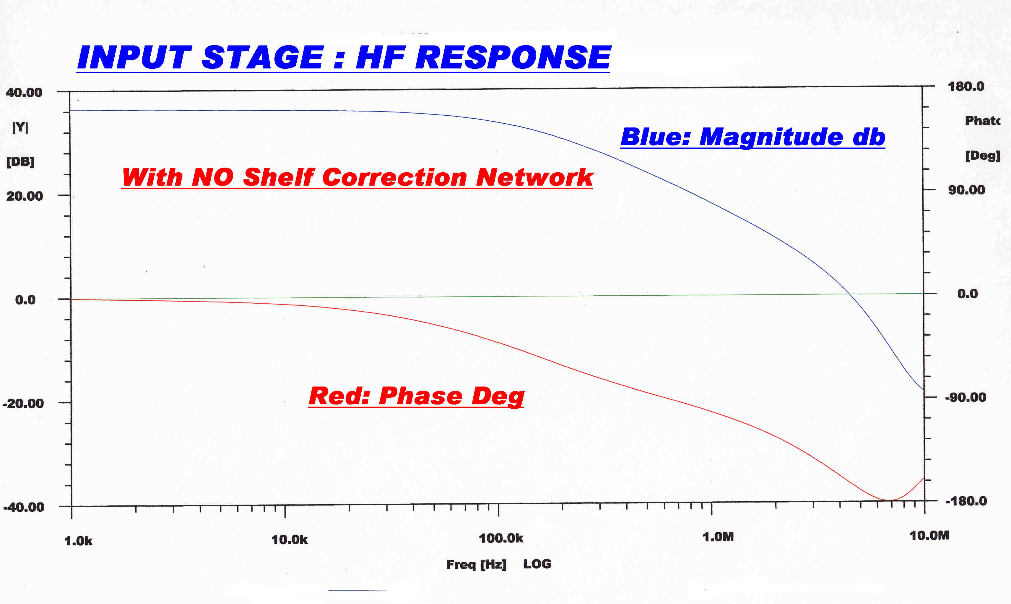
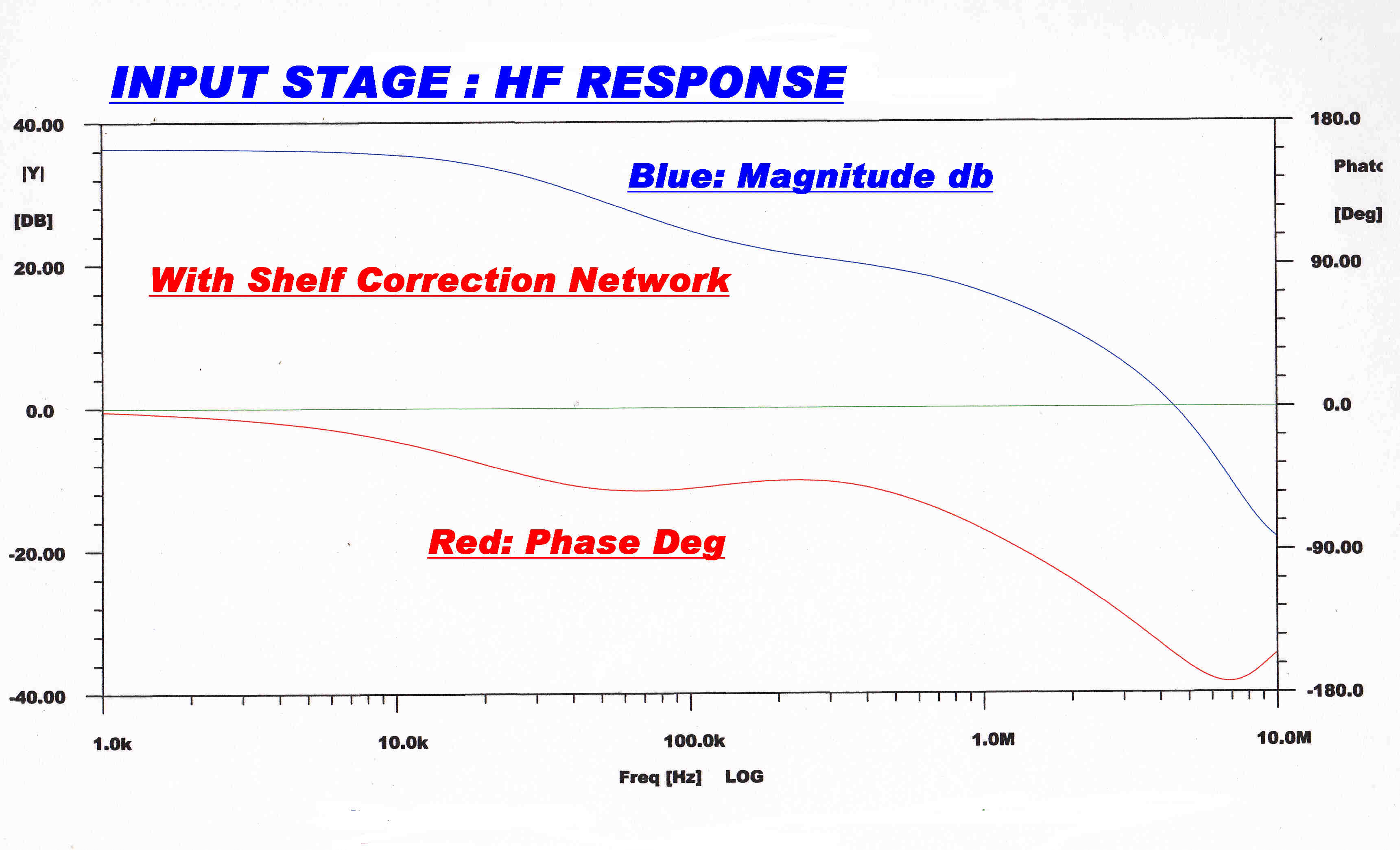
R9f-C6f provide a shelf in the high frequency response.
C8f, C40f, R40f and R20f tailor the low
frequency response of the main loop. This will be described in more detail later.
The phase splitter VY2f, VT4f is an operational amplifier with a loop gain
Aloop given by:-
Aloop = Acfx Ard xAmf where:-
Cahode follower gain Acf ≈ 0.95
Resistive Divider Gain Ard ≈ 0.5
Aloop ≈ 0.95x 0.5 x 69 = 33
The output impedance looking down into the plate is given by:-
Rout = 1/[ Gm g-p Aloop ]
= 1/[ 1.23x10-3 x 33 ] = 24.6ohms
This forms a voltage divider with the 56K load resistor so that voltage transients
on the HT line are suppressed in the phase splitter. Any variation on the plate of
VT1f is inverted and appears on the plate of VT2f.
The input amplifier/phase splitter converts high tension transients to push-pull
signals and suppresses common mode.
The high tension rail is unregulated and responds to slow speed mains transients.
It is desirable to remove them from the push-pull output as well as the common mode output.
The feed-forward suppression technique described above operates on VT1f,
and so removes them from the push-pull output.
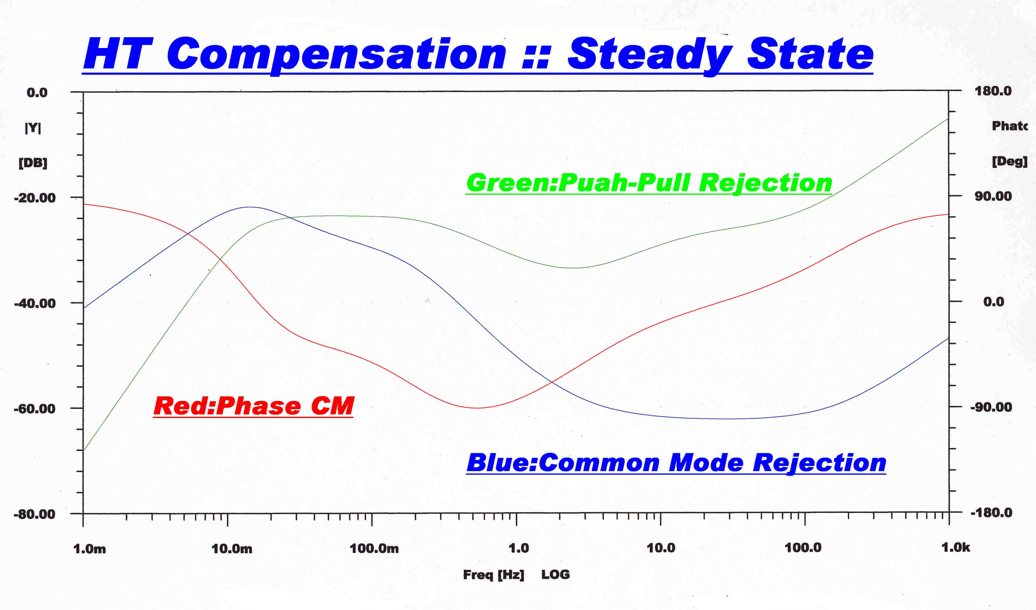 The computer solution for the common mode and push-pull rejection of high tension
transients is shown opposite.
The computer solution for the common mode and push-pull rejection of high tension
transients is shown opposite.
OVERALL FEEDBACK LOOP STABILISATION
GENERAL
The overall feedback loop has the following functions:-
(1) To reduce the output impedance.
(2) To reduce the distortion at low frequencies due to non-sinusoidal
transformer magnetising current.
(3) The distortion in the output stages and phase splitter is low because of internal feedback
with a high return difference.
The distortion in the input stage VT1f is low because its peak output at full power is
+(-) 6 volts. This distortion is further reduced by the overall feedback.
The forward gain in the main feedback loop is 5.34 (14.5db).
It is designed to be fully active between 20Hz. and 30KHz.
If we imagine a 1 volt voltage generator applied to the 4 ohm output, we can calculate the
current swing in the output terminals due to the feedback loop, and so the output impedance.
Zout = 1/ΔIout = 1/[ AR A1 Gm
(Rp / Rs)1/2 ]
where: AR is the attenuation in the resistive feedback network.
A1 is the gain of the input stage.
Gm is the transconductance of the output current loop stage.
Rp is the p-p primary load resistance: Rs is the secondary load.
AR = 2.716x10⁻² : A1 = 69 : Gm = 24.83x10⁻³
Rp = 3300 : Rs = 4 ohms
Rout = 0.746 ohms.
HIGH FREQUENCY
A high frequency shelf is provided by: R7f, R9f, and
C6f.
The transfer impedance Zt(p) =
R1 ( 1 + R2C ) / ( 1 + ( R1 + R2 ) C )
so the low frequency break point is given by:-
fl = 1/2 π ( R1 + R2 ) C
and fh = 1/2 π R2 C
Here: R1 = R7f = 56K R2 = R9f = 15k
C = C6f> = 82pF
So: fl = 27.3KHz. and fh = 129.4KHZ.
The magnitude of the shelf is given by:- fh / fl = 4.73 (13.5db)
Note: C6f is drawn on the earthy end of R9f. This is to prevent
the stray capacity from the body of C6f adding to the stray capacity
C5f .
In vacuum tube technology every little pF counts.
The effective load resistance at high frequencies is now R9f||R7f
= 11.83Kohms, so the high frequency cutoff is extended by ( 56/11.83) 4.7.
This improves the stability of the high frequency feedback loop still further.
The overall response of the input/phase splitter is given below.
|
|
|
No Correction Network |
With Correction Network |
LOW FREQUENCY
The AC coupling networks and the primary inductance of the output transformer
can give rise to severe low frequency stability problems in the overall feedback loop.
(1) The inductance, and so the low frequency turnover of the output transformer,
is level dependent.
It is highly desirable that the transformer low frequency transfer function NOT
enter into the active region.
To achieve this, the low frequency loop gain has to fall below unity before
attenuation caused by the transformer primary inductance starts.
Distortion due to non-linear magnetising current is worst at 20HZ, so the
feedback loop should still have its maximum forward gain at this frequency.
This sets the upper limit at which low frequency attenuation in the forward
gain can begin.
The networks that determine the forward loop are:-
(1) The output transformer primary inductance and reflected load.
(2) The current feedback around the output stage.
(3) The stabilistion network providing the AC coupling between the input/phase
splitter and the 6AC7 - 6V6 output stage.
Here (1) and (2) can be considered as fixed or given.
However, the coupling network (3) can be tailored to give
a stable overall open loop transfer function.
The steady state response of the transformer and output stage is shown below.
|
|
|
|
Transfer Impedance of Output Stage with Current Feedback |
Transfer Impedance of Output Transformer with Resistive Load |
We can now develop the low frequency stabilisation strategy.
(1) The transformer and output stage can be considered flat down to about 1 Hz.
(2) The forward gain in the main loop is 5.34.
(3) We can now design a shelf between 10Hz. and 2Hz. in the input amplifier to
reduce the gaim by about 5.
(4) This leaves full feedback oprative at 20Hz., but reduces the loop gain
below 1 before significant phase change occurs in the rest of the loop.
Examination of the steady state transfer function shows that this attenuation
can be extended to lower frequencies without endangering loop stability.
This increases the low frequency gain stability margin still further.
Design of Low Frequency Stabilisation Network
The realisation of the low frequency shelf in the output coupling network will
now be outlined.
 The steady state response in the input amplifier due to the cathode bypass
capacitor C3f (470uF) and R4f (1.8K) is shown
opposite.
The steady state response in the input amplifier due to the cathode bypass
capacitor C3f (470uF) and R4f (1.8K) is shown
opposite.
Its attenuation starts at about 1Hz., but we want this to start at 10Hz.
The coupling capacitor C8f can start the 10Hz. break.
 The steady state response of the coupling network.
This consists of C8f, C40f, R40f
and the total resistance Rtot of the 18f node to earth.
C18f and Rtot produce attenuation at 6db/octave
down to zero Hz.
When the reactance of C8f rises to equal R40f
attenuation ceases and a flank is produced.
This gives the correct transfer function but introduces unwanted DC on
the node 18f. C40f is introduced to block this DC voltage.
It is made large, so its reactance is much smaller than
R40f over the working frequency range of the network.
 The combined response of the coupling network and the cathode bypassing
is shown opposite.
The combined response of the coupling network and the cathode bypassing
is shown opposite.
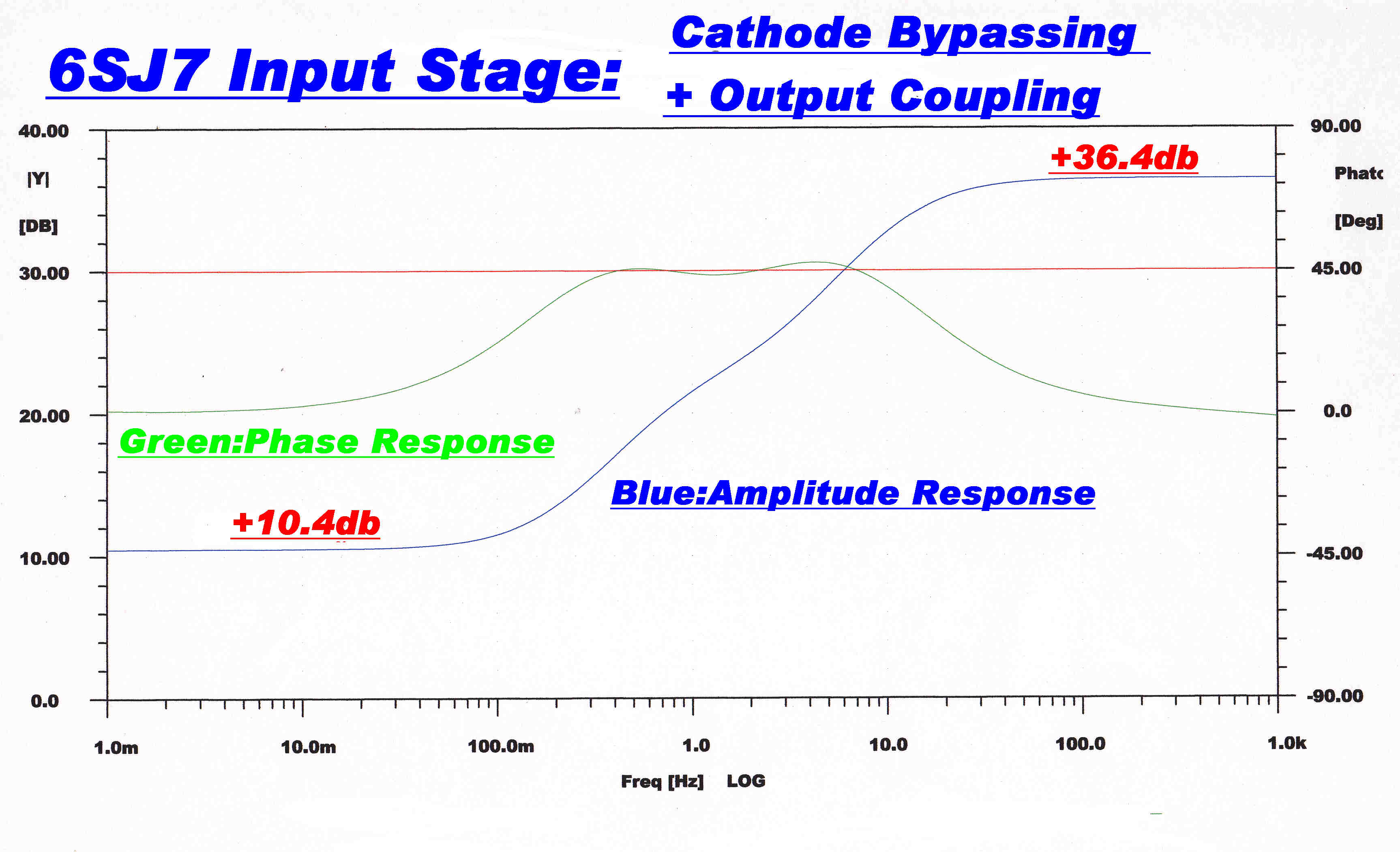
A shelf having a constant phase change of about 45 degrees is formed between
10Hz. and 0.3Hz.
The shelf safely disposes of a large amount of gain ( 36.4 - 10.4 = 26 )db.
26db = attenuation of x 20.
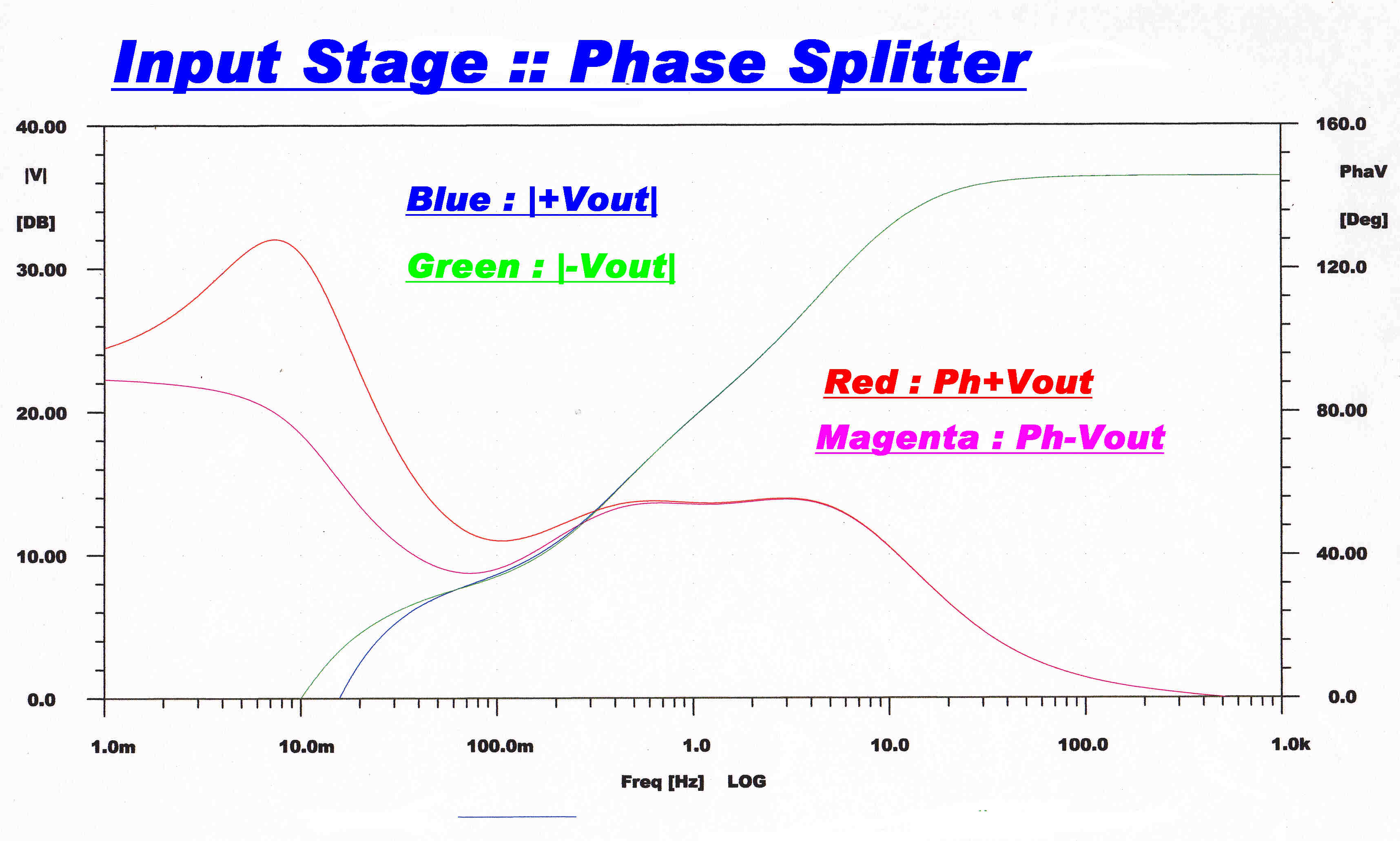 The response for each side of the phase splitter output is plotted.
The gain of each side is matched well below 0.1Hz and the phase change
is the same down to 1 Hz - both below the working frequency of the amplifier.
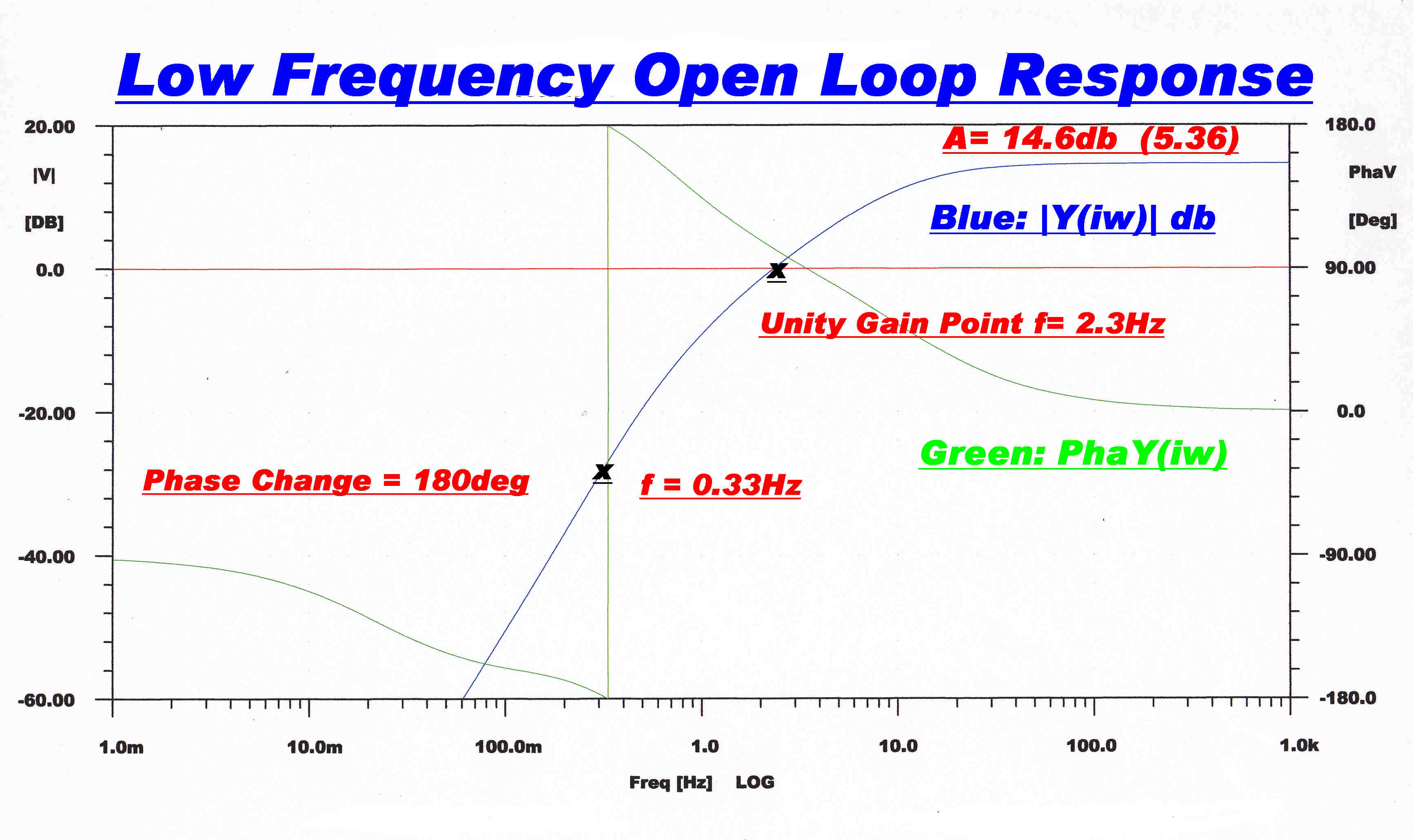 The low frequency open loop response of the complete amplifier is shown opposite.
The unity gain frequency is 2.3Hz.
The frequency for 180 degree phase change is 0.33hz.
This indicates that low frequency loop should be very stable.
Virtually full gain is operative at 20 HZ. to reduce distortion due to
non-sinusoidal magnetising current.
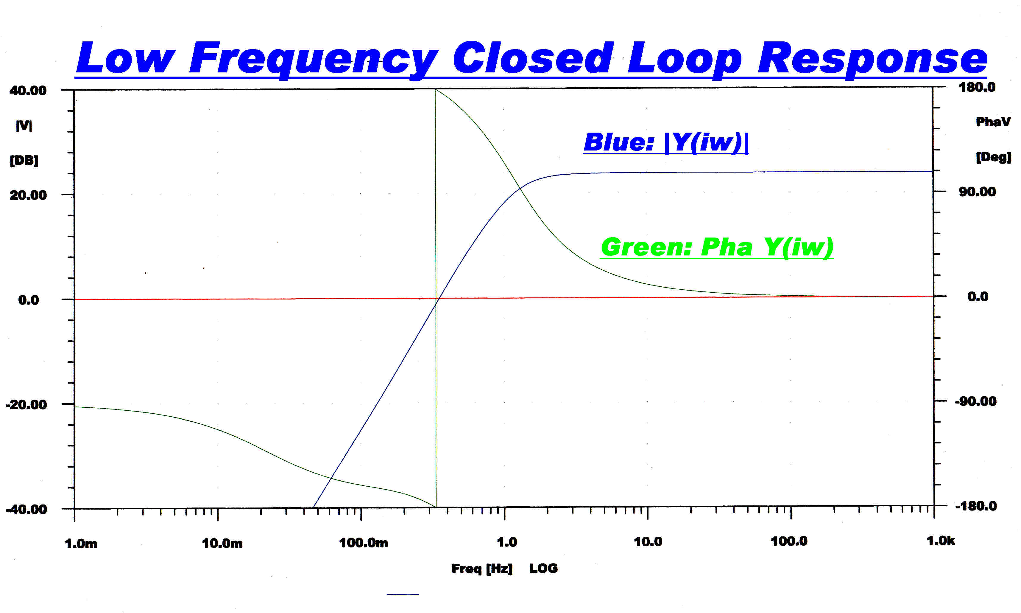
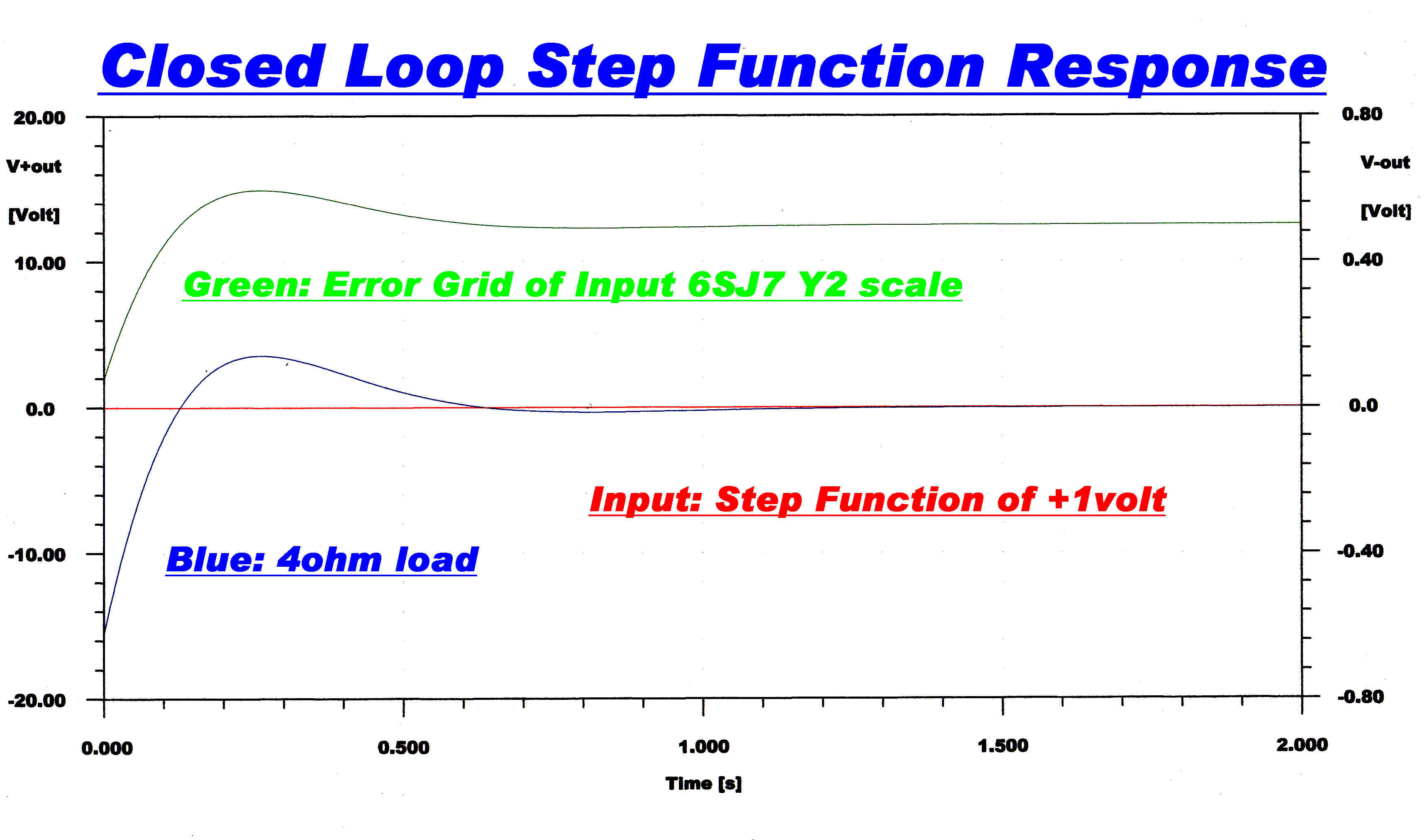
CLOSED LOOP RESPONSE
The closed loop steady state and transient response is shown below:-
|
|
|
The amplitude response does not have a low frequency peak for the
primary inductance of the transformer measured for low level signals. |
The error signal is plotted on the Y2 axis. |
Note that the step function response crosses the axis twice.
A useful rule when designing slow speed transient response is given by:-
Number of axis crossings = [Ultimate Slope/Octave(db)]/6 - 1
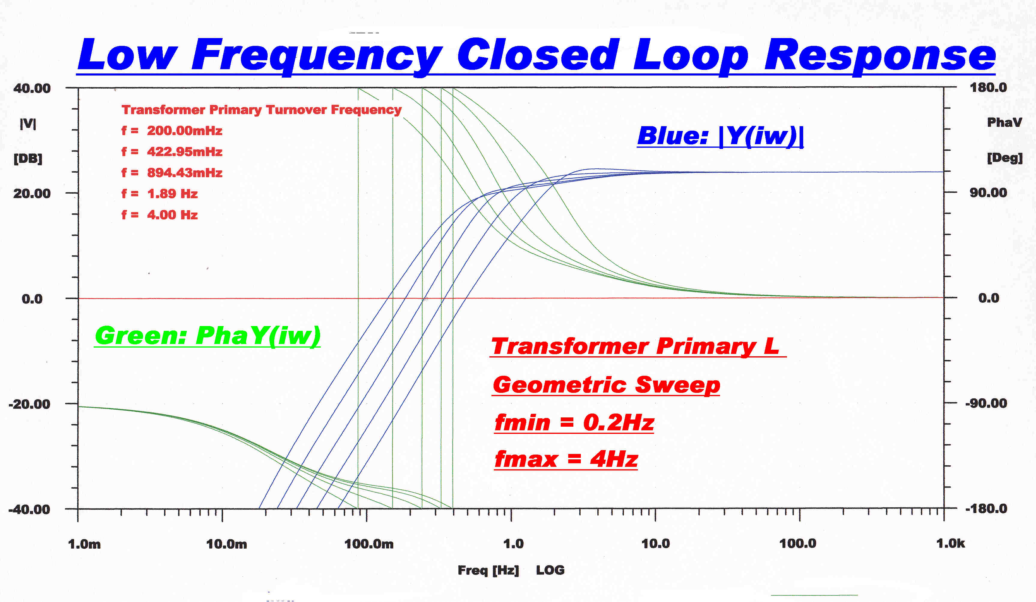 The transformer primary inductance is level dependent.
It s prudent to explore the sensitivity of the overall closed loop response
to the corresponding variation in turnover frequency.
Shown opposite is computer run for a geometric variation in turnover frequency
from 0.2 Hz. to 4 Hz.
Small variations in the response are insignificant and well below the operating
frequency range of the amplifier.
|
|
|
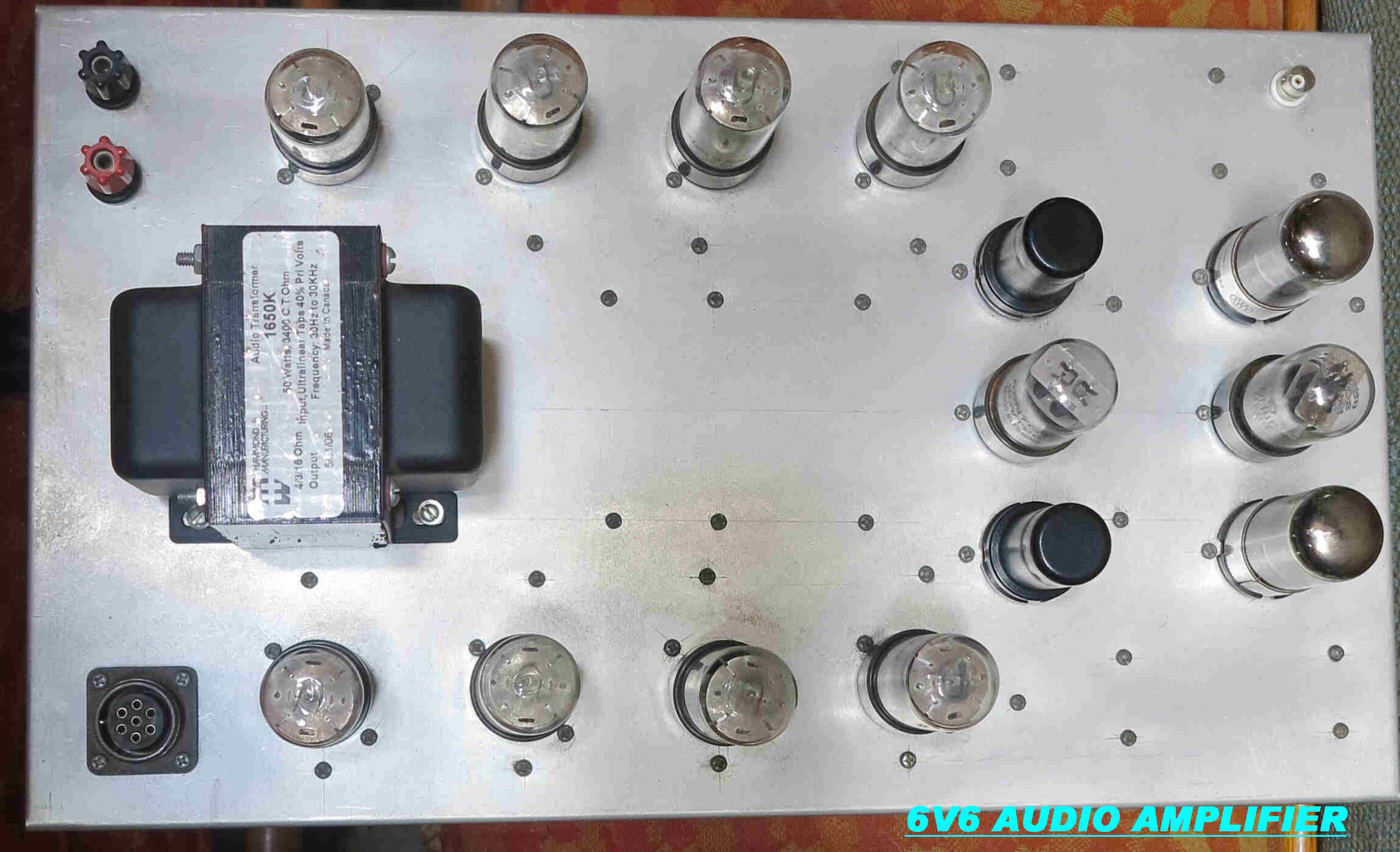
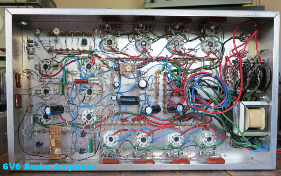
The symmetry of the push-pull design is reflected in the layout. |
Point to point wiring is used. |
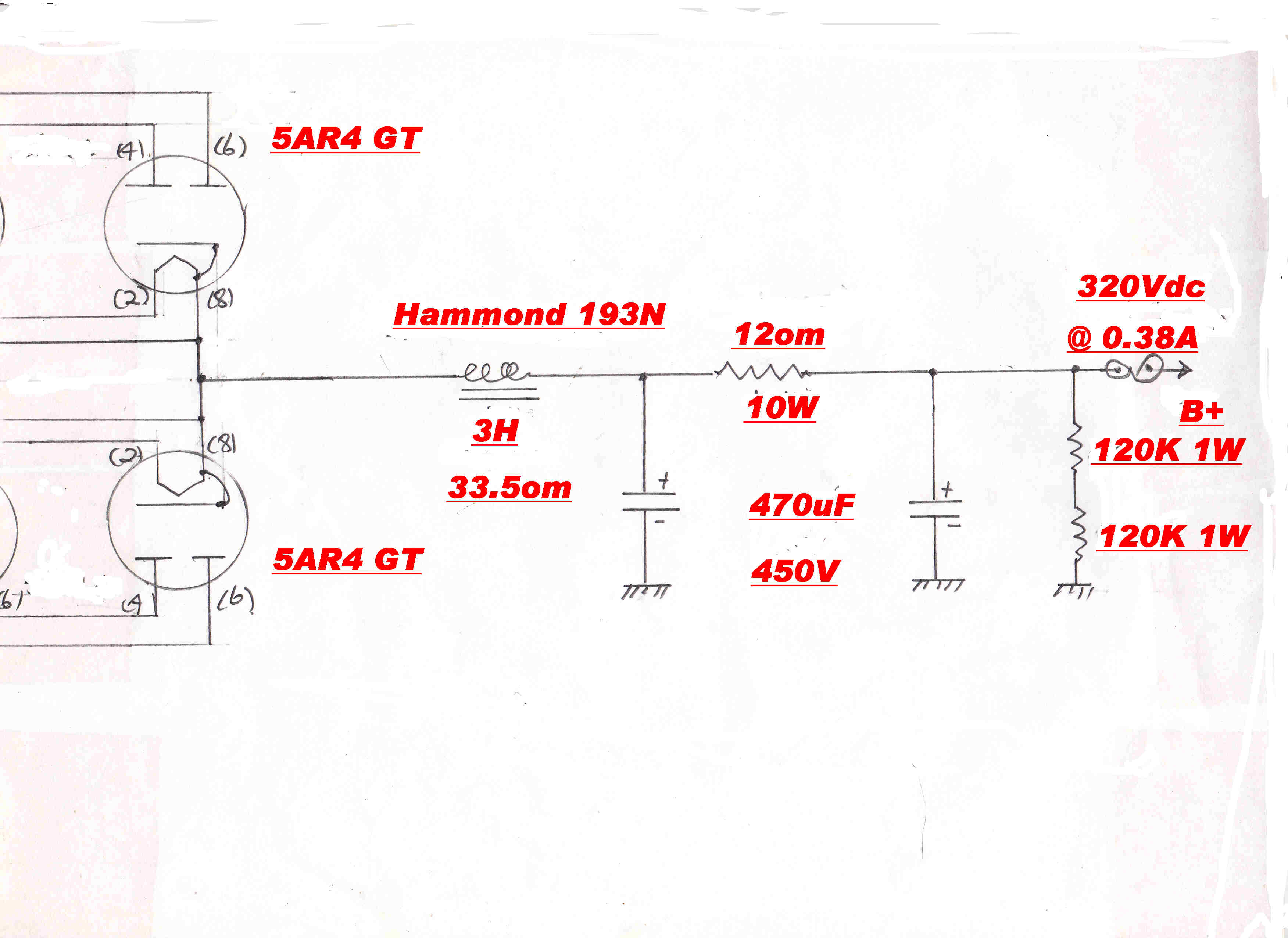
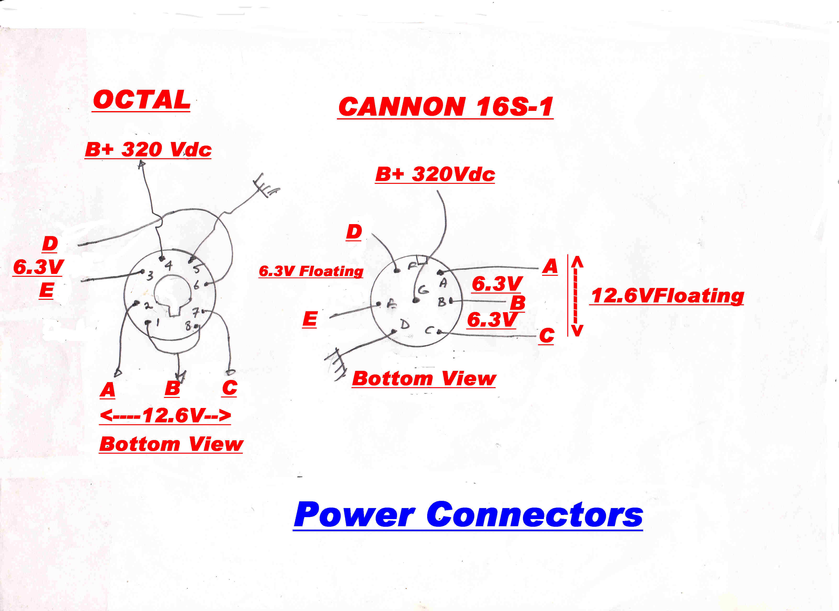
The circuit of the power supply for the vacuum tube amplifier is shown below.

|
|
|
BASIC DESIGN
A class A push-pull amplifier presents a constant load to the power supply.
Because of the three halves power law, there is usually a small increase in current as
the output from the amplifier increases.
The heavy current feedback, together with the unbypassed cathode resistor, in the output stage
greatly reduces this increase, so the load is practically constant regardless of power output.
Output voltage Vo = 320 volts: Load current IL = 0.38 amps:
RL = Vo / IL = 320/0.38 = 842ohms.
FILTER
A choke input filter (with sufficient inductance) produces rectangular
current pulses of half cycle duration in the rectifiers.
A capacity input filter produces short current pulses of high peak current.
Since the RMS value of the rectangular pulses is much less than that of the short high current
pulses, a choke input filter results in much less dissipation in the rectifiers
and transformers.
It is therefore highly desirable and greatly extends the life of the
rectifiers and transformers.
The capacity input filter gives a higher output voltage and lower ripple,
and so finds a place in non-profrssional gear.
CRITICAL INDUCTANCE
A minimum value of inductance called the critical inductance is required
to prevent the rectifier from acting as a capacity input rectifier.
This inductance LC is given by:-
LC = RL/[ 6 Π f ]
Here RL = 842: f = 50 : so LC = 0.894H
Choose 3 H -- well above the critical value.
OUTPUT RIPPLE
When the inductance is above critical, the output waveform from
the rectifier is a full wave rectified sinusoid.
This can be expanded out in a Fourier series to give:-
v(t) = Vp[ 2/Π - 4/Π ∑ (cos( k ω t ))/( k + 1 )( k - 1 ) ]
for k even: k ≠ 0
Because the ultimate slope of the L-C-R filter is 18db/octave, the only significant
frequency in the output ripple is 100Hz.
The L and C components in the filter of a power supply usually have a fairly high
tolerance, so approximate calculations for output ripple are appropriate.
For instance, the inductance is quoted as 3H with a DC current of 500Ma. At 380Ma the
inductance is probably higher and furthermore non-linear.
Secondary Output Voltage Vrms = 375V
So Vp = √2 Vrms : Vp = 530V
From the expansion above with k = 2, K = 4/[3 Π ]
where K = Vsec/Vfund = 0.4244
The peak value of the second harmonic on the cathodes of the rectifier Vsec
is then given by:-
Vsec = 530 x 0.4244 = 225 volts
When the capacity C forms a simple voltage divider with the inductance of the choke L.
The attenuation A is given by:-
A = [ 1/i ω C ] / [ 1/i ω C + i ω L ]
Then A = 1/[ 1 - ω2 L C ]
The reactance of the first 470uF filter capacitor is 3.39 ohms at 100Hz, so the filter can be approximated
by two independent sections:-
[1] an L-C filter of 3H and a capacitor of 470uF
[2] an R-C section with R= 12 ohms and C = 470uF
For the first section the attenuation A1 = 1.8 x 10⁻³
so the output ripple is approximately
225 x 1.8 x 10-3 = 0.4V peak
For the second filter the attenuation A2 is approximately
A2 = 3.39/12 = 0.283
The peak output ripple is then 0.283 x 0.4 = 0.11V
For the L-C filter for the low level stages in the amplifier: L = 15H: C = 22uF
So A = 7.735 x 10⁻³
And the output ripple is approximately 0.11 x 7.735 x 10-3 = 0.9mV
CHOICE of THERMIONIC RECTIFIER
A diode with an indirectly heated cathode (5AR4-GT) is much more desirable than
those ( 5Y3, 5Z4, 5AU4, 5AS4 ) with filamentary cathodes.
(1) The dimensions are under tighter control, so the tubes can be manufactuured with
smaller plate cathode spacing giving a lower voltage drop.
For 100Ma plate current the tube voltage drops are:-
5AR4 .... 10V
5Y3 .... 43V
5AS4 / 5U4 .... 26V
5Z4 .... 17.4V
(2) The thermal time constant of a filamentary cathode is much less than that
of an indirectly heated cathode. This means that the B+ high tension rail comes
up to full voltage before emission begins in the amplifier tubes.
Since the load presented by the amplifier is very high, the inductance is
below critical, and so the high tension reaches the peak output voltage from
the secondary of the transformer. (530V)
Further, a significant fraction of this starting transient is applied to
the grids of the amplifier tube via the load resistors and coupling capacitors.
This produces an intense electric field at the surface of the cathode
as emission starts.
It is claimed that this reduces the life of the cathode.
With modern frame grid tubes such as the ECC88/6DJ8 the field is sufficient to cause
break down ( probably due to field emission) and the tube is destroyed.
To prevent this small neon tubes are placed between the grid and cathode.
In this amplifier all the tubes were available by 1938 and the grid cathode
spacing is large enough to prevent initial failure, but perhaps the addition of
neon tubes is still a good idea.

|
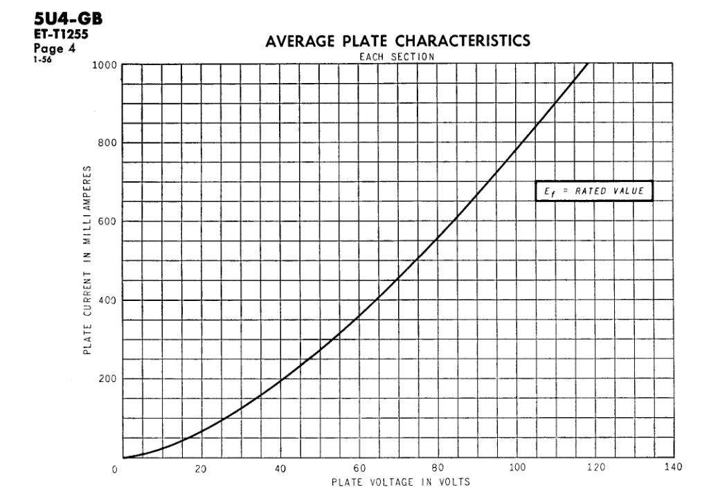
|
|
5AR4 PLATE CHARACTERISTICS |
5AS4 PLATE CHARACTERISTIC |
HOT SWITCHING
The momentary disconnection of mains voltage from a power supply can lead to
dangerous conditions.
The thermal time constant in the cathode maintains emission during the transient.
In a capacity input rectifier full mains voltage is suddenly applied to the capacitor.
The switching transient can be large and destructive, and is limited only by the output
impedance of the transformer and the rectifier voltage drop.
A choke input filter greatly reduces the peak value of hot switching transients.
FILAMENT SUPPLY
The main filament supply is arranged so that it is effectively 12.6 volts
rather than 6.3 volts. This reduces voltage drop in the connecting lead.
The filament supply is earthed only at the amplifier to prevent circulating currents and hum.
Two cathode followers in the amplifier have their cathodes raised to about 150 volts DC.
A floating filament supply is raised to this DC level to minimise the cathode to filament
voltage. Most run of the mill tubes of 1938 vintage can operate with a cathode - filament
potential difference of 150 volts, but it is good practice to reduce it.
TURN OFF TRANSIENT
Standing currents in inductors produce transients at turn off.
[A] Turn off may occur when the magnetising current in the transformer primary is at a maximum.
This can cause very high reverse voltage transients across one rectifier tube
in choke input filters, but not in capacity input filters.
[B] The transient caused by the full load current flowing in the filter inductor does not produce
large reverse voltages on the rectifier.
[A] An estimate of the order of magnitude of the transient due to switching
the magnetising current at its peak follows:-
Magnetic energy in the transformer core Em = 1/2 L I2
This is then dumped into the stray capacity across the primary C.
The energy stored in the capacity C across the winding Ee = 1/2 C V2
where I is the peak value of the magnetising current: V is the peak volltage transient
across the winding.
So Em = Ee
1/2 L I2 = 1/2 C V2
V = [ L/C]1/2 I
For the two transformers in parallel approximaate values are:-
L = 5.88H: C = 1nF: I = 0.255A so that the peak voltage across the primary Vpriis:-
Vpri = 19.6KV
This causes a peak voltage of Vpk across both ends of the secondaries where :
Vpk = (2 x 375)/240 x Vpri = 61KV!
The conducting diode pulls its cathode to the peak positive potential at one end of the secondary
and this full reverse voltage appears across the non conducting diode, since the filter inductor
can have little effect at the high ringing frequency fo = 20 8 KHz.
The addition of a 2uF capacitor across the primary reduces the peak value of the transient voltage
Vpri to a safe value.
Here L = 5.88H: C = 2uF: I = 0.255A so that Vpri = 437 volts.
In a capacity input rectifier, all the primary magnetic energy is dumped into the first capacitor.
Because of its size, the capacitor voltage rises very little from its DC value Vo, say, 300
volts and clamps the voltage across the transformer.
The change in capacitor voltage Δ V is given by:-
ΔV = [1/2][ L/CVo][ I^2]
If C = 350uF and Vo = 300 V , Δ V = 1.8 volts.
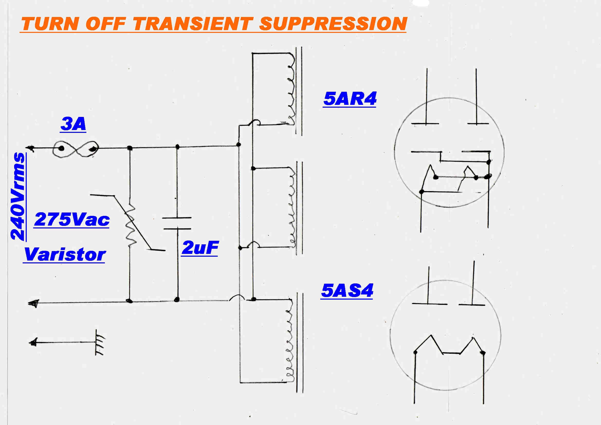 Modifications to the power supply to suppress transients are shown opposite.
On turn off the peak magntising current is diverted into the 2uF capacitor to produce a peak
voltage of 437 volts and a ringing frequency of 464 Hz.
A mains voltage varistor is added for further protection from mains transients.
The detailed internal connections of the 5AR4 and and 5AS4/5U4 rectifier double diodes is also shown.
SUBSTITUTION OF THE 5AS4 FOR THE 5AR4
The 5AS4 may be plugged directly into an octal socket wired for the 5AR4.
This results in a small reduction of the B+ 320 volt high tension rail with a ccorresponding reduction of
peak power output.
The AC filament voltage in the 5ASR will either add or subtract from the AC plate voltage depending on the
random phasing of the transformer connection.
The filament connected to pin2 has more disturbing voltage than the side connected to the output pin, pin 8.
This causes some unbalance in the two diodes.
In amplifiers designed specifically for the 5AS4 diode balance is achieved by taking the output from a centre tap
on the 5 volt filament winding.
The peak current through each diode is about 120MA. , so the voltage drop in the 5AS4 is sbout 28
volts, and this tends to mitigate against the unbalance due to the small filament voltage.
The voltage drop across the 5AR4 is about 11 volts.
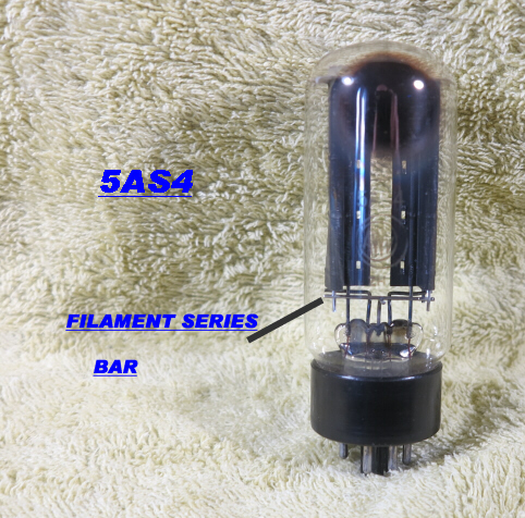
|
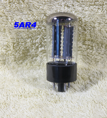
|
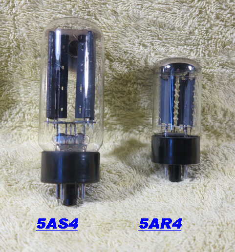
|
|
A bar connects the two filament cathodes of the 5AS4 in series. |
The heaters and unipotential cathodes of the 5AR4 are connected in parallel. |
The relative size of the 5AS4 and 5AR4. |
Photos of tubes in production by 1940 are shown below.
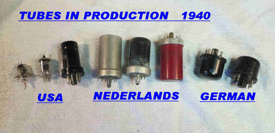
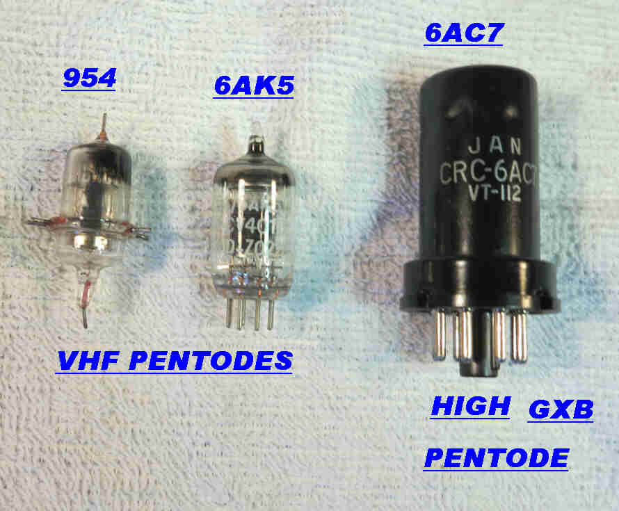 Three US tubes of advanced design in 1940 are shown opposite.
The 954 and 6AK5 are VHF pentodes suitable for the front end of receivers in 200MHz radars.
The 6AC7 is a steel high gain- bandwidth tube employed in the 30MHz IF and video stages of radar and television.
PPI radars rquired a high bandwith with high gain and frequently employed from 8 to 10 6AC7s in the 30MHz IF.
Operation at 200MHz required a very small electrode structure and very short leads.
The leads in the 954 acorn pentode were reduced by a special base structure.
The construction of the 6AK5 was more conventional.
Details of the design and construction of acorn tubes like the 954 are given in:-
RECENT DEVELOPMENTS IN MINIATURE TUBES
by Bernard Salzberg and D.G. Burnside
Proc. IRE October 1935.
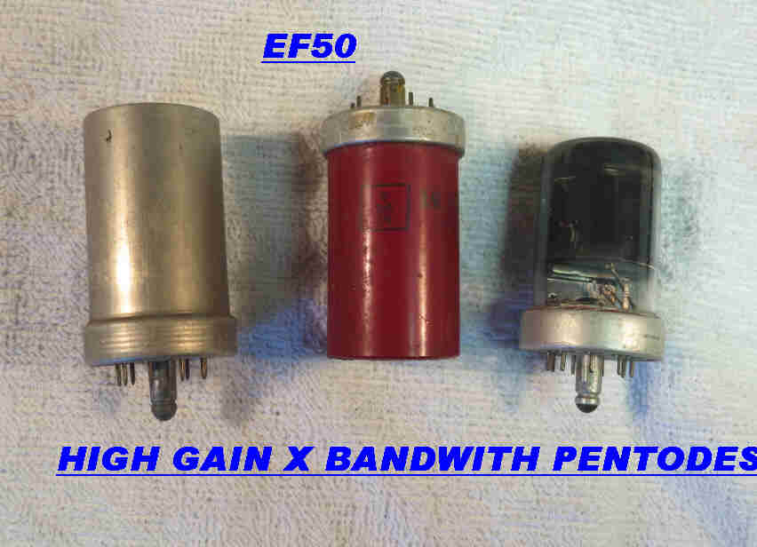 Three EF50s - a high gain - bandwidth tube designed by Philips of Holland in the late
thirties are shown opposite.
Three EF50s - a high gain - bandwidth tube designed by Philips of Holland in the late
thirties are shown opposite.
The tube has a metal shield but is a glass tube. The only tubes with a metal envelope appear to be the 6AC7 of the USA
and the EF14 of Germany. They required special and difficult techniques in their manufacture.
By the mid thirties it became obvious that the pinch construction of tubes led to long leads and high input capacities -
limiting the gain bandwidth products necessary for television and radar.
The EF50 introduced a new base with short leads and plate - grid shielding.
Details of the design and construction of the EF50 are given in:-
A NEW PRINCIPLE OF CONSTRUCTION OF RADIO VALVES
Philips Technical Review June 1939
A NEW ALL GLASS VALVE CONSTRUCTION
by F Prakke, L.H. Jonker, J.O. Strutt
Wireless Engineer 1939.
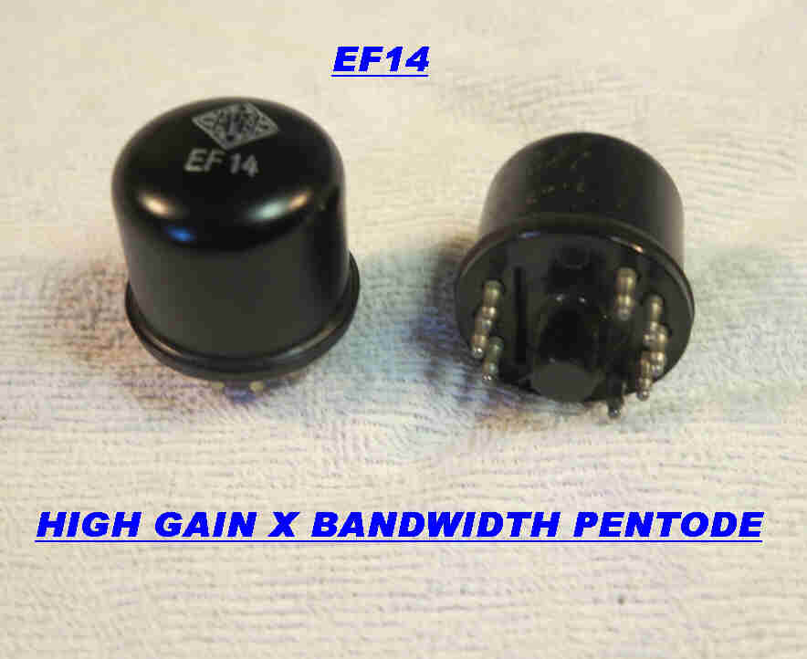 Two EF14s -- the German version of the high gain - bandwidth tube.
The tube had a metal envelope and differed from all other tubes:-
[A] The electrodes were parallel to the base rather than at right angles as in the 6AC7 and the EF50.
This allowed better separation of the plate and grid leads.
[B] The pins were not uniformly distributed, but were asymmetric in two groups of 5 and 3 making
miss - registration impossible. Registration in the 6AC7 and EF50 was produced by a ridge in the centering pin..
[C] The pins were sloped to give a positive capture by the octal socket. This was particularly appropriate
for military use.
The EF14 was used in both IF strips and the video sections of the Wurzburg tracking radar
( the receiver was a double conversion receiver) and in the video amplifier sections.
It was also used in the IF and video sections of the Einheitsfernseher E1 television receiver.
Both are outstanding examples of design techniques of the late thirties.
Drawings of the internal structure of the EF14 are shown below.
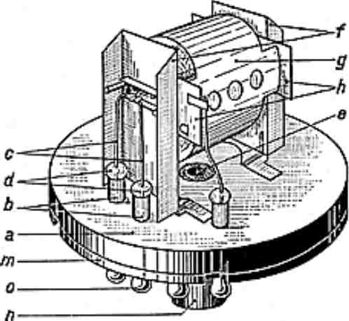
|
|
|
|
Grid - Cathode Side |
Plate - Screen Side |
Mid View |
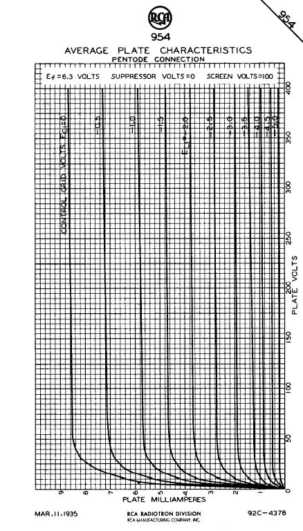
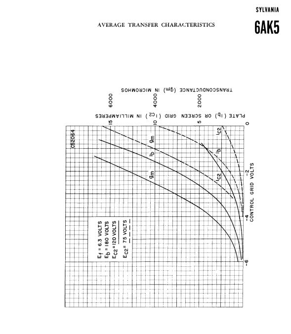
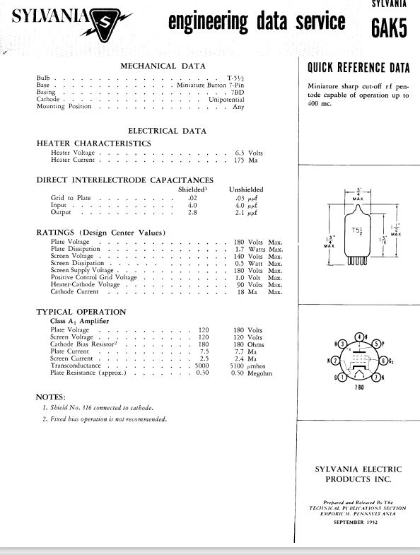
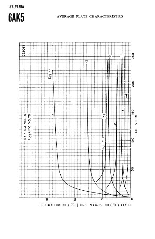
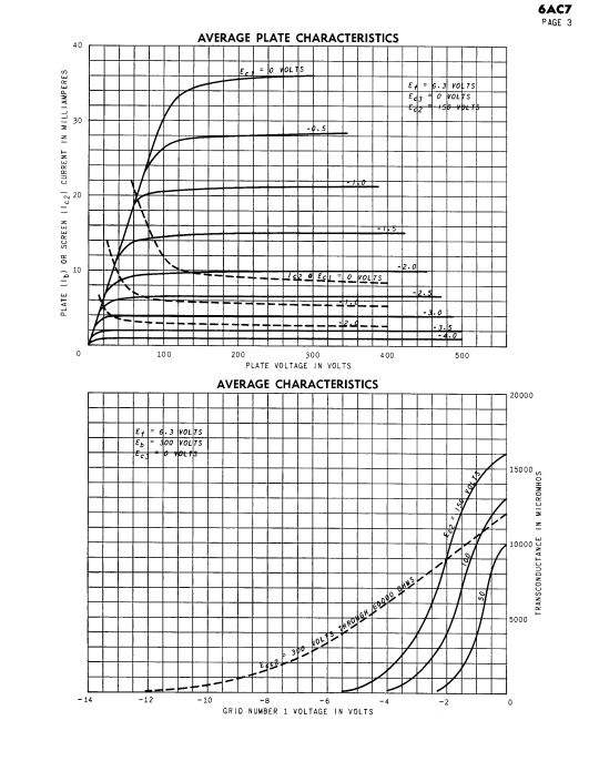

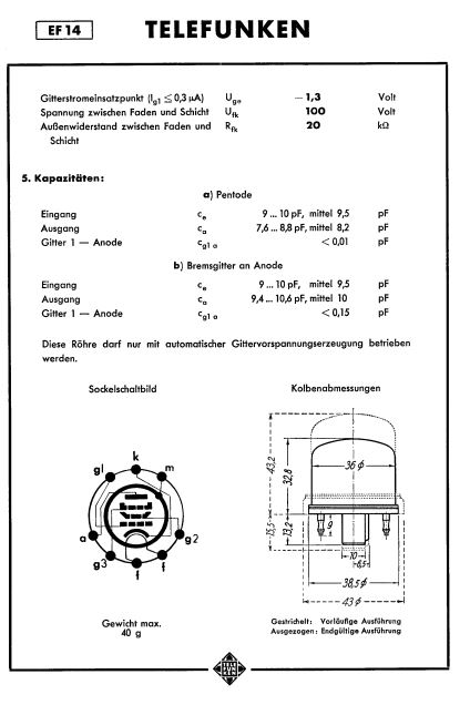
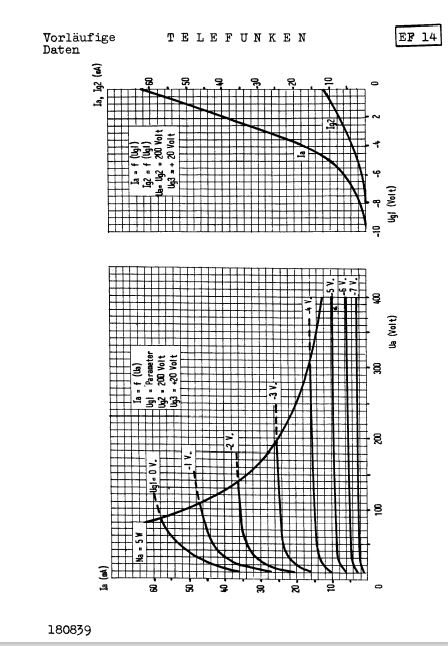
The EF50 was used in a great number of pulse and timing circuits as well
as an IF and RF amplifier.
Many of these circuits involved suppressor control of the plate current.
Data on the EF50 is difficult to find, so full data is included here.